EP0224645A2 - Elektronischer Triggerschalter für Prüfabschlusseinheit - Google Patents
Elektronischer Triggerschalter für Prüfabschlusseinheit Download PDFInfo
- Publication number
- EP0224645A2 EP0224645A2 EP86110253A EP86110253A EP0224645A2 EP 0224645 A2 EP0224645 A2 EP 0224645A2 EP 86110253 A EP86110253 A EP 86110253A EP 86110253 A EP86110253 A EP 86110253A EP 0224645 A2 EP0224645 A2 EP 0224645A2
- Authority
- EP
- European Patent Office
- Prior art keywords
- trigger switch
- triac
- bidirectional
- switch
- termination unit
- Prior art date
- Legal status (The legal status is an assumption and is not a legal conclusion. Google has not performed a legal analysis and makes no representation as to the accuracy of the status listed.)
- Granted
Links
- 238000012423 maintenance Methods 0.000 title claims abstract description 18
- 230000002457 bidirectional effect Effects 0.000 claims abstract description 26
- 239000004065 semiconductor Substances 0.000 claims abstract description 17
- XUIMIQQOPSSXEZ-UHFFFAOYSA-N Silicon Chemical compound [Si] XUIMIQQOPSSXEZ-UHFFFAOYSA-N 0.000 claims abstract description 13
- 229910052710 silicon Inorganic materials 0.000 claims abstract description 13
- 239000010703 silicon Substances 0.000 claims abstract description 13
- 230000004044 response Effects 0.000 description 10
- 238000010586 diagram Methods 0.000 description 9
- 238000012360 testing method Methods 0.000 description 6
- 230000002146 bilateral effect Effects 0.000 description 5
- 230000004048 modification Effects 0.000 description 3
- 238000012986 modification Methods 0.000 description 3
- 238000004519 manufacturing process Methods 0.000 description 2
- 239000003990 capacitor Substances 0.000 description 1
- 230000003247 decreasing effect Effects 0.000 description 1
- 238000009434 installation Methods 0.000 description 1
- 230000007257 malfunction Effects 0.000 description 1
- 230000009467 reduction Effects 0.000 description 1
- 230000001960 triggered effect Effects 0.000 description 1
Images

Classifications
-
- H—ELECTRICITY
- H04—ELECTRIC COMMUNICATION TECHNIQUE
- H04M—TELEPHONIC COMMUNICATION
- H04M3/00—Automatic or semi-automatic exchanges
- H04M3/22—Arrangements for supervision, monitoring or testing
- H04M3/26—Arrangements for supervision, monitoring or testing with means for applying test signals or for measuring
- H04M3/28—Automatic routine testing ; Fault testing; Installation testing; Test methods, test equipment or test arrangements therefor
- H04M3/30—Automatic routine testing ; Fault testing; Installation testing; Test methods, test equipment or test arrangements therefor for subscriber's lines, for the local loop
- H04M3/301—Circuit arrangements at the subscriber's side of the line
-
- H—ELECTRICITY
- H03—ELECTRONIC CIRCUITRY
- H03K—PULSE TECHNIQUE
- H03K17/00—Electronic switching or gating, i.e. not by contact-making and –breaking
- H03K17/30—Modifications for providing a predetermined threshold before switching
- H03K17/305—Modifications for providing a predetermined threshold before switching in thyristor switches
Definitions
- This invention relates to electronic devices used to trigger thyristors, and in particular to electronic trigger switches used in telephone maintenance termination units.
- the thyristor family of semiconductor devices consists of several very useful devices, including silicon controlled rectifiers (SCRs), DIACS, and TRIACS. Thyristors are characterized by having two states, an on-state and an off-state, making them useful for electric power regulation, switching, and phase control.
- SCRs silicon controlled rectifiers
- DIACS DIACS
- TRIACS TRIACS
- An SCR is a unidirectional PNPN semiconductor device having an anode, a cathode, and a gate. In the off-state, an SCR is a high-resistance, low- current circuit element at voltages up to its breakover voltage. A momentary positive pulse applied to the gate of an SCR will bias the device so that it switches to the on-state and becomes a low- resistance, high-current element. Once an SCR is in the on-state, it will remain in the on-state until the principal anode to cathode current drops below the holding current of the device.
- a TRIAC is a bidirectional thyristor which functions to control power in an AC electric circuit.
- the operation of a TRIAC can be related to two SCRs connected in inverse parallel.
- a TRIAC has a single gate, and the device can be triggered to the on-state by a gate pulse of either polarity.
- a TRIAC operates in a circuit in both directions essentially the same as an SCR behaves in its forward direction.
- a DIAC is essentially an open base NPN transistor.
- a DIAC is essentially an open base NPN transistor.
- a DIAC is a bidirectional circuit element which exhibits a high impedance state at voltages up to its voltage breakover point. Above the voltage breakover point a DIAC enters its on-state region, where current flows through the device as it exhibits decreasing resisitivity. Because of these characteristics, a DIAC can be used in a resistor-capacitor AC circuit to produce a bidirectional pulsing oscillator.
- a DIAC is an economical bidirectional device for triggering TRIACs in phase control circuits.
- a power control circuit having a low voltage, low current triggering response with a relatively high holding current requirement.
- the high holding current can be provided by a TRIAC, but a standard DIAC does not provide the desired triggering characteristics for a TRIAC in such an application. This is because a standard DIAC has a higher voltage requirement and does not switch on completely at the breakover point.
- To achieve low voltage triggering capability for TRIACs it has been necessary to construct relatively complicated triggering circuits comprising a plurality of transistors, resistors, and diodes. in a bridge network. Such circuits have been simplified only to a limited extent by placing two integrated circuits on a chip to produce a silicon bilateral switch (SBS) such as the General Electric type 2N4991.
- SBS silicon bilateral switch
- a specific application which requires a low voltage trigger switch for a TRIAC is the maintenance termination unit (MTU) of a telephone line.
- the MTU is a diagnostic circuit placed at the subscriber's terminal of a telephone line and used for analyzing faults and maintaining the line.
- An MTU provided by the Western Electric Company utilizes a complicated trigger circuit to provide the specific low voltage switching capability necessary for the desired MTU response characteristics.
- An additional line testing device is described in U.S. Patent No. 4,169,220 issued to Gary Fields on September 25, 1979 and entitled "Telephone Instrument Connection block with Remotely Actuated Line Test". Because of the very large number of MTUs required to update telephone systems around the country, it is highly desirable to provide a simple, economical trigger switch to replace the complicated circuitry now used as a bidirectional, low voltage switch for the TRIAC in the MTU.
- the present invention comprises a telephone maintenance termination unit (MTU) having a low voltage, bidirectional trigger switch as a component.
- An MTU is a diagnostic circuit which is permanently installed at the subscriber's terminal of a telephone line.
- An MTU is utilized by the telephone company to analyze faults and perform maintenance on the line.
- the MTU currently provided by the Western Electric Company utilizes a complicated trigger circuit containing a multiplicity of elements to provide the specific low voltage switching performance necessary for the proper MTU response characteristics.
- the MTU of the present invention contains a trigger switch which replaces the complex trigger circuitry of existing devices with a much simpler and more economical device.
- a major element of the previously existing MTU devices is a TRIAC, which must be switched to the on-state by a trigger circuit or device which functions at a very low current level and within a narrow, specific low voltage range.
- the MTU of the present invention utilizes a bidirectional trigger switch of several different embodiments, all of which are simpler, less costly, and easier to fabricate and install than the currently used trigger circuits.
- One embodiment of the invention comprises two sensitive silicon c ⁇ >ntrnlled rectifiers (SCRs) connected in inverse parallel relationship, such that the anode of one is connected to the cathode of the other and the gates are connected directly to each other.
- SCRs sensitive silicon c ⁇ >ntrnlled rectifiers
- the electronic trigger switch of the MTU is a silicon trigger switch (STS).
- STS is a diffused semiconductor device having an anode at one end, a cathode at the other end, and an electrical behavior similar to two sensitive SCRs connected in inverse parallel relationship.
- the bidirectional electronic trigger switch is replaced by a DIAC having specialized, low voltage breakover characteristics.
- the electronic trigger switch comprises a silicon bilateral switch (SBS) similar to the General Electric type 2N4991, but having specialized, low voltage breakover characteristics.
- One such embodiment replaces the TRIAC and trigger circuitry of the MTU with two non-sensitive SCRs connected in inverse parallel with their gate terminals joined using an STS such as described above.
- Another embodiment of the invention combines the TRIAC of the MTU and its associated trigger circuitry into one integrated circuit chip- called a SIDAC.
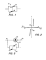
- Trigger switch 10 comprises sensitive silicon controlled rectifier (SCR) 12 and sensitive SCR 16.
- Sensitive SCRs such as the EC]03 series of SCRs manufactured by Teccor Electronics, Inc., have very high gate impedence but require very low gate current, on the order of 12 to 500 microamperes, to trigger the SCRs to the conductive on-state.
- Trigger switch 10 is constructed by connecting the anode of SCR 12 to the cathode of SCR 16 and the anode of SCR 16 to the cathode of SCR 12. To complete the connection, the gate electrode 14 of SCR 12 is connected directly to the gate electrode 18 of SCR 16. The resulting circuit produces trigger switch 10, which is a two-terminal, bidirectional device.
- the voltage-current response curve of trigger switch 10 is illustrated in FIGURE 2.
- the connection of identical SCRs in the inverse parallel configuration of FIGURE 1 produces the symmetrical, bilateral response curve shown in FIGURE 2.
- PAV peak inverse voltage
- the current flowing out of the gate of the reverse-biased SCR enters the gate of the forward-biased SCR and switches the forward-biased SCR to the on-state, allowing principal current to flow through the forward-biased SCR and thus through trigger switch 10.
- the voltage-current curve of FIGURE 2 shows the bidirectional behavior of trigger switch 10 by illustrating the symmetrical response as trigger switch 10 is biased in opposite directions. It can be seen that the Peak Inverse Voltage (PIV) of the reverse-biased SCR gate to cathode, corresponds to the breakover voltage 22, 24 of the trigger switch 10. Once the forward-biased SCR is switched to the on-state, the trigger switch 10 will remain in the conductive state as long as the principal current exceeds the minimum holding current 26, 28 of the forward-biased SCR.
- PV Peak Inverse Voltage
- Trigger switch 10 is shown connected to the gate 31 of TRIAC 30 to act as a trigger for TRIAC 30.
- a TRIAC such as logic TRIAC L201E7 manufactured by . Teccor Electronics, Inc., is a power control device which requires a gate trigger current of about 3 to 25 milliamperes of either polarity to switch the TRIAC to the on-state.
- the use of trigger switch 10 in conjunction with TRIAC 30, as shown in FIGURE 3 produces a circuit, having terminals 32 and 33, that has the characteristics of a low switching current, a high holding current, and a specific low voltage breakover point of either polarity.
- a specific embodiment of the present invention is the telephone maintenance termination unit (MTU) 40 illustrated schematically in FIGURE 4.
- MTU 40 has terminals 41 and 42, which connect to the telephone line coming from the telephone company's central oftice, and terminals 43 and 44, which connect to the subscriber's telephone set.
- the line connected to terminal 41 is referred to as the "tip", and the line connected to terminal 42 is referred to as the "ring”.
- the telephone company uses the MTU as a diagnostic circuit to test for faults or malfunctions in the telephone line servicing the subscriber.
- the telephone company applies electrical test signals to terminals 41 and 42 and receives a response depending upon the voltage of the test signal, the state of the MTU, and the presence of faults in the line or in the subscriber's telephone.
- the MTU provided by the Western Electric Company utilizes a TRIAC similar to TRIAC 30 and a'trigger circuit comprising at least two transistors, two resistors, and a rectifier bridge.
- the complicated circuitry provided by Western Electric is designed to trigger the TRIAC in the MTU with a low current and a low voltage in the narrow range of about 16 to 19 volts.
- the present invention provides MTU 40 with TRIAC 30 and electronic trigger switch 10 as shown in FIGURE 3 and described above.
- the circuit of FIGURE 3 which utilizes trigger switch 10 having two SCRs connected in inverse parallel relationship, is connected to both the "tip" line and the "ring" line of MTU 40 at nodes 32 and 33.
- the simplified circuitry of the present invention connected between nodes 32 and 33 as shown in FIGURE 4, replaces the complicated circuitry provided by the Western Electric Company.
- the MTU of the present invention is designed to provide the same test signal response as the Western Electric MTU. However, the MTU of the present invention uses fewer circuit elements and a simpler circuit, thus providing cost savings associated with fewer components and easier circuit fabrication. The potential savings is large due to the very large number of MTUs which are to be installed on telephone lines around the world.
- FIGURES 5-8 illustrate alternative circuits that may be connected between nodes 32 and 33 of MTU 40.
- FIGURE 5 shows a silicon trigger switch (STS) 55 that replaces the electronic trigger switch 10 in the circuit of FIGURE 3.
- STS 55 is a two-terminal, bidirectional, diffused PNPN semiconductor device which functions with a voltage-current response similar to that of trigger switch 10.
- STS 55 is a simplification of MTU 40, wherein the two inverse parallel SCRs of trigger switch 10 are combined and fabricated in a single semiconductor chip having two terminals.
- FIGURE 6 illustrates another embodiment of MTU 40, wherein trigger switch 10 is replaced by a DIAC 66.
- DIAC 66 is designed specifically to have an abrupt, bilateral, low voltage breakover point so as to trigger TRIAC 30 in the same manner as trigger switch 10 or STS 55. This design further simplifies the circuit shown in FIGURE 5 by replacing STS 55 with DIAC 66, which is a less complex semiconductor device.
- FIGURE 7 An embodiment of the present invention which simplifies the circuit of MTU 40 even further is shown in FIGURE 7.
- Tne TRIAC 30 and the trigger switch 10, connected between nodes 32 and 33 of MTU 40, are replaced by a single, two-terminal semiconductor device referred to as a SIDAC 77.
- SIDAC 77 has the same low voltage, low current triggering characteristics, and high holding current characteristics, as the circuits described in conjunction with FIGURES 3, 5, and 6 above.
- SIDAC 77 is a more complicated semiconductor device than TRIAC 30, STS 55, or DIAC 66, but it is designed to provide fabrication and installation cost savings by combining several circuit elements into a single two-terminal device that functions effectively in a telephone system MTU.
- FIGURE 8 illustrates an alternative embodiment of the present invention wherein the circuit between nodes 32 and 33 of MTU 40 comprises non-sensitive SCRs 81 and 83 connected in inverse parallel relationship.
- SCRs 81 and 83 take the place of TRIAC 30 in MTU 40.
- Gates 82 and 84 of SCRs 81 and 83 are connected to opposite terminals of an STS 55, as shown in FIGURE 8.
- Non-sensitive SCRs 81 and 83 provide the same power handling and high holding current characteristics of TRIAC 30 which they replace, and STS 55 provides low voltage, low current triggering for SCRs 81 and 83.
- the trigger switch 10 of MTU 40 is replaced by a silicon bilateral switch (SBS) similar to the SBS type 2N4991 manufactured by the General Electric Company.
- SBS silicon bilateral switch
- the use of SBS 2N4991 provides only a slight simplification over the Western Electric MTU circuit.
- the SBS type 2N4991 is essentially two integrated circuits joined on a single semiconductor chip.
- present SBS circuits would require modification to produce the response characteristics that would enable them to function as trigger switches within an MTU.
Landscapes
- Engineering & Computer Science (AREA)
- Signal Processing (AREA)
- Devices For Supply Of Signal Current (AREA)
Applications Claiming Priority (2)
| Application Number | Priority Date | Filing Date | Title |
|---|---|---|---|
| US06/801,758 US4685120A (en) | 1985-11-26 | 1985-11-26 | Electronic trigger switch for maintenance termination unit |
| US801758 | 1985-11-26 |
Publications (3)
| Publication Number | Publication Date |
|---|---|
| EP0224645A2 true EP0224645A2 (de) | 1987-06-10 |
| EP0224645A3 EP0224645A3 (en) | 1988-05-18 |
| EP0224645B1 EP0224645B1 (de) | 1993-03-17 |
Family
ID=25181978
Family Applications (1)
| Application Number | Title | Priority Date | Filing Date |
|---|---|---|---|
| EP86110253A Expired - Lifetime EP0224645B1 (de) | 1985-11-26 | 1986-07-25 | Elektronischer Triggerschalter für Prüfabschlusseinheit |
Country Status (3)
| Country | Link |
|---|---|
| US (1) | US4685120A (de) |
| EP (1) | EP0224645B1 (de) |
| DE (1) | DE3688044T2 (de) |
Cited By (2)
| Publication number | Priority date | Publication date | Assignee | Title |
|---|---|---|---|---|
| GB2221124A (en) * | 1988-07-22 | 1990-01-24 | Teradyne Inc | Testing telephone systems using anti parallel rectifying switches |
| EP0564063A1 (de) * | 1992-01-08 | 1993-10-06 | Gpt Limited | Abschlusseinheit mit Wartungsanordnung |
Families Citing this family (5)
| Publication number | Priority date | Publication date | Assignee | Title |
|---|---|---|---|---|
| US5111058A (en) * | 1990-05-23 | 1992-05-05 | Martin Richard A | Circuit for sustaining power supply output following momentary interruption of commercial a.c. power |
| US5357556A (en) * | 1992-08-10 | 1994-10-18 | Pacific Bell | System and method for telephone network testing |
| US6781161B1 (en) | 2003-04-09 | 2004-08-24 | Teccor Electronics, Lp | Non-gated thyristor device |
| CA2641698C (en) | 2006-02-10 | 2011-06-21 | Danfoss A/S | Control of a system with a large thermal capacity |
| TW201110821A (en) * | 2009-09-04 | 2011-03-16 | Fitipower Integrated Tech Inc | Drive apparatus and lighting apparatus |
Family Cites Families (6)
| Publication number | Priority date | Publication date | Assignee | Title |
|---|---|---|---|---|
| FR1430418A (fr) * | 1964-02-07 | 1966-03-04 | Thomson Houston Comp Francaise | Circuits de commande pourvus de semiconducteurs bidirectionnels |
| US4169220A (en) * | 1978-10-02 | 1979-09-25 | Fields Gary C | Telephone instrument connection block with remotely actuated line test |
| US4415779A (en) * | 1981-06-15 | 1983-11-15 | Western Electric Company, Inc. | Methods of and apparatus for testing telephone subscriber loop to locate a fault relative to a reference point |
| US4373121A (en) * | 1981-06-15 | 1983-02-08 | Bell Telephone Laboratories, Incorporated | Maintenance termination device |
| US4396809A (en) * | 1981-08-03 | 1983-08-02 | Bell Telephone Laboratories, Incorporated | Maintenance termination unit |
| US4529847A (en) * | 1983-12-12 | 1985-07-16 | At&T Bell Laboratories | Maintenance termination unit |
-
1985
- 1985-11-26 US US06/801,758 patent/US4685120A/en not_active Expired - Lifetime
-
1986
- 1986-07-25 EP EP86110253A patent/EP0224645B1/de not_active Expired - Lifetime
- 1986-07-25 DE DE8686110253T patent/DE3688044T2/de not_active Expired - Fee Related
Cited By (5)
| Publication number | Priority date | Publication date | Assignee | Title |
|---|---|---|---|---|
| GB2221124A (en) * | 1988-07-22 | 1990-01-24 | Teradyne Inc | Testing telephone systems using anti parallel rectifying switches |
| GB2256332A (en) * | 1988-07-22 | 1992-12-02 | Teradyne Inc | Antiparallel rectifying switches for testing telephone systems. |
| GB2256332B (en) * | 1988-07-22 | 1993-02-17 | Teradyne Inc | Testing telephone systems |
| GB2221124B (en) * | 1988-07-22 | 1993-02-24 | Teradyne Inc | Testing telephone systems |
| EP0564063A1 (de) * | 1992-01-08 | 1993-10-06 | Gpt Limited | Abschlusseinheit mit Wartungsanordnung |
Also Published As
| Publication number | Publication date |
|---|---|
| DE3688044T2 (de) | 1993-06-24 |
| EP0224645A3 (en) | 1988-05-18 |
| DE3688044D1 (de) | 1993-04-22 |
| EP0224645B1 (de) | 1993-03-17 |
| US4685120A (en) | 1987-08-04 |
Similar Documents
| Publication | Publication Date | Title |
|---|---|---|
| JPH061941B2 (ja) | 電話加入者ル−プ過電圧保護回路 | |
| HK8095A (en) | Control circuit for a bistable relay | |
| US4685120A (en) | Electronic trigger switch for maintenance termination unit | |
| US4827497A (en) | Electronic trigger switch for maintenance termination unit | |
| KR880700602A (ko) | 전화 라인 스위치 | |
| GB1574078A (en) | Voltage-limiting circuit | |
| WO1991008617A1 (en) | Symmetrical controlled switching circuit | |
| GB1377242A (en) | End mark controlled switching system and matrix | |
| JPH0850518A (ja) | 過電流保護装置 | |
| GB2104286A (en) | Controlled-breakover bidirectional semiconductor switch | |
| US11171645B1 (en) | Transistor switching circuit and integrated circuit thereof | |
| RU2020742C1 (ru) | Тиристорный коммутатор | |
| EP0224644B1 (de) | Elektronischer Triggerschalter | |
| US4626632A (en) | Maintenance termination unit | |
| US4614962A (en) | Controlled electronic switching device for the suppression of transients | |
| US4049976A (en) | Solid-state voltage switching circuit | |
| JPS60117855A (ja) | 加入者ループ開放装置 | |
| EP0085089B1 (de) | Einrichtung zum linearisieren von halbleiterkreuzpunkten | |
| US3346744A (en) | Power control circuits | |
| US5418834A (en) | Maintenance termination units | |
| EP0182393A2 (de) | Ausschlusseinrichtung für parallel geschaltete Fernsprecher | |
| US3956590A (en) | Switching arrangement for switching between different current values by means of mechanical or electronic switches | |
| WO1995023455A1 (en) | Switching device for telecommunications channel | |
| US3389228A (en) | Controlled latching semiconductor switch and switching network | |
| Hartman et al. | 530V Integrated gated diode switch for telecommunications |
Legal Events
| Date | Code | Title | Description |
|---|---|---|---|
| PUAI | Public reference made under article 153(3) epc to a published international application that has entered the european phase |
Free format text: ORIGINAL CODE: 0009012 |
|
| AK | Designated contracting states |
Kind code of ref document: A2 Designated state(s): BE CH DE FR GB IT LI SE |
|
| PUAL | Search report despatched |
Free format text: ORIGINAL CODE: 0009013 |
|
| AK | Designated contracting states |
Kind code of ref document: A3 Designated state(s): BE CH DE FR GB IT LI SE |
|
| 17P | Request for examination filed |
Effective date: 19881028 |
|
| 17Q | First examination report despatched |
Effective date: 19901115 |
|
| GRAA | (expected) grant |
Free format text: ORIGINAL CODE: 0009210 |
|
| ITF | It: translation for a ep patent filed | ||
| AK | Designated contracting states |
Kind code of ref document: B1 Designated state(s): BE CH DE FR GB IT LI SE |
|
| REF | Corresponds to: |
Ref document number: 3688044 Country of ref document: DE Date of ref document: 19930422 |
|
| ET | Fr: translation filed | ||
| PLBE | No opposition filed within time limit |
Free format text: ORIGINAL CODE: 0009261 |
|
| STAA | Information on the status of an ep patent application or granted ep patent |
Free format text: STATUS: NO OPPOSITION FILED WITHIN TIME LIMIT |
|
| 26N | No opposition filed | ||
| EAL | Se: european patent in force in sweden |
Ref document number: 86110253.1 |
|
| PGFP | Annual fee paid to national office [announced via postgrant information from national office to epo] |
Ref country code: SE Payment date: 20000705 Year of fee payment: 15 |
|
| PGFP | Annual fee paid to national office [announced via postgrant information from national office to epo] |
Ref country code: FR Payment date: 20000711 Year of fee payment: 15 |
|
| PGFP | Annual fee paid to national office [announced via postgrant information from national office to epo] |
Ref country code: GB Payment date: 20000719 Year of fee payment: 15 |
|
| PGFP | Annual fee paid to national office [announced via postgrant information from national office to epo] |
Ref country code: DE Payment date: 20000724 Year of fee payment: 15 |
|
| PGFP | Annual fee paid to national office [announced via postgrant information from national office to epo] |
Ref country code: CH Payment date: 20000726 Year of fee payment: 15 |
|
| PGFP | Annual fee paid to national office [announced via postgrant information from national office to epo] |
Ref country code: BE Payment date: 20000918 Year of fee payment: 15 |
|
| PG25 | Lapsed in a contracting state [announced via postgrant information from national office to epo] |
Ref country code: GB Free format text: LAPSE BECAUSE OF NON-PAYMENT OF DUE FEES Effective date: 20010725 |
|
| PG25 | Lapsed in a contracting state [announced via postgrant information from national office to epo] |
Ref country code: SE Free format text: LAPSE BECAUSE OF NON-PAYMENT OF DUE FEES Effective date: 20010726 |
|
| PG25 | Lapsed in a contracting state [announced via postgrant information from national office to epo] |
Ref country code: LI Free format text: LAPSE BECAUSE OF NON-PAYMENT OF DUE FEES Effective date: 20010731 Ref country code: CH Free format text: LAPSE BECAUSE OF NON-PAYMENT OF DUE FEES Effective date: 20010731 Ref country code: BE Free format text: LAPSE BECAUSE OF NON-PAYMENT OF DUE FEES Effective date: 20010731 |
|
| BERE | Be: lapsed |
Owner name: TECCOR ELECTRONICS INC. Effective date: 20010731 |
|
| EUG | Se: european patent has lapsed |
Ref document number: 86110253.1 |
|
| REG | Reference to a national code |
Ref country code: CH Ref legal event code: PL |
|
| GBPC | Gb: european patent ceased through non-payment of renewal fee |
Effective date: 20010725 |
|
| PG25 | Lapsed in a contracting state [announced via postgrant information from national office to epo] |
Ref country code: FR Free format text: LAPSE BECAUSE OF NON-PAYMENT OF DUE FEES Effective date: 20020329 |
|
| PG25 | Lapsed in a contracting state [announced via postgrant information from national office to epo] |
Ref country code: DE Free format text: LAPSE BECAUSE OF NON-PAYMENT OF DUE FEES Effective date: 20020501 |
|
| REG | Reference to a national code |
Ref country code: FR Ref legal event code: ST |
|
| PG25 | Lapsed in a contracting state [announced via postgrant information from national office to epo] |
Ref country code: IT Free format text: LAPSE BECAUSE OF NON-PAYMENT OF DUE FEES Effective date: 20050725 |