EP0218241A2 - Filtre en peigne à deux dimensions - Google Patents
Filtre en peigne à deux dimensions Download PDFInfo
- Publication number
- EP0218241A2 EP0218241A2 EP86113923A EP86113923A EP0218241A2 EP 0218241 A2 EP0218241 A2 EP 0218241A2 EP 86113923 A EP86113923 A EP 86113923A EP 86113923 A EP86113923 A EP 86113923A EP 0218241 A2 EP0218241 A2 EP 0218241A2
- Authority
- EP
- European Patent Office
- Prior art keywords
- comb filter
- summing junction
- input
- delay
- color television
- Prior art date
- Legal status (The legal status is an assumption and is not a legal conclusion. Google has not performed a legal analysis and makes no representation as to the accuracy of the status listed.)
- Withdrawn
Links
Images


Classifications
-
- H—ELECTRICITY
- H04—ELECTRIC COMMUNICATION TECHNIQUE
- H04N—PICTORIAL COMMUNICATION, e.g. TELEVISION
- H04N9/00—Details of colour television systems
- H04N9/77—Circuits for processing the brightness signal and the chrominance signal relative to each other, e.g. adjusting the phase of the brightness signal relative to the colour signal, correcting differential gain or differential phase
- H04N9/78—Circuits for processing the brightness signal and the chrominance signal relative to each other, e.g. adjusting the phase of the brightness signal relative to the colour signal, correcting differential gain or differential phase for separating the brightness signal or the chrominance signal from the colour television signal, e.g. using comb filter
-
- H—ELECTRICITY
- H03—ELECTRONIC CIRCUITRY
- H03H—IMPEDANCE NETWORKS, e.g. RESONANT CIRCUITS; RESONATORS
- H03H17/00—Networks using digital techniques
- H03H17/02—Frequency selective networks
- H03H17/0202—Two or more dimensional filters; Filters for complex signals
-
- H—ELECTRICITY
- H03—ELECTRONIC CIRCUITRY
- H03H—IMPEDANCE NETWORKS, e.g. RESONANT CIRCUITS; RESONATORS
- H03H17/00—Networks using digital techniques
- H03H17/02—Frequency selective networks
- H03H17/0202—Two or more dimensional filters; Filters for complex signals
- H03H2017/0204—Comb filters
Definitions
- the present invention relates to processing apparatus for processing signals characterized by multiple time base. More particularly, the present invention relates to linear multi-dimensional processing of multiple time base signals such as quadrature modulated color television signals.
- the first class suffers from loss of luminance diagonal resolution, loss of chroma vertical resolution, and cross-color and cross-luminance patterns in certain picture conditions.
- the second class suffers from chroma blurring with motion, positional errors in luminance high frequencies during picture motion, and occurrence of certain cross-color and cross-luminance patterns with certain motion speeds in the picture image.
- the signal follows the NTSC format and the first period corresponds to one of a picture frame and a picture scanning line, and the second period corresponds to the other thereof, or the signal follows the PAL format and the first period corresponds to one of two picture frames and two picture scanning lines and the second period corresponds to the other thereof.
- the improved multi-dimensional comb filter system is specifically applied to separation of chrominance and luminance information in a quadrature modulated color television signal and includes an input for receiving the quadrature modulated color television signal; a first comb filter connected to the input and operating at a period related to one of picture frame and picture line, for separating a predetermined one of chrominance and luminance from the color television signal; a second comb filter connected to the first comb filter and operating at the period related to the other of picture frame and picture line, for further separating the predetermined one of chrominance and luminance; a delay matching network connected to the input for delay the color television signal corresponding to the predetermined one of chrominance and luminance put out by the second comb filter by providing a delay corresponding to picture frame and picture line periods; and a linear adder circuit connected to the second comb filter and to the delay matching network for combining in phase the delayed color television signal and the predetermined one of chrominance and luminance put out by the second comb
- the first comb filter operates at the period of a picture frame and comprises a portion of the delay matching network by delaying the color television signal by a picture frame delay portion of the overall picture frame and line period delay required.
- a specific object of the present invention is to provide an improved, linearly operating bidimensional comb filter system for separating luminance and chrominance components of a quadrature modulated color television signal without switching or adaptivity to picture conditions and without introduction of unwanted picture artifacts.
- Another object of the present invention is to provide a simple, bidimensional comb filter system for color television signal component processing which overcomes limitations and drawbacks of the prior art at low cost, and thereby lends itself to inclusion in mass produced consumer oriented television signal reception and display apparatus.
- One further object of the present invention is to achieve a multi-dimensional comb filter system which advantageously utilizes low cost semiconductor digital conversion and storage elements.
- the signal at the input 12 enters an "M domain" comb filter 14.
- the M domain corresponds to the period of a television picture frame, and at least one frame store is used in order to achieve a picture frame domain comb filter.
- the M domain comb filter 14 is preferably implemented with digital techniques as are well known and available to those skilled in the art.
- the output of the N domain comb filter 16 enters one input of a linear adder circuit 18.
- Another input to the linear adder circuit 18 comes from a matching delay matrix 20 which delays the original signal precisely by the periods corresponding to M and N (frame and line periods in the preferred application).
- M corresponds to one frame period
- N corresponds to one line period
- M corresponds to two frame periods
- N corresponds to two line periods.
- An output 22 of the system 10 provides separated data of a type which has been selected and separated by the bidimensional comb filtering process, such as chrominance or luminance.
- a second branch from the node 106 passes through an amplifier 114 having a minus one half unity gain factor to the summing circuit 112.
- the reference numeral 116 points to the minus sign of the gain factor for the amplifier 114 to denote that it acts as an inverter in the instance of luminance separation. Should the system 100 be intended for the separation of chrominance, the minus sign 116 would be changed to a plus sign, and the amplifier 116 would operate with a plus one half unity gain factor.
- An amplifier 118 having a one quarter unity gain factor has an input connected to the input 102 and an output connected to the summing circuit 112.
- the summing circuits 112 combines the three input values and puts out the sum thereof at an output node 120.
- a second comb filter 122 operates at the picture line rate (1/15,750 second).
- the signal from the output node 120 passes through a one line delay 124 to reach a node 126 which provides a two way branch of the resultant, delayed signal.
- a first branch passes through a second one line delay 128 and a one quarter gain factor amplifier 130 to reach a second summing circuit 132.
- the signal at the output node 140 is passed through a unity gain inverter 142 and combined in a third summing circuit 144 with a one frame delayed signal from the third branch of the node 106 of the first comb filter 102 which has been further delayed by the period of one line by first passing through a line delay 146.
- delay matching is provided by the use of the first frame delay 104 and a third one line delay 146.
- the delays provided by the frame delays 104 and 108 correspond to two frame periods, and the delays provided by the line delays 124, 128 and 146 correspond to two line periods.
- the output D of the first comb filter 102 is other than zero for luminance.
- the signal D is equal to the signal E which is equal to the signal F.
- the output signal G at the node 140 is equal to the following expression:
- D -1
- the luminance transition becomes averaged over a few lines, with some slight blurring.
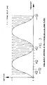
- the comb filtering action provided by the tandem arrangement of frame and line comb filters in the system 100 is depicted by the output waveform diagram of Fig. 3.
- the luminance components are maximally present at each even multiple of the line frequency n and are minimally present at the odd multiples thereof.
- the low frequency sine wave corresponds to the frame rate and shows how the frame rate is used to enhance the comb filtering action of the system 100.
- the ordering of the frame comb filter 102 and the line comb filter 122 in the tandem system 100 is immaterial, since there is no interactivity between the two filters.
- some practical cost savings are presently realized by placing the frame filter 102 before the line filter 122, so that the first delay 104 of the filter 102 may also provide the required one frame delay portion of the overall original signal delay (one frame and one line).
- This arrangement requires only one additional line delay 146 and results in a less expensive implementation than if an additional frame delay were required, as frame delays are presently more expensive than line delays.
- FIG. 4 A practical example of an improved color encoder 200 for a quadrature modulated color television picture signal system is depicted in overview in Fig. 4.
- a luminance signal at an input 202 is split into two paths, a first path through a 2.3 to 4 . 2 MH z band reject filter to an adder 206, and a second path through a 2 . 3 to 4 . 2 MHz band pass filter 20p and the luminance bidimensional comb filter 100 of Figs. 2 and a to the adder 206.
- Color components I and Q and color subcarrier on lines 212 , 2 1 4 and 216 respectively, enter a quadrature modulator 2 18 and pass through a chrominance bidimensional comb filter system 100 a (in which the signs 116 and 136 have been changed from minus to plus) to the adder 210.
- This encoder 200 puts out a color picture signal in which both luminance and chroma components have been enhanced by bidimensional comb filtering in accordance with the present invention before these components have been combined together.
- Fig. 5 illustrates an improved low cost decoder 300 for color television, suitable for inclusion in color television receiving apparatus intended for the consumer.
- the color television picture signal enters at an input 3 0 2 and passes through a chroma band pass and bidimensional comb filter 304.
- This filter 304 includes the elements 208 and 100a found in the Fig. 4 encoder.
- the separated chrominance component exiting the filter 304 is passed into a subtractor circuit 306 where it is subtracted from the color signal which has been suitably delayed by a delay matching circuit 308.
- the resultant difference is luminance which is put out on a luminance output line 310.
- the combed chroma component is then subjected to demodulation in a chroma demodulator 312 in order to recover the I and Q phase components making up the color s ignal.
- phase components together with luminance, are then passed through conventional color matrices 314 in order to recover the red (R), green (G) and blue (B) color components which are put out on lines 316, 318 and 320 respectively.
Landscapes
- Engineering & Computer Science (AREA)
- Physics & Mathematics (AREA)
- Computer Hardware Design (AREA)
- Mathematical Physics (AREA)
- Multimedia (AREA)
- Signal Processing (AREA)
- Processing Of Color Television Signals (AREA)
- Filters That Use Time-Delay Elements (AREA)
Applications Claiming Priority (2)
| Application Number | Priority Date | Filing Date | Title |
|---|---|---|---|
| US06/785,881 US4656459A (en) | 1985-10-07 | 1985-10-07 | Dual slope converter with large apparent integrator swing |
| US785881 | 1985-10-09 |
Publications (2)
| Publication Number | Publication Date |
|---|---|
| EP0218241A2 true EP0218241A2 (fr) | 1987-04-15 |
| EP0218241A3 EP0218241A3 (fr) | 1988-11-23 |
Family
ID=25136923
Family Applications (1)
| Application Number | Title | Priority Date | Filing Date |
|---|---|---|---|
| EP86113923A Withdrawn EP0218241A3 (fr) | 1985-10-07 | 1986-10-08 | Filtre en peigne à deux dimensions |
Country Status (2)
| Country | Link |
|---|---|
| EP (1) | EP0218241A3 (fr) |
| JP (1) | JPS62175092A (fr) |
Cited By (5)
| Publication number | Priority date | Publication date | Assignee | Title |
|---|---|---|---|---|
| EP0321312A1 (fr) * | 1987-12-18 | 1989-06-21 | Victor Company Of Japan, Limited | Circuit de suppression de composantes de diaphonie dans une signal à porteuse couleur |
| EP0352867A2 (fr) * | 1988-07-29 | 1990-01-31 | Lsi Logic Corporation | Filtre numérique reconfigurable utilisant un système multiprocesseur |
| EP0379766A1 (fr) * | 1987-01-30 | 1990-08-01 | Yves Charles Faroudja | Traitement vidéo dans lequel les composantes de haute fréquence du signal de luminance sont repliées dans un spectre de bande moyenne |
| EP0449656A2 (fr) * | 1990-03-30 | 1991-10-02 | Yves Charles Faroudja | Système de réduction du bruit de télévision dans le domaine temporel |
| US5260775A (en) * | 1990-03-30 | 1993-11-09 | Farouda Yves C | Time domain television noise reduction system |
Families Citing this family (2)
| Publication number | Priority date | Publication date | Assignee | Title |
|---|---|---|---|---|
| JPH0750847A (ja) * | 1990-04-27 | 1995-02-21 | Centre De Rech Ind Du Quebec | 複合ビデオ符号化/復号化用途のための分離可能ダイアモンド形状多次元フィルター |
| US5270803A (en) * | 1992-10-26 | 1993-12-14 | The Grass Valley Group, Inc. | Inverse hyperbolic comb filter |
Citations (1)
| Publication number | Priority date | Publication date | Assignee | Title |
|---|---|---|---|---|
| GB2138243A (en) * | 1983-04-12 | 1984-10-17 | Bosch Gmbh Robert | Arrangement for the separation of the luminance and colour information of a colour television signal |
-
1986
- 1986-10-08 EP EP86113923A patent/EP0218241A3/fr not_active Withdrawn
- 1986-10-09 JP JP24116486A patent/JPS62175092A/ja active Pending
Patent Citations (1)
| Publication number | Priority date | Publication date | Assignee | Title |
|---|---|---|---|---|
| GB2138243A (en) * | 1983-04-12 | 1984-10-17 | Bosch Gmbh Robert | Arrangement for the separation of the luminance and colour information of a colour television signal |
Non-Patent Citations (1)
| Title |
|---|
| IEEE TRANSACTIONS ON CONSUMER ELECTRONICS, vol. CE-31, no. 3, August 1985, pages 226-239, IEEE, New York, US; D. TEICHNER: "Quality improvement by adaptive inter-/intraframe processing in PAL TV receivers" * |
Cited By (9)
| Publication number | Priority date | Publication date | Assignee | Title |
|---|---|---|---|---|
| EP0379766A1 (fr) * | 1987-01-30 | 1990-08-01 | Yves Charles Faroudja | Traitement vidéo dans lequel les composantes de haute fréquence du signal de luminance sont repliées dans un spectre de bande moyenne |
| EP0321312A1 (fr) * | 1987-12-18 | 1989-06-21 | Victor Company Of Japan, Limited | Circuit de suppression de composantes de diaphonie dans une signal à porteuse couleur |
| US4930005A (en) * | 1987-12-18 | 1990-05-29 | Victor Company Of Japan, Ltd. | Circuit for removing crosstalk components in a carrier chrominance signal |
| US4969033A (en) * | 1987-12-18 | 1990-11-06 | Victor Company Of Japan, Ltd. | Circuit for removing crosstalk components in a carrier chrominance signal |
| EP0352867A2 (fr) * | 1988-07-29 | 1990-01-31 | Lsi Logic Corporation | Filtre numérique reconfigurable utilisant un système multiprocesseur |
| EP0352867A3 (fr) * | 1988-07-29 | 1991-05-29 | Lsi Logic Corporation | Filtre numérique reconfigurable utilisant un système multiprocesseur |
| EP0449656A2 (fr) * | 1990-03-30 | 1991-10-02 | Yves Charles Faroudja | Système de réduction du bruit de télévision dans le domaine temporel |
| EP0449656A3 (en) * | 1990-03-30 | 1992-03-18 | Yves Charles Faroudja | Time domain television noise reduction system |
| US5260775A (en) * | 1990-03-30 | 1993-11-09 | Farouda Yves C | Time domain television noise reduction system |
Also Published As
| Publication number | Publication date |
|---|---|
| EP0218241A3 (fr) | 1988-11-23 |
| JPS62175092A (ja) | 1987-07-31 |
Similar Documents
| Publication | Publication Date | Title |
|---|---|---|
| KR100388579B1 (ko) | 공통지연소자를갖는휘도/색차를분리시키기위한방법및장치 | |
| US4530004A (en) | Color television signal processing circuit | |
| US4551753A (en) | Picture signal processing system including spatio-temporal filter | |
| US4335395A (en) | Standards conversion of color television signals | |
| US4322739A (en) | Processing of N.T.S.C. color television signals | |
| CA1237517A (fr) | Emission de television en couleurs a adaptation de mouvement | |
| GB2186150A (en) | Bandwidth reduction and conversion of a progressive scan television signal using sum and difference components | |
| US4644389A (en) | Digital television signal processing circuit | |
| US4949166A (en) | Apparatus for combining and separating constituent components of a video signal | |
| US4786963A (en) | Adaptive Y/C separation apparatus for TV signals | |
| US4683490A (en) | Video signal processing apparatus | |
| US4460925A (en) | Method and apparatus for deriving a PAL color television signal corresponding to any desired field in an 8-field PAL sequence from one stored field or picture of a PAL signal | |
| EP0690632B1 (fr) | Décodeur numérique pour signaux vidéo et méthode de décodage numérique de signal vidéo | |
| EP0218241A2 (fr) | Filtre en peigne à deux dimensions | |
| US4333104A (en) | Color demodulating apparatus with cross-color cancellation | |
| EP0464879B1 (fr) | Système de séparation de signaux de luminance et de chrominance et méthode correspondante | |
| CA1245343A (fr) | Circuits de separation des signaux de luminance et de chrominance | |
| EP0364967B1 (fr) | Circuit de séparation des signaux luminance/chrominance pour un signal de télévision en couleurs PAL | |
| EP0329382B1 (fr) | Circuit pour la séparation des signaux de luminance et de chrominance | |
| CA1219343A (fr) | Dispositif pour reduire la distorsion produite par le mouvement dans un signal de chrominance obtenu par filtrage en peigne des cadres | |
| US4492976A (en) | Line standard conversion circuit for a television signal | |
| KR0158665B1 (ko) | 확장된 복합 텔레비젼 시스템 | |
| GB2044577A (en) | Method of and apparatus for coding and decoding PAL colour television signals | |
| EP0430049B1 (fr) | Circuit d'interpolation de signal de chrominance pour un signal de télévision couleur du type PAL | |
| JP2794156B2 (ja) | くし形フィルタ |
Legal Events
| Date | Code | Title | Description |
|---|---|---|---|
| PUAI | Public reference made under article 153(3) epc to a published international application that has entered the european phase |
Free format text: ORIGINAL CODE: 0009012 |
|
| AK | Designated contracting states |
Kind code of ref document: A2 Designated state(s): DE GB IT |
|
| PUAL | Search report despatched |
Free format text: ORIGINAL CODE: 0009013 |
|
| AK | Designated contracting states |
Kind code of ref document: A3 Designated state(s): DE GB IT |
|
| STAA | Information on the status of an ep patent application or granted ep patent |
Free format text: STATUS: THE APPLICATION IS DEEMED TO BE WITHDRAWN |
|
| 18D | Application deemed to be withdrawn |
Effective date: 19881101 |
|
| RIN1 | Information on inventor provided before grant (corrected) |
Inventor name: FAROUDJA, YVES C. |