EP0215847B1 - Procede et appareil de formation d'images numeriques - Google Patents
Procede et appareil de formation d'images numeriques Download PDFInfo
- Publication number
- EP0215847B1 EP0215847B1 EP19860901697 EP86901697A EP0215847B1 EP 0215847 B1 EP0215847 B1 EP 0215847B1 EP 19860901697 EP19860901697 EP 19860901697 EP 86901697 A EP86901697 A EP 86901697A EP 0215847 B1 EP0215847 B1 EP 0215847B1
- Authority
- EP
- European Patent Office
- Prior art keywords
- sensor
- image
- digital
- pixels
- elements
- Prior art date
- Legal status (The legal status is an assumption and is not a legal conclusion. Google has not performed a legal analysis and makes no representation as to the accuracy of the status listed.)
- Expired
Links
- 238000000034 method Methods 0.000 title claims description 16
- 230000003595 spectral effect Effects 0.000 claims abstract description 4
- 230000002950 deficient Effects 0.000 claims description 21
- 238000001429 visible spectrum Methods 0.000 claims 3
- 239000011521 glass Substances 0.000 description 12
- 238000005070 sampling Methods 0.000 description 6
- 230000008901 benefit Effects 0.000 description 4
- 230000000694 effects Effects 0.000 description 4
- 230000008520 organization Effects 0.000 description 4
- 239000011248 coating agent Substances 0.000 description 3
- 238000000576 coating method Methods 0.000 description 3
- 230000006870 function Effects 0.000 description 3
- 230000010354 integration Effects 0.000 description 3
- 230000003287 optical effect Effects 0.000 description 3
- 230000035945 sensitivity Effects 0.000 description 3
- PXHVJJICTQNCMI-UHFFFAOYSA-N Nickel Chemical compound [Ni] PXHVJJICTQNCMI-UHFFFAOYSA-N 0.000 description 2
- VYPSYNLAJGMNEJ-UHFFFAOYSA-N Silicium dioxide Chemical compound O=[Si]=O VYPSYNLAJGMNEJ-UHFFFAOYSA-N 0.000 description 2
- 238000006073 displacement reaction Methods 0.000 description 2
- 239000005304 optical glass Substances 0.000 description 2
- 230000008569 process Effects 0.000 description 2
- 239000000758 substrate Substances 0.000 description 2
- 230000001629 suppression Effects 0.000 description 2
- 239000003990 capacitor Substances 0.000 description 1
- 230000015556 catabolic process Effects 0.000 description 1
- 238000006243 chemical reaction Methods 0.000 description 1
- 238000010276 construction Methods 0.000 description 1
- 238000006731 degradation reaction Methods 0.000 description 1
- 238000010586 diagram Methods 0.000 description 1
- 230000002708 enhancing effect Effects 0.000 description 1
- 239000000835 fiber Substances 0.000 description 1
- 238000003384 imaging method Methods 0.000 description 1
- 229910001026 inconel Inorganic materials 0.000 description 1
- 239000011159 matrix material Substances 0.000 description 1
- 229910052759 nickel Inorganic materials 0.000 description 1
- 238000011084 recovery Methods 0.000 description 1
- 230000004044 response Effects 0.000 description 1
- 230000000717 retained effect Effects 0.000 description 1
- 238000000926 separation method Methods 0.000 description 1
- 235000012239 silicon dioxide Nutrition 0.000 description 1
- 239000000377 silicon dioxide Substances 0.000 description 1
- 238000002834 transmittance Methods 0.000 description 1
- WFKWXMTUELFFGS-UHFFFAOYSA-N tungsten Chemical compound [W] WFKWXMTUELFFGS-UHFFFAOYSA-N 0.000 description 1
- 229910052721 tungsten Inorganic materials 0.000 description 1
- 239000010937 tungsten Substances 0.000 description 1
Images


Classifications
-
- H—ELECTRICITY
- H04—ELECTRIC COMMUNICATION TECHNIQUE
- H04N—PICTORIAL COMMUNICATION, e.g. TELEVISION
- H04N1/00—Scanning, transmission or reproduction of documents or the like, e.g. facsimile transmission; Details thereof
- H04N1/04—Scanning arrangements, i.e. arrangements for the displacement of active reading or reproducing elements relative to the original or reproducing medium, or vice versa
- H04N1/19—Scanning arrangements, i.e. arrangements for the displacement of active reading or reproducing elements relative to the original or reproducing medium, or vice versa using multi-element arrays
- H04N1/195—Scanning arrangements, i.e. arrangements for the displacement of active reading or reproducing elements relative to the original or reproducing medium, or vice versa using multi-element arrays the array comprising a two-dimensional array or a combination of two-dimensional arrays
- H04N1/19505—Scanning picture elements spaced apart from one another in at least one direction
- H04N1/19515—Scanning picture elements spaced apart from one another in at least one direction in two directions
-
- H—ELECTRICITY
- H04—ELECTRIC COMMUNICATION TECHNIQUE
- H04N—PICTORIAL COMMUNICATION, e.g. TELEVISION
- H04N1/00—Scanning, transmission or reproduction of documents or the like, e.g. facsimile transmission; Details thereof
- H04N1/04—Scanning arrangements, i.e. arrangements for the displacement of active reading or reproducing elements relative to the original or reproducing medium, or vice versa
- H04N1/19—Scanning arrangements, i.e. arrangements for the displacement of active reading or reproducing elements relative to the original or reproducing medium, or vice versa using multi-element arrays
- H04N1/195—Scanning arrangements, i.e. arrangements for the displacement of active reading or reproducing elements relative to the original or reproducing medium, or vice versa using multi-element arrays the array comprising a two-dimensional array or a combination of two-dimensional arrays
- H04N1/19505—Scanning picture elements spaced apart from one another in at least one direction
- H04N1/19521—Arrangements for moving the elements of the array relative to the scanned image or vice versa
- H04N1/19526—Optical means
- H04N1/19536—Refracting elements
-
- H—ELECTRICITY
- H04—ELECTRIC COMMUNICATION TECHNIQUE
- H04N—PICTORIAL COMMUNICATION, e.g. TELEVISION
- H04N1/00—Scanning, transmission or reproduction of documents or the like, e.g. facsimile transmission; Details thereof
- H04N1/04—Scanning arrangements, i.e. arrangements for the displacement of active reading or reproducing elements relative to the original or reproducing medium, or vice versa
- H04N1/19—Scanning arrangements, i.e. arrangements for the displacement of active reading or reproducing elements relative to the original or reproducing medium, or vice versa using multi-element arrays
- H04N1/195—Scanning arrangements, i.e. arrangements for the displacement of active reading or reproducing elements relative to the original or reproducing medium, or vice versa using multi-element arrays the array comprising a two-dimensional array or a combination of two-dimensional arrays
- H04N1/19505—Scanning picture elements spaced apart from one another in at least one direction
- H04N1/19521—Arrangements for moving the elements of the array relative to the scanned image or vice versa
- H04N1/19526—Optical means
- H04N1/19552—Rotation of optical elements
- H04N1/19563—Rotation of optical elements about an axis perpendicular to the optical axis
-
- H—ELECTRICITY
- H04—ELECTRIC COMMUNICATION TECHNIQUE
- H04N—PICTORIAL COMMUNICATION, e.g. TELEVISION
- H04N1/00—Scanning, transmission or reproduction of documents or the like, e.g. facsimile transmission; Details thereof
- H04N1/04—Scanning arrangements, i.e. arrangements for the displacement of active reading or reproducing elements relative to the original or reproducing medium, or vice versa
- H04N1/19—Scanning arrangements, i.e. arrangements for the displacement of active reading or reproducing elements relative to the original or reproducing medium, or vice versa using multi-element arrays
- H04N1/195—Scanning arrangements, i.e. arrangements for the displacement of active reading or reproducing elements relative to the original or reproducing medium, or vice versa using multi-element arrays the array comprising a two-dimensional array or a combination of two-dimensional arrays
- H04N1/19505—Scanning picture elements spaced apart from one another in at least one direction
- H04N1/19521—Arrangements for moving the elements of the array relative to the scanned image or vice versa
- H04N1/19573—Displacing the scanned image
-
- H—ELECTRICITY
- H04—ELECTRIC COMMUNICATION TECHNIQUE
- H04N—PICTORIAL COMMUNICATION, e.g. TELEVISION
- H04N1/00—Scanning, transmission or reproduction of documents or the like, e.g. facsimile transmission; Details thereof
- H04N1/46—Colour picture communication systems
- H04N1/48—Picture signal generators
- H04N1/486—Picture signal generators with separate detectors, each detector being used for one specific colour component
- H04N1/488—Picture signal generators with separate detectors, each detector being used for one specific colour component using beam-splitters
Definitions
- the present invention relates to a method and an apparatus that scans photographic negatives to produce a high resolution digital image having color information.
- Solid-state image sensors generally have a linear or area organization.
- a linear sensor will often have a row of sensor elements (usually photodiodes or photocapacitors) and one or more CCD shift registers.
- the elements sample a line of light from a light image and integrate (accumulate) charge representative of light passing through image pixels. After this integration, the charge is transferred to a CCD shift register.
- the charge is shifted out of the shift register and converted by an MOS transistor or diode into a voltage signal. This voltage signal is converted into a numerical representation suitable for input to a digital image processor.
- the next line of the image is then moved in front of the linear sensor and the above process is repeated.
- the integration time for an element has to be sufficiently long compared to the time for readout to minimize smearing.
- Linear sensors are inherently time-limited for image sampling. They are not satisfactory for use in some applications such as for example high speed printers for making prints of film negatives.
- Such a high speed printer requires an area image sensor that is capable of measuring the transmittance of all the pixels of a film negative quite rapidly, with high accuracy, and at high spatial frequency.
- An area image sensor offers the advantage of increasing integration time for each sensor element without increasing the total time needed to sample the entire film negative.
- To make a high quality, high resolution, colored print of a photographic negative in the order of about two million image pixels should be digitized for each color (red, green and blue) of a photographic negative and these digital signals must be processed to provide the desired output quality. Because such large amounts of data must be handled and processed, it has not been practical to use area image sensors to produce high resolution digital images of photographic negatives.
- Patent US-A-4,253,120, issued February 24, 1981 which teaches that, if lower resolving optics for imaging onto a high resolution imager are employed, any given image spot will overlap more than one pixel; and, attendantly, when a pixel is bad, interpolation can be employed to obscure, in real time, the effect of such bad pixel.
- an area image sensor having a sparse array of elements where each element senses a plurality of image pixels to produce a digital image, then some digital image pixels may not have nearest neighbors produced by other elements. In such a case the previous techniques for obviating the effect of one or more defective sensor elements may be less than acceptable.
- the Japanese patent JP-A-57 101 470 discloses an image pickup control system having an optical means for focusing an image of a subject and photoelectric conversion means for producing electric signals in response to the focused image.
- This system comprises a photoelectric portion having photoelectric elements and means for displacing the photoelectric portion after the signals from the photoelectric elements are retained by retaining means.
- nothing is disclosed converning the problem of the defective elements in the array. Due to the fact that the photoelectric portion has sparse elements of lower pitch, each and every one of the image pixels will have at least one nearest neighbour generated from a different detector element when using a straightforward Boustrophedral scan. In these conditions the problem of the defective elements could not exist, and said Japanese patent is of no utility for solving the above cited problem.
- Digital image processing techniques can be applied to the stored digital image to provide image enhancement.
- Another object of this invention is to correct for the effects of a defective element in an area image sensor which overcomes prior art arrangements.
- apparatus for forming an improved digital image from an original light image in a memory plane comprising:
- the invention also provides a method for forming an improved digital image produced by an area image sensor including a sparse array of photosensitive elements having a sensor element pitch of at least three pixels in both the horizontal and vertical directions comprising the steps of:
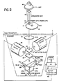
- FIG. 2 shows in schematic form a scanning apparatus 10 for scanning a film negative.
- the apparatus includes a disk member 12, for holding an original which is a photographic film negative 14.
- the film negative 14 is illuminated by light from a lamp mounted in a lamp housing 16.
- the lamp contained in this housing can for example be a 600 Watt tungsten lamp and the housing can include an eliptical reflector for collimating light from the lamp.
- a tapered integrating bar 18 along with a fiber optic face plate 20 produces diffused light (for scratch suppression). Light which passes through the negative is collected by a lens 22 and focused upon the surface of three area image sensors 24, 26 and 28.
- a beam splitter 29 is disposed between the lens 22 and sensors 24, 26, and 28.
- the beam splitter 29 separates three colored light beams (red, green, and blue) from light which is transmitted through the negative 14 and make take a number of well-known forms.
- one conventional beam splitter (as illustrated in Figure 2) comprises three prism components-29a, 29b, and 29c.
- Prism 29a has a blue reflecting coating on the second surface encountered by the light beam. This surface is spaced from the second prism 29b by a small air gap so as to enhance the reflection of blue light.
- the second prism 29b and the third prism 29c are cemented at their interface with the inclusion of a metallic coating such as Inconel @ (Reg. Trademark of International Nickel Company) between the second and third prism.
- the coating is not intended to provide color separation but instead reflects and transmits equal amounts of red and green light.
- Prism trim filters 24a, 26a, and 28a transmit separate red, green, and blue light beam images with the required spectral makeup to the respective area image sensors 24, 26, and 28. Each of these colored light beams forms a particular colored light image (or real image) of the film negative 14 which is focused on its sensor.
- Image displacement is independent of the axial position of the glass plates or the lens focal length, which is not the case when a mirror is used for image displacement.
- Rotation of the glass plate 32 about an axis of rotation translates the light image in the y-scan direction across the surface of each of the three area image sensors 24, 26 and 28 respectively.
- rotation of the glass plate 30 about an axis of rotation causes translational movement of the light image in the x direction (orthogonal to the y direction) along the surface of each of the three area image sensors.
- a first stepper motor 34 is adapted to incrementally rotate glass plate 30 and a second stepper motor 36 is adapted to incrementally rotate glass plate 32.
- These stepper motors are each under the control of a stepper motor controller 46.
- a microprocessor ( ⁇ /p) 50 provides stepper motor control signals to the separate motor controller 46. Rather than stepper motors, a servo-control system could be used to move the glass plates.
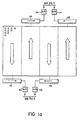
- FIGs 1a and 1b schematically show the general organization of an area image sensor having a sparse array of sensor elements which can be used in accordance with the invention.
- Several of the sensor elements which are shown in Figure 1b are identified as A, B, C, D, E, F, G, H and I.
- the elements are arranged in columns. Between each column there are conventional interline CCD shift registers 51.
- each of the sensor elements samples a different pixel of the light image of the negative 14.
- the origin is at the upper left hand position of that portion of the light image of the original from which the sensor will sample light image pixels. This coordinate system is shown in Figure 3a.
- the microprocessor 50 delivers a signal to stepper controller 46 for stepper motor 34, which rotates plate 30 an increment so as to laterally translate the light image in the x direction an amount so that each element is now at its light image position (2, 1) and samples light image pixel 2.
- stepper motor 34 is again energized and incremented so that all of the elements sample their corresponding light image pixel 3; this continues to position 12.
- the stepper motor 36 however must be energized while motor 34 is not energized.
- the light image will be incrementally moved layerally in only the y direction. Subsequent incremental energization of stepper motor 34 will result in the sampling of image pixels 13 thru 24. Once again, motor 36 must be energized to sample pixel 25. Pixels 25 thru 36 are sampled by the subsequent incremental energization of motor 34.
- Each sensor element thus samples thirty-six (36) different light image pixels.
- the light image pixels sampled form a block of 36 pixels organized in a rectangular 12x3 pattern.
- Figure 1d shows the identical arrangement of Figure 1c. However, the pixels sampled by element Are labelled "a”. Similarly sensor B sensed pixels are labelled "b” and sensor C sensed pixels are labelled "c".
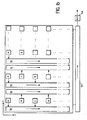
- Figures 1e-1g show improved sampling patterns according to the present invention, in which this problem is solved.
- each sensor again samples 36 light image pixels.
- Stepper motor 34 and 36 are selectively incrementally energized by ⁇ /p50.
- sequence sensor A senses the following positions (x, y) of the light image: (1,1), (1.2), (1,3), (2,4), (2,5), (2,6), (3,7), (3,8), (3, 9), (4, 9), (4, 8), (4, 7), (5, 6), (5, 5), (5, 4), (6, 3), (6, 2), (6, 1), (7, 1), (7, 2), (7, 3), (8,4), (8, 5), (8, 6), (9, 7), (9, 8), (9, 9), (10, 9), (10, 8), (10, 7), (11, 6), (11, 5), (11, 4), (12, 3), (12, 2) and (12,1).
- Figures 1e-g show only three representative sampling patterns or dither schemes which guarantee that every digital pixel has a neighbor scanned by a different element. Other patterns will suggest themselves to those skilled in the art. With any of these patterns, the loss of a single element will not cause substantial degradation of an output image.
- At the edges of a digital image there are pixels without a next-nearest neighbor produced by another sensor, and, along the top edge where there are holes.
- a hole is a pixel position which. has not been sampled by a sensor element. One can either trim the edges and/or fill the top edge holes with neighboring values.
- An example of a hole is at position (1, 3) of Figure 1e. It should be noted that the pattern of Figure 1g minimizes the number of holes.
- each area image sensor could be comprised of a sparse array of either photodiodes or capacitor elements.
- the photocharge which is accumulated in either a photodiode or a photocapacitor is transferred to an interline CCD shift register 51.
- the shift registers 51 conveniently can be constructed as a buried channel two phase device.
- each shift register 51 will be under the control of a plurality of electrodes (not shown).
- a potential is applied to an electrode opposite an element, a depletion region is formed under that electrode.
- an area image sensor which is formed with a p-substrate covered with a silicon dioxide layer on which there has been deposited a row of closely spaced electrodes for operating a shift register 51.
- a positive potential is applied to any one of the electrodes, it repels the holes into the substrate. Lattice electrons are exposed and a depletion region is formed.
- the potential profile of the depletion region is referred to as a well.
- Negative charge is of course accumulated under each element. After an adjacent well in a shift register is formed, and assuming the well is deeper than the charge region under the element, electrons will flow into the well of the shift register where they are free to move about but cannot penetrate the potential walls of the well. The potential profile (voltage) on the different electrodes of the shift register are now changed so that charge can be simultaneously shifted down each vertical shift register into four separate horizontal readout shift registers.
- each horizontal readout shift register 53 As shown in Figure 1a for each image area sensor, the output data rate can be greatly reduced; it is in fact, divided by four.
- the four large arrows shown in Figure 1a indicate the direction of signal transfer from a sensor to the horizontal shift registers 53 and the smaller arrows indicate the direction of charge transfer through the horizontal shift registers 53.
- Each horizontal register 53 is directly connected to its own analog-to-digital converter 54.
- the light image of a negative which is sampled by the elements of the area image sensors can be considered to be a two-dimensional light intensity function f (x, y), where x and y denote spatial coordinates and the digital value of the function at any point (x, y) is proportional to the brightness or gray level of the image pixel which was sampled.
- a digital image corresponding to a light image of a photographic negative is stored in a memory plane of a frame store 60.
- the memory plane is made up of a plurality of dynamic RAMs.
- the row and column numbers, x, y spatially identify a digital pixel.
- the value stored represents brightness or gray scale. In this case, for each digital image pixel 24 bits are stored; 8 bits gray scale for red, 8 bits gray scale for green and 8 bits for blue.
- a single A/D converter 54 is connected to the output port of each sensor horizontal shift register 53. As shown there are twelve A/D converters 54. Each A/D converter 54 is an 8 bit digitizer (256 gray levels).
- the microprocessor 50 provides the control signals to the stepper motor controller 46, timing generator 56 which provides timing signals to the image area sensors 24, 26 and 28, the A/D converters 54 and correction circuits 55.
- a correction circuit 55 is connected to each A/D converter 54 and will be understood to correct digital signal levels for sensor photosensitive errors.
- Timing generator 56 also provides timing signals to a frame store controller 58 and an output sequencer 64.
- a new 24 bit signal (3x8) is formed which represents red, green and blue levels.
- the frame store controller 58 provides a control signal to an x/y lookup table 62.
- Table 62 produces an address (x, y) which represents the location of the digital image pixel in the memory plane.
- the lookup table 62 causes each digitized image pixel (24 bits) to be stored in a particular cell in the memory plane corresponding to the location of the photographic negative from which the color information was scanned. When all of the cells of a memory plane are filled, a digital image is produced.
- An output sequencer 64 is also under the control of the frame store control logic 58. It produces an address (x, y) for reading out a digital image pixel having color information content.
- An output buffer 68 sequentially stores digital image pixel data from a digital image. It will be understood that the control signals provided by logic associated with lookup table 62 provide refresh signals to the memory plane RAMs and also an enable signal which permits digital pixel information to be read into memory.
- the output sequencer 64 provides control signals which enable output digital pixels to be read out from a digital image in a memory plane.
- the output buffer 68 delivers digital image pixel data to a digital image processor 70.
- the purpose of the digital image processor is to process a digital image so that a printer 80 will produce an output print which is more suitable for viewing than if processing had not taken place. It may function in accordance with image enhancing algorithms to achieve grain suppression, edge enhancement and tone scane enhancement. Examples of digital image processing algorithms are set forth in commonly assigned U.S. Patent Nos. 4,399,461, 4,442,454, and 4,446,484. Also an example of a printer 80, would be a laser printer.
- the image processor also will be understood to include an aglorithm which will replace a digital image pixel produced by a defective sensor element.
- the algorithm will substitute the value of a digital image pixel produced by a nearest neighbor by an effective sensor element.
- each area image sensor has an array of 60,000 elements.
- the 60,000 active elements on each sensor integrate the light transmitted by 60,000 light image pixels on the negative.
- the integrated charges are transferred to the shift registers 51 and the glass plates 30, and 32 are selectively rotated to new positions.
- the charge packets are transferred out for processing via the vertical 51 and horizontal shift registers 53.
- the charge packets are digitized and transferred to the appropriate location in a memory plane. Simultaneously 60,000 new pixels are being integrated. After each element makes 36 samples, 2.16 million digital pixels for each sensor will have been produced and a high resolution digital image with color information content will have been formed in a memory plane.
- the data rate in pixels (charge packets) per second is or about 22x10 6 pixels/s. At this data rate, there is a high likelihood of signal distortion. By using four separate output shift registers, the data is reduced from 22 MHz to 5.4 MHz. Digital pixels can be processed at this rate without distortion.
- Apparatus for efficiently forming a digital image from a photographic negative is useful as a product, for example, in an output laser printer which makes prints from negatives.
- the apparatus which uses an area image sensor having a matrix of elements, has the advantage to permit well-known techniques to be used to provide high quality output images when a sensor element becomes defective (drops out).
- correction algorithms can be designed to replace defective digital image pixels with their nearest neighbors which are more simplified than algorithms which have to replace defective digital pixels with their next-nearest neighbors.
- Sensitivity pattern noise is the variability from element-to-element in the sensitivity of sensor elements.
Landscapes
- Engineering & Computer Science (AREA)
- Multimedia (AREA)
- Signal Processing (AREA)
- Image Input (AREA)
Abstract
Claims (6)
ledit appareil étant caractérisé en ce que lesdits moyens (30, 34, 36) déplacent l'image lumineuse par rapport au capteur selon un modèle tel, que les pixels de l'image numérique produite par les éléments de détection aient au moins un de leurs pixels voisins les plus proches produit par un élément de capteur différent et en ce qu'il comprend en plus des moyens de compensation qui, dans le cas d'un élément défectueux, utilisent la sortie du signal de ce pixel voisin le plus proche produit par l'élément de capteur différent pour remplacer ledit élément défectueux.
ledit procédé étant caractérisé en ce que l'on déplace l'image lumineuse par rapport au capteur selon un modèle tel que les pixels de l'image numérique produite par les éléments de détection ont au moins un de leurs pixels voisins les plus proches produit par un élément de capteur différent, et en ce que dans l'hypothèse d'un élément défectueux, on utilise la sortie de signal de ce pixel voisin le plus proche produit par élément de détection différent pour remplacer ledit élément défectueux.
Applications Claiming Priority (4)
| Application Number | Priority Date | Filing Date | Title |
|---|---|---|---|
| US71024285A | 1985-03-11 | 1985-03-11 | |
| US710206 | 1985-03-11 | ||
| US710242 | 1985-03-11 | ||
| US06/710,206 US4638371A (en) | 1985-03-11 | 1985-03-11 | Multiple exposure of area image sensor having a sparse array of elements |
Publications (2)
| Publication Number | Publication Date |
|---|---|
| EP0215847A1 EP0215847A1 (fr) | 1987-04-01 |
| EP0215847B1 true EP0215847B1 (fr) | 1990-04-18 |
Family
ID=27108393
Family Applications (1)
| Application Number | Title | Priority Date | Filing Date |
|---|---|---|---|
| EP19860901697 Expired EP0215847B1 (fr) | 1985-03-11 | 1986-02-27 | Procede et appareil de formation d'images numeriques |
Country Status (3)
| Country | Link |
|---|---|
| EP (1) | EP0215847B1 (fr) |
| DE (1) | DE3670552D1 (fr) |
| WO (1) | WO1986005641A1 (fr) |
Families Citing this family (15)
| Publication number | Priority date | Publication date | Assignee | Title |
|---|---|---|---|---|
| DE3837063C1 (fr) * | 1988-10-31 | 1990-03-29 | Reimar Dr. 8000 Muenchen De Lenz | |
| US5877807A (en) * | 1988-10-31 | 1999-03-02 | Lenz; Reimar | Optoelectronic colored image converter |
| JPH06350931A (ja) * | 1993-06-02 | 1994-12-22 | Hamamatsu Photonics Kk | 固体撮像装置 |
| WO1998003010A2 (fr) * | 1996-07-15 | 1998-01-22 | Pacific Title And Mirage, Inc. | Systeme rapide d'imagerie a haute resolution |
| US6786420B1 (en) | 1997-07-15 | 2004-09-07 | Silverbrook Research Pty. Ltd. | Data distribution mechanism in the form of ink dots on cards |
| US6618117B2 (en) | 1997-07-12 | 2003-09-09 | Silverbrook Research Pty Ltd | Image sensing apparatus including a microcontroller |
| US6690419B1 (en) | 1997-07-15 | 2004-02-10 | Silverbrook Research Pty Ltd | Utilising eye detection methods for image processing in a digital image camera |
| AUPO850597A0 (en) | 1997-08-11 | 1997-09-04 | Silverbrook Research Pty Ltd | Image processing method and apparatus (art01a) |
| US7110024B1 (en) | 1997-07-15 | 2006-09-19 | Silverbrook Research Pty Ltd | Digital camera system having motion deblurring means |
| US6624848B1 (en) | 1997-07-15 | 2003-09-23 | Silverbrook Research Pty Ltd | Cascading image modification using multiple digital cameras incorporating image processing |
| US6948794B2 (en) | 1997-07-15 | 2005-09-27 | Silverbrook Reserach Pty Ltd | Printhead re-capping assembly for a print and demand digital camera system |
| US6985207B2 (en) | 1997-07-15 | 2006-01-10 | Silverbrook Research Pty Ltd | Photographic prints having magnetically recordable media |
| US6879341B1 (en) | 1997-07-15 | 2005-04-12 | Silverbrook Research Pty Ltd | Digital camera system containing a VLIW vector processor |
| AUPP702098A0 (en) | 1998-11-09 | 1998-12-03 | Silverbrook Research Pty Ltd | Image creation method and apparatus (ART73) |
| AUPQ056099A0 (en) | 1999-05-25 | 1999-06-17 | Silverbrook Research Pty Ltd | A method and apparatus (pprint01) |
Family Cites Families (3)
| Publication number | Priority date | Publication date | Assignee | Title |
|---|---|---|---|---|
| JPS564286A (en) * | 1979-06-25 | 1981-01-17 | Canon Inc | Photoelectric converter |
| US4331979A (en) * | 1980-10-02 | 1982-05-25 | Rca Corporation | Line-scan still image reproducer |
| FR2539937B1 (fr) * | 1983-01-21 | 1986-11-07 | Thomson Csf | Dispositif photosensible a transfert de charge |
-
1986
- 1986-02-27 EP EP19860901697 patent/EP0215847B1/fr not_active Expired
- 1986-02-27 WO PCT/US1986/000399 patent/WO1986005641A1/fr active IP Right Grant
- 1986-02-27 DE DE8686901697T patent/DE3670552D1/de not_active Expired - Fee Related
Also Published As
| Publication number | Publication date |
|---|---|
| DE3670552D1 (de) | 1990-05-23 |
| WO1986005641A1 (fr) | 1986-09-25 |
| EP0215847A1 (fr) | 1987-04-01 |
Similar Documents
| Publication | Publication Date | Title |
|---|---|---|
| US4638371A (en) | Multiple exposure of area image sensor having a sparse array of elements | |
| EP0215847B1 (fr) | Procede et appareil de formation d'images numeriques | |
| EP0091798B1 (fr) | Capteur d'images à l'état solide | |
| EP0021096B1 (fr) | Dispositif de formation d'image pour produire des signaux électriques et son utilisation dans un appareil de fac-similé | |
| US4603356A (en) | Imaging system with light valve and photodetector | |
| CA1178726A (fr) | Imageur a points bilineaires adjacents | |
| JP2001169050A (ja) | 多数の異なるセンサ領域を有するフォトセンサアレイ | |
| US4712137A (en) | High density CCD imager | |
| JP2501656B2 (ja) | 画像走査装置 | |
| EP0490045B1 (fr) | Système capteur d'images en couleurs à analyse singulière, à retard de temps et à intégration | |
| US4775895A (en) | Modular image sensor structure | |
| CA1135833A (fr) | Dispositif pour le balayage d'images en couleurs | |
| EP0397669B1 (fr) | Scanner d'entree | |
| JP2985959B1 (ja) | カラ―撮像装置およびそれを用いた画像読み取り装置 | |
| EP0680203B1 (fr) | Système de balayage pour la prise ou la projection d'images | |
| EP0225027B1 (fr) | Génération électronique d'images | |
| CA1134498A (fr) | Dispositif pour balayer l'image en couleurs | |
| WO1986005642A1 (fr) | Appareil de balayage et d'echantillonnage d'images reelles | |
| US4066355A (en) | Solid-state color-copying scanner | |
| JPS6156913B2 (fr) | ||
| JPH0834566B2 (ja) | 放射センサの操作方法 | |
| US5079415A (en) | Apparatus for converting optical information into electrical information signal, information storage element and method for storing information in the information storage element | |
| EP0070620A2 (fr) | Dispositif de formation d'image à haute densité | |
| JPH0759097A (ja) | 多感光領域を有するカラー撮像電荷結合アレイ | |
| JPS62161255A (ja) | 画像読取装置 |
Legal Events
| Date | Code | Title | Description |
|---|---|---|---|
| PUAI | Public reference made under article 153(3) epc to a published international application that has entered the european phase |
Free format text: ORIGINAL CODE: 0009012 |
|
| AK | Designated contracting states |
Kind code of ref document: A1 Designated state(s): DE FR GB |
|
| 17P | Request for examination filed |
Effective date: 19870307 |
|
| 17Q | First examination report despatched |
Effective date: 19890223 |
|
| GRAA | (expected) grant |
Free format text: ORIGINAL CODE: 0009210 |
|
| AK | Designated contracting states |
Kind code of ref document: B1 Designated state(s): DE FR GB |
|
| PG25 | Lapsed in a contracting state [announced via postgrant information from national office to epo] |
Ref country code: FR Effective date: 19900418 |
|
| REF | Corresponds to: |
Ref document number: 3670552 Country of ref document: DE Date of ref document: 19900523 |
|
| EN | Fr: translation not filed | ||
| PLBE | No opposition filed within time limit |
Free format text: ORIGINAL CODE: 0009261 |
|
| STAA | Information on the status of an ep patent application or granted ep patent |
Free format text: STATUS: NO OPPOSITION FILED WITHIN TIME LIMIT |
|
| PG25 | Lapsed in a contracting state [announced via postgrant information from national office to epo] |
Ref country code: GB Effective date: 19910227 |
|
| 26N | No opposition filed | ||
| GBPC | Gb: european patent ceased through non-payment of renewal fee | ||
| PG25 | Lapsed in a contracting state [announced via postgrant information from national office to epo] |
Ref country code: DE Effective date: 19911101 |