EP0213342A2 - Programmierbarer Wecksignalgenerator - Google Patents
Programmierbarer Wecksignalgenerator Download PDFInfo
- Publication number
- EP0213342A2 EP0213342A2 EP86109547A EP86109547A EP0213342A2 EP 0213342 A2 EP0213342 A2 EP 0213342A2 EP 86109547 A EP86109547 A EP 86109547A EP 86109547 A EP86109547 A EP 86109547A EP 0213342 A2 EP0213342 A2 EP 0213342A2
- Authority
- EP
- European Patent Office
- Prior art keywords
- ring
- signal
- ringing
- output
- ring signal
- Prior art date
- Legal status (The legal status is an assumption and is not a legal conclusion. Google has not performed a legal analysis and makes no representation as to the accuracy of the status listed.)
- Withdrawn
Links
Images


Classifications
-
- H—ELECTRICITY
- H04—ELECTRIC COMMUNICATION TECHNIQUE
- H04M—TELEPHONIC COMMUNICATION
- H04M19/00—Current supply arrangements for telephone systems
- H04M19/02—Current supply arrangements for telephone systems providing ringing current or supervisory tones, e.g. dialling tone or busy tone
- H04M19/023—Current supply arrangements for telephone systems providing ringing current or supervisory tones, e.g. dialling tone or busy tone by reversing the polarity of the current at the exchange
Definitions
- the present invention generally relates to a digitally controlled ring signal generator and, in particular, relates to such a ring signal generator that is both inexpensive and simplistic in the implementation thereof.
- This object is accomplished, at least in part, by providing a complete ringing circuit without the use of bulky transformers or expensive commutating switches.
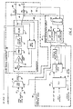
- each ringing circuit, 10 and 12 effectively function as buffer amplifiers that translate low level signals, received from a plurality of a.c. signal sources 16 and a d.c. signal source from the voltage generator 14, into high voltage/power signals required for telephone ringing.
- each ringing circuit, 10 and 12 provides ringing signals to a group of 30 subscriber lines/trunks by means of a common ring bus having the ringing circuits, 10 and 12, coupled thereto via lines, 18 and 20, respectively.
- Each ringing circuit, 10 and 12 provides, for example, one of four frequencies, f1, f2, f3, or f4, of a fixed amplitude superimposed upon a positive d.c. bias and provided to the ringing circuits, 10 and 12, under the control of a microprocessor interface bus 22.
- the d.c. bias can be any value greater than or equal to the peak amplitude of the reference voltage. This is ensured by maintaining Vpki less than Vdci, as shown in Figure 5.
- control signal on bus 22 is a logic signal and the specific programming, per se, of the microprocessor is not considered part of the present invention. It is also understood that the ringing circuits, 10 and 12, of the present invention can provide signals useful for purposes other than telephone ringing, per se, such as d.c. voltages for use in coin operated telephone controls.
- Each of the ring signal reference sources 16 provides a distinct a.c. signal of a particular frequency at the output thereof.
- This a.c. signal is d.c. biased by the d.c. voltage from a voltage generator 14 that is greater than or equal to the peak amplitude of the reference voltage from the ring signal reference sources 16. This condition is graphically illustrated in Figure 5 and must be satisfied in order to provide a substantially distortion free a.c. signal.
- the d.c. voltage generator 14 provides the d.c. biasing voltages and is discussed in greater detail hereinafter.
- a functional block diagram of the ringing circuit 10 is illustrated in Figure 2.
- An analog multiplexer 24, under microprocessor control, selects a ring reference source output sinusoidal signal on one of four input lines 26 (another line 28 is included for a d.c. signal input) and provides voltage reference signal on output line 30 to a ring signal generator 32, that functions as a d.c./d.c. flyback converter.
- the ring signal generator 32 includes a summer 34, an error amplifier 36, a pulse width modulator 38, a pulse limiter 40, a d.c. to d.c. converter 42 and a balanced attenuator 44.
- the ring signal generator 32 is described in more detail with reference to Figure 3.
- the ring signal generator 32 is coupled to the telephone subscriber tip and ring lines 18.
- a typical subscriber line connection is illustrated at 46.
- Resistors 48 and 50 function as current sensors and for current limiting and surge protection.
- the supervisory control signal on lines 52 and 54, coupled to ring supervisory circuit 56, are derived by sensing the current flow in the subscriber loop through sensing resistor 50, the current is then detected by buffer 58.
- the sensed signal coupled to buffer 58 may include only a.c. only or both a.c. and d.c. components.
- Subscriber Off-Hook signal (ring-trip) is obtained by filtering out the ac component and comparing the remaining d.c. signal with a reference d.c. signal derived directly from the signal source. This is preferably accomplished in ring supervision circuit 56, which is equivalent to a bridge circuit with high precision and insensitivity to source voltage variation.
- Ringing current presence detector 60 detects ring current in the subscriber loop from the output of buffer 58 by feeding the output signal to a peak detector circuit; the output of which peak detector is compared to a reference signal which defines the threshold for a positive current present condition.
- Ring trip detector circuit 62 detects ring-trip via line 64 and the output of buffer 58. Ring presence and ring-trip signals are coupled to the processor via termination control interface circuit 66, which provides the communication interface between the processor and the ring circuit and which is a portion of the ring circuit control logic 68.
- Control logic 70 checks the data integrity of the data instructions received by the termination control interface 66 from the processor, and energizes ring signal generator 32 upon receipt of a positive polarity signal.
- a security timer 72 limits the energization to about 2.5 seconds to protect the ringing circuit from damage which could result from a prolonged ringing interval caused, for example, by faulty data.
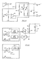
- ringing signal generator 32 To generate a ringing signal by energizing ringing circuit 106, the analog multiplexer 24 output, Vref, illustrated in Figure 5, is coupled to error amplifier 36 on line 30 with a feedback signal on the other input derived from the output Vs1 of a small d.c./d.c. converting ferrite pulse transformer 74.
- a 97.52 kHz sawtooth waveform is coupled to one input of comparator 76 and the output of amplifier 36 is coupled to the positive input of comparator 76, that functions as the pulse width modulator 38; the output being coupled to pulse limiter 40 and then to the gate of FET 78 for amplification prior to d.c./d.c. conversion by ferrite pulse transformer 74 to V1s.
- ring present detection circuit 60 Detection of Off-Hook causes an Off-Hook status signal to be coupled to the microprocessor and the initiation of ringing signal removal process. Ring removal is accomplished by changing Vref to zero.
- a command from the microprocessor to release the ring relay in the line circuit is obtained, achieving dry-switching.
- a similar shut-down procedure is implemented at the conclusion of each ringing interval.
- the ringing cadence i.e. the provision of a burst of ringing signal at a predetermined time interval, may be governed by processor software or other command origination, by turning ring circuit 32 ON and OFF at specific intervals.
- a preferred discharge circuit 80 in parallel with capacitor 82 is illustrated in Figure 4.
- the output of error amplifier 36 is coupled to one input of operational amplifier 84 that distributes the total discharge power between the transistors, 86 and 88.
- Transistor 90 has a -3 volt base bias having the collector thereof tied to the base of amplifier 86.
- the amplified output voltage V is discharged through capacitor 82 to provide a smooth discharge transition.
- the amount of discharging current is proportional to the error signal from amplifier 36.
- FIG. 6 A block diagram of a ring supervision circuit 56 is illustrated in Figure 6. Ringing voltage and current voltage is sensed across resistor 50 and coupled to ring-trip detector 62 via buffer 58 and attenuator 92, low pass filtered by filters 94 and 96 and coupled to the inputs of comparator 98; the output of comparator 98 being a logical ring-trip signal. Essentially, ring-trip is obtained by filtering out the a.c. components and comparing the remaining d.c. to a reference extracted from the source.
- Ring presence detector 60 detects tne presence of ringing current from the output of buffer 58, coupling the output of buffer 58 to a peak detector 100; the output thereof being compared in comparator 102 to a reference signal on line, that defines a threshold for a positive current present condition.
- a typical ring-trip detector 62 useful herewith is discussed and described in the aforementioned U.S. Patent No. 4,349,703.
- a typical control logic circuit 70 and security timer 72 is also shown and discussed therein. The only significant difference being that the control logic 70 as used herein would not require the square wave input f sq1 , f sq2 , f sq3 and f sq4 described therein.
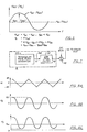
- a ring signal reference source 16 is illustrated in functional block diagramatic form in Figure 7.
- Figures 8(a), 8(b), and 8(c) illustrate various waveforms appearing at critical points in the block diagram of Figure 7 that are helpful in understanding the operation of the ring signal reference source 16.
- Triangular waveform generator 106 generates waveform V1 as an output on line 108, and passedthrough low pass felter 112 resulting in waveform V2 illustrated by waveform 8(b).
- Signal V2 is summed at summation node 110 with a d.c. bias signal and has a summed output V3, illustrated by waveform 8(c).
- Figure 9 illustrates a detailed schematic of the ring oscillator circuit including a triangle waveform generator 106 and low-pass filter 112 of Figure 7.
- Operational amplifiers, 114 and 116 are biased by resistors 118, 120, 122 and 124, and capacitor 126 generate V1 illustrated, at Figure 8(a), i.e. a triangular waveform having a peak amplitude of about 1.8 volts.
- the voltage at the output of operational amplifier 114 is a square wave having an amplitude defined by the saturation of the operational amplifiers, 114 and 116.
- Voltage V1 is coupled to the low-pass filter 112 at the positive going input of operational amplifier 128 biased by resistors 130, 132 and 134, and capacitors, 136 and 138.
- the output of operational amplifier 128 is V2 illustrated by Figure 8(b), which is a sine wave. Frequency adjustment is accomplished by varying resistor 120, the Q of filter 112 is 1.5873 with a center frequency determined by the values of the resistors, 124 and 130. The d.c. gain is 2.373, using exemplary values.
- Sine wave V2 is coupled to operational amplifier 140, biased via resistors, 142, 144, 146 and 148.
- the a.c. signal amplitude is adjustable via resistor 142 and the d.c. amplitude is adjustable via resistor 144.
- FIG 11 a schematic of a typical d.c. voltages generation circuit 14 shown in Figure 1 is illustrated.
- This circuit derives the various d.c. voltages needed for biasing the various components within the ringing signal generator and includes operational amplifiers 150, 152, and 154 that generate, respectively, the bias to discharger 80 on line 156, reference bias for coin voltage and bias to low level oscillators.
Applications Claiming Priority (2)
| Application Number | Priority Date | Filing Date | Title |
|---|---|---|---|
| US06/756,879 US4656659A (en) | 1985-07-18 | 1985-07-18 | Programmable ring signal generator |
| US756879 | 1985-07-18 |
Publications (2)
| Publication Number | Publication Date |
|---|---|
| EP0213342A2 true EP0213342A2 (de) | 1987-03-11 |
| EP0213342A3 EP0213342A3 (de) | 1988-11-30 |
Family
ID=25045442
Family Applications (1)
| Application Number | Title | Priority Date | Filing Date |
|---|---|---|---|
| EP86109547A Withdrawn EP0213342A3 (de) | 1985-07-18 | 1986-07-11 | Programmierbarer Wecksignalgenerator |
Country Status (5)
| Country | Link |
|---|---|
| US (1) | US4656659A (de) |
| EP (1) | EP0213342A3 (de) |
| JP (1) | JPS6221359A (de) |
| AU (1) | AU588896B2 (de) |
| BE (1) | BE905134A (de) |
Cited By (3)
| Publication number | Priority date | Publication date | Assignee | Title |
|---|---|---|---|---|
| US4897871A (en) * | 1980-04-04 | 1990-01-30 | Siemens Corporation | Apparatus for transmitting and/or receiving balanced signals on a two-wire telecommunication line |
| DE4218845A1 (de) * | 1992-06-09 | 1993-12-16 | Bosch Telecom | Schaltungsanordnung für einen Rufspannungsgenerator |
| WO2002032105A1 (en) * | 2000-10-13 | 2002-04-18 | Tellabs Oy | Method and circuit arrangement for detecting ring trip in a wireline telephone network |
Families Citing this family (21)
| Publication number | Priority date | Publication date | Assignee | Title |
|---|---|---|---|---|
| CA1247708A (en) * | 1985-10-28 | 1988-12-28 | Stanley D. Rosenbaum | Amplifier with double rail output |
| GB8606151D0 (en) * | 1986-03-12 | 1986-04-16 | Gen Electric Co Plc | Telephone system circuit |
| IT1213306B (it) * | 1986-07-29 | 1989-12-20 | Sgs Microelettronica Spa | Circuito telefonico, integrabile monoliticamente, per l'invio disegnali di suoneria in una linea telefonica d'utente e per il riconoscimento dello sgangio in fase di suoneria. |
| IT1197977B (it) * | 1986-11-13 | 1988-12-21 | Sgs Microelettronica Spa | Circuito telefonico, integrabile monoliticamente, per l'invio di segnali di suoneria in una linea telefonica d'utente ed il riconoscimento dello sgancio in fase di suoneria |
| KR900008817A (ko) * | 1988-11-30 | 1990-06-04 | 안시환 | 교환시스템에서의 자동적인 링 부하 균등 배분방법 |
| US4924511A (en) * | 1988-12-16 | 1990-05-08 | Siemens Transmission Systems, Inc. | Ring signal generator for generating ring signals of different frequencies and power levels in response to user selection |
| US4908857A (en) * | 1989-05-22 | 1990-03-13 | Siemens Transmission Systems, Inc. | Isolated drive circuit |
| US4965692A (en) * | 1989-07-31 | 1990-10-23 | Siemens Transmission Systems, Inc. | Overload detector and protection circuit |
| US5001748A (en) * | 1989-08-21 | 1991-03-19 | Siemens Transmission Systems, Inc. | Ringing signal generator |
| US4955053A (en) * | 1990-03-16 | 1990-09-04 | Reliance Comm/Tec Corporation | Solid state ringing switch |
| US5260996A (en) * | 1990-12-10 | 1993-11-09 | Reliance Comm/Tec Corporation | Current limited electronic ringing generator |
| US5140630A (en) * | 1991-05-01 | 1992-08-18 | Light Logic, Ltd. | Added main line apparatus |
| JP3189054B2 (ja) * | 1991-05-07 | 2001-07-16 | 富士通株式会社 | 加入者装置 |
| JPH0563798A (ja) * | 1991-08-30 | 1993-03-12 | Fujitsu Ltd | 呼出信号発生回路 |
| JP3056551B2 (ja) * | 1991-09-02 | 2000-06-26 | 富士通株式会社 | 加入者系伝送装置のアラーティングケーダンス制御方式 |
| US5307407A (en) * | 1991-12-19 | 1994-04-26 | Nec America, Inc. | 20 Hz ring generator using high frequency PWM control |
| JP3226617B2 (ja) * | 1992-08-20 | 2001-11-05 | 株式会社東芝 | ベル信号発生回路 |
| US6169800B1 (en) * | 1997-07-02 | 2001-01-02 | Motorola, Inc. | Integrated circuit amplifier and method of adaptive offset |
| US6289099B1 (en) * | 1998-11-30 | 2001-09-11 | Qualcomm Inc. | Ringer for satellite user terminals |
| US6690792B1 (en) * | 1999-11-19 | 2004-02-10 | Adtran Inc. | Active decoupling and power management circuit for line-powered ringing generator |
| US7847433B2 (en) * | 2007-11-27 | 2010-12-07 | Rain Bird Corporation | Universal irrigation controller power supply |
Citations (3)
| Publication number | Priority date | Publication date | Assignee | Title |
|---|---|---|---|---|
| EP0037111A1 (de) * | 1980-03-31 | 1981-10-07 | International Standard Electric Corporation | Schaltungsanordnung zur Erzeugung von Rufsignalen für Fernmeldeleitungen |
| WO1983000959A1 (en) * | 1981-09-03 | 1983-03-17 | Western Electric Co | Telephone line circuit |
| EP0075914A1 (de) * | 1981-09-28 | 1983-04-06 | Nec Corporation | Teilnehmeranschlussschaltung mit steuerbarem Gleichspannungswandler als Speiseschaltung |
Family Cites Families (2)
| Publication number | Priority date | Publication date | Assignee | Title |
|---|---|---|---|---|
| FR2371840A1 (fr) * | 1976-10-04 | 1978-06-16 | Ibm France | Circuit d'interface |
| MX150197A (es) * | 1980-03-31 | 1984-03-29 | Int Standard Electric Corp | Mejoras a sistema de senalizacion telefonica |
-
1985
- 1985-07-18 US US06/756,879 patent/US4656659A/en not_active Expired - Lifetime
-
1986
- 1986-07-08 AU AU59851/86A patent/AU588896B2/en not_active Ceased
- 1986-07-11 EP EP86109547A patent/EP0213342A3/de not_active Withdrawn
- 1986-07-18 JP JP61168186A patent/JPS6221359A/ja active Pending
- 1986-07-18 BE BE2/61018A patent/BE905134A/fr not_active IP Right Cessation
Patent Citations (3)
| Publication number | Priority date | Publication date | Assignee | Title |
|---|---|---|---|---|
| EP0037111A1 (de) * | 1980-03-31 | 1981-10-07 | International Standard Electric Corporation | Schaltungsanordnung zur Erzeugung von Rufsignalen für Fernmeldeleitungen |
| WO1983000959A1 (en) * | 1981-09-03 | 1983-03-17 | Western Electric Co | Telephone line circuit |
| EP0075914A1 (de) * | 1981-09-28 | 1983-04-06 | Nec Corporation | Teilnehmeranschlussschaltung mit steuerbarem Gleichspannungswandler als Speiseschaltung |
Cited By (3)
| Publication number | Priority date | Publication date | Assignee | Title |
|---|---|---|---|---|
| US4897871A (en) * | 1980-04-04 | 1990-01-30 | Siemens Corporation | Apparatus for transmitting and/or receiving balanced signals on a two-wire telecommunication line |
| DE4218845A1 (de) * | 1992-06-09 | 1993-12-16 | Bosch Telecom | Schaltungsanordnung für einen Rufspannungsgenerator |
| WO2002032105A1 (en) * | 2000-10-13 | 2002-04-18 | Tellabs Oy | Method and circuit arrangement for detecting ring trip in a wireline telephone network |
Also Published As
| Publication number | Publication date |
|---|---|
| AU5985186A (en) | 1987-01-22 |
| JPS6221359A (ja) | 1987-01-29 |
| US4656659A (en) | 1987-04-07 |
| EP0213342A3 (de) | 1988-11-30 |
| AU588896B2 (en) | 1989-09-28 |
| BE905134A (fr) | 1987-01-19 |
Similar Documents
| Publication | Publication Date | Title |
|---|---|---|
| US4656659A (en) | Programmable ring signal generator | |
| US4349703A (en) | Programmable ring signal generator | |
| US4092610A (en) | Modulated carrier amplifying system | |
| KR860002183A (ko) | 디지탈 오디오 증폭기 | |
| US4315107A (en) | Telephone range extender with gain | |
| US4370526A (en) | Arrangement for applying a ringing voltage to a subscriber's line | |
| US4631361A (en) | Programmable ring generator | |
| EP0440006B1 (de) | Verfahren und Vorrichtung zur Speisung einer Fernsprechleitung mit Gleichstrom | |
| US4152670A (en) | Signal generator, especially for ringing current in telecommunication system | |
| US4528425A (en) | Method of and circuitry for detecting, at a telephone exchange, the lifting of a subscriber's handset in response to ringing current emitted by the exchange | |
| EP0483088B1 (de) | Schaltung zur Erzeugung von Gebührenimpulsen zur Präsentation bei einem Fernsprechteilnehmer | |
| EP0092807B1 (de) | Digitale Überwachungsschaltung für ein Fernsprechsystem | |
| US4354062A (en) | Communication system signaling circuit | |
| US4761812A (en) | Constant power telephone line circuit | |
| US4092489A (en) | Switching arrangement for monitoring polarity reversal on lines in telecommunication systems | |
| US4515996A (en) | Telephone circuit | |
| SE447043B (sv) | Ringsignalgenerator | |
| CA1157595A (en) | Ringing signal supply | |
| US4133986A (en) | Subscriber's line equipment for a telephone exchange | |
| US4289933A (en) | Dial pulse detection | |
| EP0012762A1 (de) | Signalumsetzer mit rauschunterdrückung. | |
| CA1037565A (en) | Digital frequency shift-keyed transmitter | |
| US4435621A (en) | Speech direction detection circuits for telephone communication devices | |
| US4809258A (en) | Circuit arrangement for the indication of loop closure during the ringing condition | |
| US4178486A (en) | Ring sensing circuit for use with a service evaluation system |
Legal Events
| Date | Code | Title | Description |
|---|---|---|---|
| PUAI | Public reference made under article 153(3) epc to a published international application that has entered the european phase |
Free format text: ORIGINAL CODE: 0009012 |
|
| AK | Designated contracting states |
Kind code of ref document: A2 Designated state(s): CH DE FR GB IT LI NL |
|
| RAP1 | Party data changed (applicant data changed or rights of an application transferred) |
Owner name: ALCATEL N.V. |
|
| RAP3 | Party data changed (applicant data changed or rights of an application transferred) |
Owner name: ALCATEL N.V. |
|
| PUAL | Search report despatched |
Free format text: ORIGINAL CODE: 0009013 |
|
| AK | Designated contracting states |
Kind code of ref document: A3 Designated state(s): CH DE FR GB IT LI NL |
|
| STAA | Information on the status of an ep patent application or granted ep patent |
Free format text: STATUS: THE APPLICATION IS DEEMED TO BE WITHDRAWN |
|
| 18D | Application deemed to be withdrawn |
Effective date: 19890531 |
|
| RIN1 | Information on inventor provided before grant (corrected) |
Inventor name: CHEA, RAMON C. W., JR. |