EP0212817A1 - Wechselrichter - Google Patents
Wechselrichter Download PDFInfo
- Publication number
- EP0212817A1 EP0212817A1 EP86305157A EP86305157A EP0212817A1 EP 0212817 A1 EP0212817 A1 EP 0212817A1 EP 86305157 A EP86305157 A EP 86305157A EP 86305157 A EP86305157 A EP 86305157A EP 0212817 A1 EP0212817 A1 EP 0212817A1
- Authority
- EP
- European Patent Office
- Prior art keywords
- inverter circuit
- transformer
- circuit according
- switching means
- inverter
- Prior art date
- Legal status (The legal status is an assumption and is not a legal conclusion. Google has not performed a legal analysis and makes no representation as to the accuracy of the status listed.)
- Granted
Links
Images


Classifications
-
- H—ELECTRICITY
- H05—ELECTRIC TECHNIQUES NOT OTHERWISE PROVIDED FOR
- H05B—ELECTRIC HEATING; ELECTRIC LIGHT SOURCES NOT OTHERWISE PROVIDED FOR; CIRCUIT ARRANGEMENTS FOR ELECTRIC LIGHT SOURCES, IN GENERAL
- H05B41/00—Circuit arrangements or apparatus for igniting or operating discharge lamps
- H05B41/14—Circuit arrangements
- H05B41/26—Circuit arrangements in which the lamp is fed by power derived from dc by means of a converter, e.g. by high-voltage dc
- H05B41/28—Circuit arrangements in which the lamp is fed by power derived from dc by means of a converter, e.g. by high-voltage dc using static converters
- H05B41/295—Circuit arrangements in which the lamp is fed by power derived from dc by means of a converter, e.g. by high-voltage dc using static converters with semiconductor devices and specially adapted for lamps with preheating electrodes, e.g. for fluorescent lamps
-
- H—ELECTRICITY
- H02—GENERATION; CONVERSION OR DISTRIBUTION OF ELECTRIC POWER
- H02M—APPARATUS FOR CONVERSION BETWEEN AC AND AC, BETWEEN AC AND DC, OR BETWEEN DC AND DC, AND FOR USE WITH MAINS OR SIMILAR POWER SUPPLY SYSTEMS; CONVERSION OF DC OR AC INPUT POWER INTO SURGE OUTPUT POWER; CONTROL OR REGULATION THEREOF
- H02M7/00—Conversion of ac power input into dc power output; Conversion of dc power input into ac power output
- H02M7/42—Conversion of dc power input into ac power output without possibility of reversal
- H02M7/44—Conversion of dc power input into ac power output without possibility of reversal by static converters
- H02M7/48—Conversion of dc power input into ac power output without possibility of reversal by static converters using discharge tubes with control electrode or semiconductor devices with control electrode
- H02M7/53—Conversion of dc power input into ac power output without possibility of reversal by static converters using discharge tubes with control electrode or semiconductor devices with control electrode using devices of a triode or transistor type requiring continuous application of a control signal
- H02M7/537—Conversion of dc power input into ac power output without possibility of reversal by static converters using discharge tubes with control electrode or semiconductor devices with control electrode using devices of a triode or transistor type requiring continuous application of a control signal using semiconductor devices only, e.g. single switched pulse inverters
-
- Y—GENERAL TAGGING OF NEW TECHNOLOGICAL DEVELOPMENTS; GENERAL TAGGING OF CROSS-SECTIONAL TECHNOLOGIES SPANNING OVER SEVERAL SECTIONS OF THE IPC; TECHNICAL SUBJECTS COVERED BY FORMER USPC CROSS-REFERENCE ART COLLECTIONS [XRACs] AND DIGESTS
- Y02—TECHNOLOGIES OR APPLICATIONS FOR MITIGATION OR ADAPTATION AGAINST CLIMATE CHANGE
- Y02B—CLIMATE CHANGE MITIGATION TECHNOLOGIES RELATED TO BUILDINGS, e.g. HOUSING, HOUSE APPLIANCES OR RELATED END-USER APPLICATIONS
- Y02B70/00—Technologies for an efficient end-user side electric power management and consumption
- Y02B70/10—Technologies improving the efficiency by using switched-mode power supplies [SMPS], i.e. efficient power electronics conversion e.g. power factor correction or reduction of losses in power supplies or efficient standby modes
-
- Y—GENERAL TAGGING OF NEW TECHNOLOGICAL DEVELOPMENTS; GENERAL TAGGING OF CROSS-SECTIONAL TECHNOLOGIES SPANNING OVER SEVERAL SECTIONS OF THE IPC; TECHNICAL SUBJECTS COVERED BY FORMER USPC CROSS-REFERENCE ART COLLECTIONS [XRACs] AND DIGESTS
- Y10—TECHNICAL SUBJECTS COVERED BY FORMER USPC
- Y10S—TECHNICAL SUBJECTS COVERED BY FORMER USPC CROSS-REFERENCE ART COLLECTIONS [XRACs] AND DIGESTS
- Y10S315/00—Electric lamp and discharge devices: systems
- Y10S315/07—Starting and control circuits for gas discharge lamp using transistors
Definitions
- This invention relates to inverters and in particular to inverters for use with gas discharge lamps.
- Some gas discharge lamps exhibit a negative resistance characteristic when the gas in the lamp is ionized. This means that as current begins to increase through the lamp, the resistance of the lamp decreases. This resistance decrease causes the current to further increase and unless some current-limiting ballast means is provided, the lamp will be destroyed. A ballast system is therefore required which will enable the lamp to operate at a sufficiently high current for satisfactory illumination.
- iron core chokes have been used for ballast purposes, and the iron core ballast and starter switch circuit has been used to operate fluorescent lamps.
- Iron core ballasts do however have undesirable characteristics, such as, inter alia, low power efficiency, audible vibration, considerable weight, the requirement for a substantial amount of iron, light flicker and delayed starting.
- ballasts have become available. These offer increased power efficiency, no audible noise, less weight, less light flicker, instant starting and dimming. They consist of essentially an inverter that converts DC into high frequency AC. The high frequency AC drives a series resonant circuit in which the inductive component ballasts the fluorescent lamps. High striking voltages are generated by resonant magnification. There are two variations of this circuit. Self resonant inverters are the simplest and perhaps the most reliable but they cold strike the lamps and dimming can only be achieved by a reduction in the applied voltage. Driven inverters are capable of dimming and cathode preheat but their circuitry is complex, requiring feedback, protection and control. They are costly and have potential reliability problems.
- an inverter circuit comprising two input terminals for connecting a unidirectional current supply therebetween, two switching means connected in series across said input terminals, two secondary windings of a transformer, each arranged to control the operation of a respective switching means, a primary winding of the transformer having three connections of which the tap connection is to the junction of the two switching means, the other two being connected by parallel branches, the branches having, in one, bidirectional threshold means and, in the other, capacitive means, to an input of resonant circuit adapted to receive a load, and the output of the resonant circuit being connected via a first capacitor to one of said input terminals and via a second capacitor to the other of said input terminals, the arrangement being such that, in use, the switching means operate essentially alternately.
- an inverter circuit comprising two switching means arranged to operate alternately, each switching means controlled by means of a respective secondary winding of a transformer, a primary winding of the transformer having separate connections to capacitive means and bidirectional threshold means, the capacitive means and bidirectional threshold means being connected as parallel branches to an input of a resonant circuit adapted to receive a load.
- the bidirectional threshold means may be rectifiers or diodes arranged in a bridge formation having a forward voltage drop.
- the switching means may for example be transistors, each being protected by a respective unidirectional means such as a diode.
- Alternative switching means include MOSFETs or thyristors.
- Transformer is intended to include a conventional transformer or a similar device achieving the same effect.
- An inverter circuit according to the invention may further include a variable reactance in the branch including the capacitive means.
- a sub-circuit may be incorporated to regulate this reactance and thus to control the current drawn by the inverter.
- a gas discharge lamp control circuit including an inverter circuit as described in any of the five preceding paragraphs.
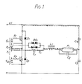
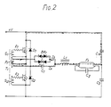
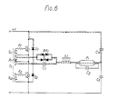
- Figures 1 to 6 show circuit paths in a self resonant inverter circuit according to the invention, used to control a gas discharge lamp
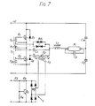
- Figure 7 shows an inverter further including a sub-circuit to control current drawn.
- this shows a gas discharge lamp F1 (the load), bridged by a capacitor C3, and an inductor L1 is connected to the input to the cathodes of the lamp.
- Capacitors C4 and C5 are connected is series across the unidirectional current supply.
- Transformer T1 has a primary winding P1 and two secondary windings S1 and S2. Each secondary winding is associated with and controls a respective switching means, for example transistors Q1 and Q2, connected to alternately switch the voltage applied to the circuit.
- the secondary windings of the transformer are connected to Q1 and Q2 via resistors R1 and R2.
- Each of the transistors is shunted by an associated diode (D1 or D2) to protect it from the inductive charge of the inductor L1.
- the primary P1 of the transformer has a tap input with tappings arranged feeding parallel branches to inductor L1, the other end of L1 being connected to gas discharge lamp F1.
- a first branch incorporates capacitive means, in this case a capacitor C1.
- a second branch incorporates bidirectional threshold means preferably in the form of a bridge arrangement BR1 having a forward voltage drop.
- Figure 4 shows Q2 conducting current I A and BR1 is no longer conducting. This is similar to the situation shown in figure 1 with Q1 conducting.
- Figure 5 shows currents I A and I B flowing through the capacitive means and bidirectional threshold means respectively. The total current I through the inductor L1 is I A + I B .
- Figure 6 shows D1 conducting the inductive charge from L1, the situation being similar to that shown in Figure 3. The cycle is then repeated with transistors Q1 and Q2 alternately switching on and off.
- the inverter's current may be varied by changing the effective capacitance of C1.
- this shows a capacitive branch being in the form of a first capacitor C1 and a second capacitor C2 arranged in parallel with one another, with the C2 arm incorporating a variable reactance, in this case a primary winding P2 of a transformer T2, for control purposes.
- primary winding P2 of T2 represents a high reactance in series with capacitor C2 and thus limits the current flow to C2.
- the reactance provided by primary P2 is decreased and thus by providing an adjunct control circuit 1 to control the current through the secondary winding, the reactance of the first and hence the current drawn by capacitor C2 can be controlled.
- the particular control circuit illustrated includes switch Q3, resistors R3, R4 and R5 and bridge BR2).
- Capacitor C2 has preferably about ten times the capacitance of capacitor C1 and thus in operation draws more current and takes a longer period to change to the forward voltage drop of the bidirectional threshold means BR1.
- the control circuit 1 When the inverter is first turned on, the control circuit 1 is arranged to gradually load the secondary winding of transformer T2.
- the current drawn by the capacitors can thus be gradually increased from a minimum level set essentially by C1 to a maximum level determined by the combined capacitance of capacitors C1 and C2.
- the minimum current drawn at the outset provides a preheat to the cathodes of the lamp. As this current is increased, the cathodes are further heated and the frequency approaches the resonant frequency so the voltage across the lamp increases and the lamp is struck. Dimming of the lamp can be achieved by operation of the control sub-circuit 1 to alter the reactance in the capacitive branch.
- circuits are possible.
- a full bridge inverter could be used.
- bidirectional conducting means having a forward voltage drop may be utilised.
- the capacitive branch need not have two capacitive arms and the means for developing at least an initial reactance in the capacitive arm could be by way of a variable resistor, particularly where the control sub-circuit is not required.
- the load may of course be other than a gas discharge lamp, and alternative switching means may be used.
Applications Claiming Priority (2)
| Application Number | Priority Date | Filing Date | Title |
|---|---|---|---|
| NZ212682 | 1985-07-08 | ||
| NZ212682A NZ212682A (en) | 1985-07-08 | 1985-07-08 | Self resonant inverter as electronic ballast for discharge lamp |
Publications (2)
| Publication Number | Publication Date |
|---|---|
| EP0212817A1 true EP0212817A1 (de) | 1987-03-04 |
| EP0212817B1 EP0212817B1 (de) | 1991-09-18 |
Family
ID=19921269
Family Applications (1)
| Application Number | Title | Priority Date | Filing Date |
|---|---|---|---|
| EP86305157A Expired - Lifetime EP0212817B1 (de) | 1985-07-08 | 1986-07-03 | Wechselrichter |
Country Status (6)
| Country | Link |
|---|---|
| US (1) | US4722040A (de) |
| EP (1) | EP0212817B1 (de) |
| AU (1) | AU587473B2 (de) |
| DE (1) | DE3681532D1 (de) |
| NZ (1) | NZ212682A (de) |
| ZA (1) | ZA865018B (de) |
Cited By (1)
| Publication number | Priority date | Publication date | Assignee | Title |
|---|---|---|---|---|
| US6229270B1 (en) | 1997-07-29 | 2001-05-08 | Indigitale Limited | Variable high frequency lamp controllers and systems |
Families Citing this family (5)
| Publication number | Priority date | Publication date | Assignee | Title |
|---|---|---|---|---|
| US4983887A (en) * | 1986-10-10 | 1991-01-08 | Nilssen Ole K | Controlled series-resonance-loaded ballast |
| KR920001705Y1 (ko) * | 1990-01-19 | 1992-03-09 | 이상우 | 형광등의 점등장치 |
| US5173643A (en) * | 1990-06-25 | 1992-12-22 | Lutron Electronics Co., Inc. | Circuit for dimming compact fluorescent lamps |
| FI87412C (fi) * | 1991-02-25 | 1992-12-28 | Kemppi Oy | Svetsningsinverter och foerfarande foer styrning av svetsningsinverter |
| US5291101A (en) * | 1992-07-28 | 1994-03-01 | Micro Technology, Inc. | Electronic ballast for a discharge lamp with current sensing |
Citations (3)
| Publication number | Priority date | Publication date | Assignee | Title |
|---|---|---|---|---|
| US4188661A (en) * | 1979-02-23 | 1980-02-12 | Gte Sylvania Incorporated | Direct drive ballast with starting circuit |
| FR2488477A1 (fr) * | 1980-08-05 | 1982-02-12 | Accumulateurs Fixes | Dispositif pour l'amorcage d'un tube fluorescent alimente par une source de tension a frequence elevee |
| US4525649A (en) * | 1982-07-12 | 1985-06-25 | Gte Products Corporation | Drive scheme for a plurality of flourescent lamps |
Family Cites Families (7)
| Publication number | Priority date | Publication date | Assignee | Title |
|---|---|---|---|---|
| JPS6011545B2 (ja) * | 1977-07-05 | 1985-03-26 | ソニー株式会社 | 自励式dc−dcコンバ−タ用の発振トランス |
| US4439819A (en) * | 1978-01-16 | 1984-03-27 | Rockwell International | Switching regulator with controlled simulated load |
| US4319316A (en) * | 1979-10-31 | 1982-03-09 | Gould Advance Limited | Controlled power supply apparatus |
| US4424556A (en) * | 1981-08-13 | 1984-01-03 | Matsushita Electric Industrial Co., Ltd. | Self-oscillating DC to DC converter |
| AU555174B2 (en) * | 1981-09-18 | 1986-09-18 | Oy Helvar | Electronic ballast for a discharge lamp |
| US4532456A (en) * | 1982-07-12 | 1985-07-30 | Gte Products Corporation | Output circuit for an electronic ballast system |
| FI68935C (fi) * | 1983-09-06 | 1985-11-11 | Helvar Oy | Inverterkrets med en regleringskrets foer att effektivera transistorernas styrning till ett slutarlaege |
-
1985
- 1985-07-08 NZ NZ212682A patent/NZ212682A/xx unknown
-
1986
- 1986-07-03 EP EP86305157A patent/EP0212817B1/de not_active Expired - Lifetime
- 1986-07-03 DE DE8686305157T patent/DE3681532D1/de not_active Expired - Lifetime
- 1986-07-07 ZA ZA865018A patent/ZA865018B/xx unknown
- 1986-07-07 US US06/882,178 patent/US4722040A/en not_active Expired - Fee Related
- 1986-07-08 AU AU59829/86A patent/AU587473B2/en not_active Ceased
Patent Citations (3)
| Publication number | Priority date | Publication date | Assignee | Title |
|---|---|---|---|---|
| US4188661A (en) * | 1979-02-23 | 1980-02-12 | Gte Sylvania Incorporated | Direct drive ballast with starting circuit |
| FR2488477A1 (fr) * | 1980-08-05 | 1982-02-12 | Accumulateurs Fixes | Dispositif pour l'amorcage d'un tube fluorescent alimente par une source de tension a frequence elevee |
| US4525649A (en) * | 1982-07-12 | 1985-06-25 | Gte Products Corporation | Drive scheme for a plurality of flourescent lamps |
Cited By (1)
| Publication number | Priority date | Publication date | Assignee | Title |
|---|---|---|---|---|
| US6229270B1 (en) | 1997-07-29 | 2001-05-08 | Indigitale Limited | Variable high frequency lamp controllers and systems |
Also Published As
| Publication number | Publication date |
|---|---|
| AU587473B2 (en) | 1989-08-17 |
| DE3681532D1 (de) | 1991-10-24 |
| ZA865018B (en) | 1987-05-27 |
| US4722040A (en) | 1988-01-26 |
| AU5982986A (en) | 1987-01-15 |
| EP0212817B1 (de) | 1991-09-18 |
| NZ212682A (en) | 1989-11-28 |
Similar Documents
| Publication | Publication Date | Title |
|---|---|---|
| US5841239A (en) | Circuit for dimming compact fluorescent lamps | |
| US5444333A (en) | Electronic ballast circuit for a fluorescent light | |
| US5144205A (en) | Compact fluorescent lamp dimming system | |
| US5148087A (en) | Circuit for driving a gas discharge lamp load | |
| US6023132A (en) | Electronic ballast deriving auxilliary power from lamp output | |
| US4914558A (en) | Series resonant inverter and method of lamp starting | |
| US5225742A (en) | Solid state ballast for high intensity discharge lamps | |
| US4958107A (en) | Switching arrangement for HID lamps | |
| EP0205287A2 (de) | Verbessertes Schaltnetzteil | |
| US5012161A (en) | Power factor correction circuit | |
| US5233270A (en) | Self-ballasted screw-in fluorescent lamp | |
| EP0171108A1 (de) | Wechselrichter zum Speisen eines Metalldampfentladungsrohrs | |
| US5825137A (en) | Electronic ballasts for plural lamp fluorescent lighting without feedback circuitry | |
| US5047690A (en) | Inverter power supply and ballast circuit | |
| US5341067A (en) | Electronic ballast with trapezoidal voltage waveform | |
| US4983887A (en) | Controlled series-resonance-loaded ballast | |
| US6211625B1 (en) | Electronic ballast with over-voltage protection | |
| EP0212817B1 (de) | Wechselrichter | |
| WO1996031092A1 (en) | Power system with simplified, low cost self-starting self oscillator, power factor correction, power regulation and output open circuit voltage regulation, overload and short circuit protection | |
| US5229690A (en) | Apparatus for operating discharge lamps utilizing a capacitor and charging circuit | |
| EP0126556A1 (de) | Verfahren zum Starten und Steuern einer Gasentladelampe, sowie Stromzufuhr und elektronischer Ballast dafür | |
| US4330736A (en) | Compensated current feedback oscillator ballast for fluorescent lamps and the like | |
| JPH04249892A (ja) | ガス放電ランプを動作させる電力回路 | |
| US6211619B1 (en) | Electronic ballast cathode heating circuit | |
| EP0223293A1 (de) | Stromversorgungsschaltung |
Legal Events
| Date | Code | Title | Description |
|---|---|---|---|
| PUAI | Public reference made under article 153(3) epc to a published international application that has entered the european phase |
Free format text: ORIGINAL CODE: 0009012 |
|
| AK | Designated contracting states |
Kind code of ref document: A1 Designated state(s): DE FR GB IT NL |
|
| 17P | Request for examination filed |
Effective date: 19870820 |
|
| 17Q | First examination report despatched |
Effective date: 19890511 |
|
| GRAA | (expected) grant |
Free format text: ORIGINAL CODE: 0009210 |
|
| AK | Designated contracting states |
Kind code of ref document: B1 Designated state(s): DE FR GB IT NL |
|
| ITF | It: translation for a ep patent filed |
Owner name: FUMERO BREVETTI S.N.C. |
|
| REF | Corresponds to: |
Ref document number: 3681532 Country of ref document: DE Date of ref document: 19911024 |
|
| ET | Fr: translation filed | ||
| PLBE | No opposition filed within time limit |
Free format text: ORIGINAL CODE: 0009261 |
|
| STAA | Information on the status of an ep patent application or granted ep patent |
Free format text: STATUS: NO OPPOSITION FILED WITHIN TIME LIMIT |
|
| 26N | No opposition filed | ||
| PGFP | Annual fee paid to national office [announced via postgrant information from national office to epo] |
Ref country code: FR Payment date: 19960426 Year of fee payment: 11 |
|
| PGFP | Annual fee paid to national office [announced via postgrant information from national office to epo] |
Ref country code: GB Payment date: 19960717 Year of fee payment: 11 |
|
| PGFP | Annual fee paid to national office [announced via postgrant information from national office to epo] |
Ref country code: NL Payment date: 19960731 Year of fee payment: 11 |
|
| PGFP | Annual fee paid to national office [announced via postgrant information from national office to epo] |
Ref country code: DE Payment date: 19960927 Year of fee payment: 11 |
|
| PG25 | Lapsed in a contracting state [announced via postgrant information from national office to epo] |
Ref country code: GB Free format text: LAPSE BECAUSE OF NON-PAYMENT OF DUE FEES Effective date: 19970703 |
|
| PG25 | Lapsed in a contracting state [announced via postgrant information from national office to epo] |
Ref country code: NL Free format text: LAPSE BECAUSE OF NON-PAYMENT OF DUE FEES Effective date: 19980201 |
|
| GBPC | Gb: european patent ceased through non-payment of renewal fee |
Effective date: 19970703 |
|
| PG25 | Lapsed in a contracting state [announced via postgrant information from national office to epo] |
Ref country code: FR Free format text: LAPSE BECAUSE OF NON-PAYMENT OF DUE FEES Effective date: 19980331 |
|
| NLV4 | Nl: lapsed or anulled due to non-payment of the annual fee |
Effective date: 19980201 |
|
| PG25 | Lapsed in a contracting state [announced via postgrant information from national office to epo] |
Ref country code: DE Free format text: LAPSE BECAUSE OF NON-PAYMENT OF DUE FEES Effective date: 19980401 |
|
| REG | Reference to a national code |
Ref country code: FR Ref legal event code: ST |
|
| PG25 | Lapsed in a contracting state [announced via postgrant information from national office to epo] |
Ref country code: IT Free format text: LAPSE BECAUSE OF NON-PAYMENT OF DUE FEES;WARNING: LAPSES OF ITALIAN PATENTS WITH EFFECTIVE DATE BEFORE 2007 MAY HAVE OCCURRED AT ANY TIME BEFORE 2007. THE CORRECT EFFECTIVE DATE MAY BE DIFFERENT FROM THE ONE RECORDED. Effective date: 20050703 |