EP0210436B1 - Verfahren zur Metallisierung von Keramik - Google Patents
Verfahren zur Metallisierung von Keramik Download PDFInfo
- Publication number
- EP0210436B1 EP0210436B1 EP19860108643 EP86108643A EP0210436B1 EP 0210436 B1 EP0210436 B1 EP 0210436B1 EP 19860108643 EP19860108643 EP 19860108643 EP 86108643 A EP86108643 A EP 86108643A EP 0210436 B1 EP0210436 B1 EP 0210436B1
- Authority
- EP
- European Patent Office
- Prior art keywords
- bath
- activator
- temperature
- catalyst
- chemical
- Prior art date
- Legal status (The legal status is an assumption and is not a legal conclusion. Google has not performed a legal analysis and makes no representation as to the accuracy of the status listed.)
- Expired - Lifetime
Links
- 238000000034 method Methods 0.000 title claims abstract description 26
- 230000008569 process Effects 0.000 title abstract description 8
- 229910010293 ceramic material Inorganic materials 0.000 title 1
- 239000000919 ceramic Substances 0.000 claims abstract description 32
- 239000010949 copper Substances 0.000 claims abstract description 16
- 229910052802 copper Inorganic materials 0.000 claims abstract description 13
- 239000000126 substance Substances 0.000 claims abstract description 13
- RYGMFSIKBFXOCR-UHFFFAOYSA-N Copper Chemical compound [Cu] RYGMFSIKBFXOCR-UHFFFAOYSA-N 0.000 claims abstract description 12
- 239000012190 activator Substances 0.000 claims abstract description 10
- 239000003054 catalyst Substances 0.000 claims abstract description 7
- 238000007747 plating Methods 0.000 claims abstract description 5
- 239000002243 precursor Substances 0.000 claims description 8
- 239000000853 adhesive Substances 0.000 claims description 7
- 238000007788 roughening Methods 0.000 claims description 6
- 150000001875 compounds Chemical class 0.000 claims description 5
- 239000011248 coating agent Substances 0.000 claims description 4
- 238000000576 coating method Methods 0.000 claims description 4
- 229910052763 palladium Inorganic materials 0.000 claims description 4
- 229910052697 platinum Inorganic materials 0.000 claims description 4
- 239000002253 acid Substances 0.000 claims description 3
- 229910001854 alkali hydroxide Inorganic materials 0.000 claims description 3
- 150000008044 alkali metal hydroxides Chemical class 0.000 claims description 3
- BIGPRXCJEDHCLP-UHFFFAOYSA-N ammonium bisulfate Chemical compound [NH4+].OS([O-])(=O)=O BIGPRXCJEDHCLP-UHFFFAOYSA-N 0.000 claims description 3
- BERDEBHAJNAUOM-UHFFFAOYSA-N copper(I) oxide Inorganic materials [Cu]O[Cu] BERDEBHAJNAUOM-UHFFFAOYSA-N 0.000 claims description 3
- KRFJLUBVMFXRPN-UHFFFAOYSA-N cuprous oxide Chemical compound [O-2].[Cu+].[Cu+] KRFJLUBVMFXRPN-UHFFFAOYSA-N 0.000 claims description 3
- 125000005402 stannate group Chemical group 0.000 claims description 3
- 229910052910 alkali metal silicate Inorganic materials 0.000 claims description 2
- 238000004140 cleaning Methods 0.000 claims description 2
- 229910052737 gold Inorganic materials 0.000 claims description 2
- 229910052759 nickel Inorganic materials 0.000 claims description 2
- 229910052709 silver Inorganic materials 0.000 claims description 2
- 229940071182 stannate Drugs 0.000 claims description 2
- -1 tin (II) compound Chemical class 0.000 claims description 2
- LSGOVYNHVSXFFJ-UHFFFAOYSA-N vanadate(3-) Chemical compound [O-][V]([O-])([O-])=O LSGOVYNHVSXFFJ-UHFFFAOYSA-N 0.000 claims description 2
- 231100000489 sensitizer Toxicity 0.000 claims 4
- QPLDLSVMHZLSFG-UHFFFAOYSA-N Copper oxide Chemical compound [Cu]=O QPLDLSVMHZLSFG-UHFFFAOYSA-N 0.000 claims 2
- 239000005751 Copper oxide Substances 0.000 claims 2
- 229910000431 copper oxide Inorganic materials 0.000 claims 2
- BPQQTUXANYXVAA-UHFFFAOYSA-N Orthosilicate Chemical compound [O-][Si]([O-])([O-])[O-] BPQQTUXANYXVAA-UHFFFAOYSA-N 0.000 claims 1
- RTAQQCXQSZGOHL-UHFFFAOYSA-N Titanium Chemical compound [Ti] RTAQQCXQSZGOHL-UHFFFAOYSA-N 0.000 claims 1
- LBSANEJBGMCTBH-UHFFFAOYSA-N manganate Chemical compound [O-][Mn]([O-])(=O)=O LBSANEJBGMCTBH-UHFFFAOYSA-N 0.000 claims 1
- 239000000203 mixture Substances 0.000 claims 1
- MEFBJEMVZONFCJ-UHFFFAOYSA-N molybdate Chemical compound [O-][Mo]([O-])(=O)=O MEFBJEMVZONFCJ-UHFFFAOYSA-N 0.000 claims 1
- RMAQACBXLXPBSY-UHFFFAOYSA-N silicic acid Chemical compound O[Si](O)(O)O RMAQACBXLXPBSY-UHFFFAOYSA-N 0.000 claims 1
- 235000012239 silicon dioxide Nutrition 0.000 claims 1
- PBYZMCDFOULPGH-UHFFFAOYSA-N tungstate Chemical compound [O-][W]([O-])(=O)=O PBYZMCDFOULPGH-UHFFFAOYSA-N 0.000 claims 1
- 239000000758 substrate Substances 0.000 abstract description 7
- 239000002318 adhesion promoter Substances 0.000 abstract description 5
- 238000001465 metallisation Methods 0.000 abstract description 5
- PNEYBMLMFCGWSK-UHFFFAOYSA-N aluminium oxide Inorganic materials [O-2].[O-2].[O-2].[Al+3].[Al+3] PNEYBMLMFCGWSK-UHFFFAOYSA-N 0.000 abstract description 4
- 229910052593 corundum Inorganic materials 0.000 abstract description 4
- 229910001845 yogo sapphire Inorganic materials 0.000 abstract description 4
- HEMHJVSKTPXQMS-UHFFFAOYSA-M Sodium hydroxide Chemical compound [OH-].[Na+] HEMHJVSKTPXQMS-UHFFFAOYSA-M 0.000 description 27
- 239000000243 solution Substances 0.000 description 20
- KDLHZDBZIXYQEI-UHFFFAOYSA-N palladium Substances [Pd] KDLHZDBZIXYQEI-UHFFFAOYSA-N 0.000 description 14
- 239000000155 melt Substances 0.000 description 12
- WSFSSNUMVMOOMR-UHFFFAOYSA-N Formaldehyde Chemical compound O=C WSFSSNUMVMOOMR-UHFFFAOYSA-N 0.000 description 9
- VYPSYNLAJGMNEJ-UHFFFAOYSA-N Silicium dioxide Chemical compound O=[Si]=O VYPSYNLAJGMNEJ-UHFFFAOYSA-N 0.000 description 9
- XLYOFNOQVPJJNP-UHFFFAOYSA-N water Substances O XLYOFNOQVPJJNP-UHFFFAOYSA-N 0.000 description 8
- VEXZGXHMUGYJMC-UHFFFAOYSA-N Hydrochloric acid Chemical compound Cl VEXZGXHMUGYJMC-UHFFFAOYSA-N 0.000 description 7
- XTVVROIMIGLXTD-UHFFFAOYSA-N copper(II) nitrate Chemical compound [Cu+2].[O-][N+]([O-])=O.[O-][N+]([O-])=O XTVVROIMIGLXTD-UHFFFAOYSA-N 0.000 description 7
- 229910052751 metal Inorganic materials 0.000 description 6
- 239000002184 metal Substances 0.000 description 6
- PIBWKRNGBLPSSY-UHFFFAOYSA-L palladium(II) chloride Chemical compound Cl[Pd]Cl PIBWKRNGBLPSSY-UHFFFAOYSA-L 0.000 description 5
- BASFCYQUMIYNBI-UHFFFAOYSA-N platinum Substances [Pt] BASFCYQUMIYNBI-UHFFFAOYSA-N 0.000 description 5
- 229910002666 PdCl2 Inorganic materials 0.000 description 4
- 229910021626 Tin(II) chloride Inorganic materials 0.000 description 4
- 230000001070 adhesive effect Effects 0.000 description 4
- 239000000084 colloidal system Substances 0.000 description 4
- 239000000377 silicon dioxide Substances 0.000 description 4
- 235000011150 stannous chloride Nutrition 0.000 description 4
- AXZWODMDQAVCJE-UHFFFAOYSA-L tin(II) chloride (anhydrous) Chemical compound [Cl-].[Cl-].[Sn+2] AXZWODMDQAVCJE-UHFFFAOYSA-L 0.000 description 4
- 229910021509 tin(II) hydroxide Inorganic materials 0.000 description 4
- 230000002378 acidificating effect Effects 0.000 description 3
- 238000004519 manufacturing process Methods 0.000 description 3
- 239000012299 nitrogen atmosphere Substances 0.000 description 3
- 230000001603 reducing effect Effects 0.000 description 3
- 230000009467 reduction Effects 0.000 description 3
- FBGKGORFGWHADY-UHFFFAOYSA-L tin(2+);dihydroxide Chemical compound O[Sn]O FBGKGORFGWHADY-UHFFFAOYSA-L 0.000 description 3
- KRHYYFGTRYWZRS-UHFFFAOYSA-N Fluorane Chemical compound F KRHYYFGTRYWZRS-UHFFFAOYSA-N 0.000 description 2
- PXHVJJICTQNCMI-UHFFFAOYSA-N Nickel Chemical compound [Ni] PXHVJJICTQNCMI-UHFFFAOYSA-N 0.000 description 2
- 206010070834 Sensitisation Diseases 0.000 description 2
- 230000004913 activation Effects 0.000 description 2
- 239000000654 additive Substances 0.000 description 2
- JRPBQTZRNDNNOP-UHFFFAOYSA-N barium titanate Chemical compound [Ba+2].[Ba+2].[O-][Ti]([O-])([O-])[O-] JRPBQTZRNDNNOP-UHFFFAOYSA-N 0.000 description 2
- 229910002113 barium titanate Inorganic materials 0.000 description 2
- 239000003638 chemical reducing agent Substances 0.000 description 2
- 230000007062 hydrolysis Effects 0.000 description 2
- 238000006460 hydrolysis reaction Methods 0.000 description 2
- XLYOFNOQVPJJNP-UHFFFAOYSA-M hydroxide Chemical compound [OH-] XLYOFNOQVPJJNP-UHFFFAOYSA-M 0.000 description 2
- 238000007654 immersion Methods 0.000 description 2
- 229910052760 oxygen Inorganic materials 0.000 description 2
- 238000001556 precipitation Methods 0.000 description 2
- 150000003839 salts Chemical class 0.000 description 2
- 230000008313 sensitization Effects 0.000 description 2
- QHGNHLZPVBIIPX-UHFFFAOYSA-N tin(ii) oxide Chemical compound [Sn]=O QHGNHLZPVBIIPX-UHFFFAOYSA-N 0.000 description 2
- 229910002016 Aerosil® 200 Inorganic materials 0.000 description 1
- OKTJSMMVPCPJKN-UHFFFAOYSA-N Carbon Chemical compound [C] OKTJSMMVPCPJKN-UHFFFAOYSA-N 0.000 description 1
- JJLJMEJHUUYSSY-UHFFFAOYSA-L Copper hydroxide Chemical class [OH-].[OH-].[Cu+2] JJLJMEJHUUYSSY-UHFFFAOYSA-L 0.000 description 1
- KRHYYFGTRYWZRS-UHFFFAOYSA-M Fluoride anion Chemical compound [F-] KRHYYFGTRYWZRS-UHFFFAOYSA-M 0.000 description 1
- WQZGKKKJIJFFOK-GASJEMHNSA-N Glucose Natural products OC[C@H]1OC(O)[C@H](O)[C@@H](O)[C@@H]1O WQZGKKKJIJFFOK-GASJEMHNSA-N 0.000 description 1
- 229910019020 PtO2 Inorganic materials 0.000 description 1
- BQCADISMDOOEFD-UHFFFAOYSA-N Silver Chemical compound [Ag] BQCADISMDOOEFD-UHFFFAOYSA-N 0.000 description 1
- 239000004115 Sodium Silicate Substances 0.000 description 1
- ATJFFYVFTNAWJD-UHFFFAOYSA-N Tin Chemical compound [Sn] ATJFFYVFTNAWJD-UHFFFAOYSA-N 0.000 description 1
- 239000003929 acidic solution Substances 0.000 description 1
- YKIOKAURTKXMSB-UHFFFAOYSA-N adams's catalyst Chemical compound O=[Pt]=O YKIOKAURTKXMSB-UHFFFAOYSA-N 0.000 description 1
- 230000000996 additive effect Effects 0.000 description 1
- 230000010062 adhesion mechanism Effects 0.000 description 1
- 239000012670 alkaline solution Substances 0.000 description 1
- 238000004873 anchoring Methods 0.000 description 1
- QVGXLLKOCUKJST-UHFFFAOYSA-N atomic oxygen Chemical compound [O] QVGXLLKOCUKJST-UHFFFAOYSA-N 0.000 description 1
- 244000052616 bacterial pathogen Species 0.000 description 1
- KKAXNAVSOBXHTE-UHFFFAOYSA-N boranamine Chemical class NB KKAXNAVSOBXHTE-UHFFFAOYSA-N 0.000 description 1
- 230000003197 catalytic effect Effects 0.000 description 1
- 229910017052 cobalt Inorganic materials 0.000 description 1
- 239000010941 cobalt Substances 0.000 description 1
- GUTLYIVDDKVIGB-UHFFFAOYSA-N cobalt atom Chemical compound [Co] GUTLYIVDDKVIGB-UHFFFAOYSA-N 0.000 description 1
- 239000000470 constituent Substances 0.000 description 1
- 238000000151 deposition Methods 0.000 description 1
- 230000008021 deposition Effects 0.000 description 1
- 238000011161 development Methods 0.000 description 1
- 230000018109 developmental process Effects 0.000 description 1
- PNOXNTGLSKTMQO-UHFFFAOYSA-L diacetyloxytin Chemical compound CC(=O)O[Sn]OC(C)=O PNOXNTGLSKTMQO-UHFFFAOYSA-L 0.000 description 1
- 230000029087 digestion Effects 0.000 description 1
- 230000000694 effects Effects 0.000 description 1
- 238000004870 electrical engineering Methods 0.000 description 1
- 239000008103 glucose Substances 0.000 description 1
- PCHJSUWPFVWCPO-UHFFFAOYSA-N gold Chemical compound [Au] PCHJSUWPFVWCPO-UHFFFAOYSA-N 0.000 description 1
- 239000010931 gold Substances 0.000 description 1
- 229910052736 halogen Inorganic materials 0.000 description 1
- 150000002367 halogens Chemical class 0.000 description 1
- 150000002429 hydrazines Chemical class 0.000 description 1
- 239000011261 inert gas Substances 0.000 description 1
- 230000008018 melting Effects 0.000 description 1
- 238000002844 melting Methods 0.000 description 1
- 230000003647 oxidation Effects 0.000 description 1
- 238000007254 oxidation reaction Methods 0.000 description 1
- 229910052574 oxide ceramic Inorganic materials 0.000 description 1
- 239000011224 oxide ceramic Substances 0.000 description 1
- TWNQGVIAIRXVLR-UHFFFAOYSA-N oxo(oxoalumanyloxy)alumane Chemical compound O=[Al]O[Al]=O TWNQGVIAIRXVLR-UHFFFAOYSA-N 0.000 description 1
- MUMZUERVLWJKNR-UHFFFAOYSA-N oxoplatinum Chemical class [Pt]=O MUMZUERVLWJKNR-UHFFFAOYSA-N 0.000 description 1
- 239000001301 oxygen Substances 0.000 description 1
- 229910003445 palladium oxide Inorganic materials 0.000 description 1
- 239000002245 particle Substances 0.000 description 1
- 230000000737 periodic effect Effects 0.000 description 1
- ACVYVLVWPXVTIT-UHFFFAOYSA-M phosphinate Chemical compound [O-][PH2]=O ACVYVLVWPXVTIT-UHFFFAOYSA-M 0.000 description 1
- 229910003446 platinum oxide Inorganic materials 0.000 description 1
- 239000000256 polyoxyethylene sorbitan monolaurate Substances 0.000 description 1
- CHKVPAROMQMJNQ-UHFFFAOYSA-M potassium bisulfate Chemical compound [K+].OS([O-])(=O)=O CHKVPAROMQMJNQ-UHFFFAOYSA-M 0.000 description 1
- 229910000343 potassium bisulfate Inorganic materials 0.000 description 1
- 150000004760 silicates Chemical class 0.000 description 1
- 239000004332 silver Substances 0.000 description 1
- 229910052911 sodium silicate Inorganic materials 0.000 description 1
- NTHWMYGWWRZVTN-UHFFFAOYSA-N sodium silicate Chemical compound [Na+].[Na+].[O-][Si]([O-])=O NTHWMYGWWRZVTN-UHFFFAOYSA-N 0.000 description 1
- 229910052566 spinel group Inorganic materials 0.000 description 1
- ANOBYBYXJXCGBS-UHFFFAOYSA-L stannous fluoride Chemical compound F[Sn]F ANOBYBYXJXCGBS-UHFFFAOYSA-L 0.000 description 1
- 238000003756 stirring Methods 0.000 description 1
- OBBXFSIWZVFYJR-UHFFFAOYSA-L tin(2+);sulfate Chemical compound [Sn+2].[O-]S([O-])(=O)=O OBBXFSIWZVFYJR-UHFFFAOYSA-L 0.000 description 1
- 229910000375 tin(II) sulfate Inorganic materials 0.000 description 1
- HPGGPRDJHPYFRM-UHFFFAOYSA-J tin(iv) chloride Chemical compound Cl[Sn](Cl)(Cl)Cl HPGGPRDJHPYFRM-UHFFFAOYSA-J 0.000 description 1
Classifications
-
- H—ELECTRICITY
- H05—ELECTRIC TECHNIQUES NOT OTHERWISE PROVIDED FOR
- H05K—PRINTED CIRCUITS; CASINGS OR CONSTRUCTIONAL DETAILS OF ELECTRIC APPARATUS; MANUFACTURE OF ASSEMBLAGES OF ELECTRICAL COMPONENTS
- H05K3/00—Apparatus or processes for manufacturing printed circuits
- H05K3/38—Improvement of the adhesion between the insulating substrate and the metal
- H05K3/381—Improvement of the adhesion between the insulating substrate and the metal by special treatment of the substrate
-
- C—CHEMISTRY; METALLURGY
- C23—COATING METALLIC MATERIAL; COATING MATERIAL WITH METALLIC MATERIAL; CHEMICAL SURFACE TREATMENT; DIFFUSION TREATMENT OF METALLIC MATERIAL; COATING BY VACUUM EVAPORATION, BY SPUTTERING, BY ION IMPLANTATION OR BY CHEMICAL VAPOUR DEPOSITION, IN GENERAL; INHIBITING CORROSION OF METALLIC MATERIAL OR INCRUSTATION IN GENERAL
- C23C—COATING METALLIC MATERIAL; COATING MATERIAL WITH METALLIC MATERIAL; SURFACE TREATMENT OF METALLIC MATERIAL BY DIFFUSION INTO THE SURFACE, BY CHEMICAL CONVERSION OR SUBSTITUTION; COATING BY VACUUM EVAPORATION, BY SPUTTERING, BY ION IMPLANTATION OR BY CHEMICAL VAPOUR DEPOSITION, IN GENERAL
- C23C18/00—Chemical coating by decomposition of either liquid compounds or solutions of the coating forming compounds, without leaving reaction products of surface material in the coating; Contact plating
- C23C18/16—Chemical coating by decomposition of either liquid compounds or solutions of the coating forming compounds, without leaving reaction products of surface material in the coating; Contact plating by reduction or substitution, e.g. electroless plating
- C23C18/18—Pretreatment of the material to be coated
- C23C18/1851—Pretreatment of the material to be coated of surfaces of non-metallic or semiconducting in organic material
- C23C18/1862—Pretreatment of the material to be coated of surfaces of non-metallic or semiconducting in organic material by radiant energy
- C23C18/1865—Heat
-
- C—CHEMISTRY; METALLURGY
- C23—COATING METALLIC MATERIAL; COATING MATERIAL WITH METALLIC MATERIAL; CHEMICAL SURFACE TREATMENT; DIFFUSION TREATMENT OF METALLIC MATERIAL; COATING BY VACUUM EVAPORATION, BY SPUTTERING, BY ION IMPLANTATION OR BY CHEMICAL VAPOUR DEPOSITION, IN GENERAL; INHIBITING CORROSION OF METALLIC MATERIAL OR INCRUSTATION IN GENERAL
- C23C—COATING METALLIC MATERIAL; COATING MATERIAL WITH METALLIC MATERIAL; SURFACE TREATMENT OF METALLIC MATERIAL BY DIFFUSION INTO THE SURFACE, BY CHEMICAL CONVERSION OR SUBSTITUTION; COATING BY VACUUM EVAPORATION, BY SPUTTERING, BY ION IMPLANTATION OR BY CHEMICAL VAPOUR DEPOSITION, IN GENERAL
- C23C18/00—Chemical coating by decomposition of either liquid compounds or solutions of the coating forming compounds, without leaving reaction products of surface material in the coating; Contact plating
- C23C18/16—Chemical coating by decomposition of either liquid compounds or solutions of the coating forming compounds, without leaving reaction products of surface material in the coating; Contact plating by reduction or substitution, e.g. electroless plating
- C23C18/18—Pretreatment of the material to be coated
- C23C18/1851—Pretreatment of the material to be coated of surfaces of non-metallic or semiconducting in organic material
- C23C18/1872—Pretreatment of the material to be coated of surfaces of non-metallic or semiconducting in organic material by chemical pretreatment
- C23C18/1875—Pretreatment of the material to be coated of surfaces of non-metallic or semiconducting in organic material by chemical pretreatment only one step pretreatment
- C23C18/1879—Use of metal, e.g. activation, sensitisation with noble metals
-
- H—ELECTRICITY
- H05—ELECTRIC TECHNIQUES NOT OTHERWISE PROVIDED FOR
- H05K—PRINTED CIRCUITS; CASINGS OR CONSTRUCTIONAL DETAILS OF ELECTRIC APPARATUS; MANUFACTURE OF ASSEMBLAGES OF ELECTRICAL COMPONENTS
- H05K1/00—Printed circuits
- H05K1/02—Details
- H05K1/03—Use of materials for the substrate
- H05K1/0306—Inorganic insulating substrates, e.g. ceramic, glass
-
- H—ELECTRICITY
- H05—ELECTRIC TECHNIQUES NOT OTHERWISE PROVIDED FOR
- H05K—PRINTED CIRCUITS; CASINGS OR CONSTRUCTIONAL DETAILS OF ELECTRIC APPARATUS; MANUFACTURE OF ASSEMBLAGES OF ELECTRICAL COMPONENTS
- H05K3/00—Apparatus or processes for manufacturing printed circuits
- H05K3/10—Apparatus or processes for manufacturing printed circuits in which conductive material is applied to the insulating support in such a manner as to form the desired conductive pattern
- H05K3/18—Apparatus or processes for manufacturing printed circuits in which conductive material is applied to the insulating support in such a manner as to form the desired conductive pattern using precipitation techniques to apply the conductive material
- H05K3/181—Apparatus or processes for manufacturing printed circuits in which conductive material is applied to the insulating support in such a manner as to form the desired conductive pattern using precipitation techniques to apply the conductive material by electroless plating
Definitions
- the invention relates to a method for metallizing ceramics according to claim 1.
- the high-purity aluminum oxide ceramic which is frequently used in electrical engineering and electronics is advantageously pretreated in an alkaline solution or melt to improve the wettability and the adhesive strength.
- the ceramic is broken down on the surface, chemically inert surface areas are removed and a chemically active surface is created.
- there is a more or less roughening of the surface the mechanical anchoring options to increase the adhesive strength the metal pad offers.
- an adhesion promoter is used, for example Cu2O according to German patent DE-PS 25 33 524 or silica according to German patent DE-PS 20 04 133, which reacts with the ceramic surface and at the same time forms bonds to the copper layer .
- a metallization method is known from EP-A-0 035 626, in which the ceramic surface to be metallized is first coated with an alkali metal silicate solution.
- This solution contains a metal salt which, after a reduction, has a catalytic effect on the metal to be deposited from an electrolessly chemical plating bath. After the solution has been applied, the resulting solution film is dried so that a layer is formed. This layer is then baked at an elevated temperature, for example 200 ° C. The baked layer can then be treated with a solution which has a reducing action on the metal salt. This is followed by electroless chemical metallization, for example with nickel or cobalt.
- EP-A-0 128 476 also discloses a metallization process in which the ceramic surface to be metallized is first treated in an alkali hydroxide melt, which may contain additives which lower the melting point. The etched surface is then treated with an acidic solution containing halogens. This solution is adsorbed on the etched surface. Then there is a sensitization, e.g. in an acidic tin chloride solution, an activation, e.g. in an acidic palladium chloride solution, and the electroless chemical metallization, e.g. with copper.
- an alkali hydroxide melt which may contain additives which lower the melting point.
- the etched surface is then treated with an acidic solution containing halogens. This solution is adsorbed on the etched surface. Then there is a sensitization, e.g. in an acidic tin chloride solution, an activation, e.g. in an acidic palladium chloride solution, and the electroless chemical metallization
- the invention is therefore based on the object of improving such a method in such a way that individual method steps are combined, that a high adhesive strength of the applied metal layer is achieved and that inexpensive and reliable manufacture is made possible, in particular in industrial mass production.
- an adhesion promoter (or its precursor) and / or a sensitizer (or its precursor) and / or an activator in the sense of a catalyst (or its precursor) is added to an alkaline or acidic pretreatment melt required for this.
- compounds of the elements of III. to VI. Main group and / or subgroups I to VIII of the periodic table for example silicates, molybdates, tungstates, vanadates, titanates, stannates, cuprates, manganates and ferrates in different oxidation states.
- the oxides on which these compounds are based are capable, with the constituents of the ceramic, in particular in the heat of alumosilicates, spinels, for example of the type or to form other mixed oxides on which the adhesion mechanism is based.
- M I or M II or M III mean mono- or di- or trivalent elements of the groups mentioned.
- An alkaline stannate (II) solution is used as the sensitizer additive, or tin (II) oxide or hydroxide is added to the alkali hydroxide melt. Since these media are strong reducing agents, they are able to reduce the Pd2+ ions offered in the further process to Pd O nuclei, which in turn catalyze the electroless chemical copper deposition. There Media containing tin (II), on the other hand, gradually becoming ineffective due to atmospheric oxygen, it is advisable to use these media under inert gas.
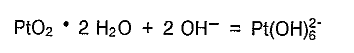
- Pd O or Pt O -forming activators can advantageously be added to the alkaline medium as precursors.
- the hydroxo compound is adsorbed on the surface, so that subsequent immersion in a reducing solution of, for example, SnCl2 / HCl or hypophosphite / NaOH or boranates, aminoboranes or hydrazine compounds, the metallic Pt or Pd Form germs.
- a direct activator addition of platinum or palladium metal colloids is also possible; the resulting colloid particles are then anchored in the micro-roughened surface of the ceramic body (substrate).
- copper it is advantageous to start from the respective precursor and add the hydroxide Cu (OH) 2 to the melt, which is readily soluble in NaOH and, for example, with the subsequent reduction treatment on the substrate surface depending on the intended application
- Glucose as a reducing agent to Cu2O (adhesion promoter) or with formaldehyde to Cu O (activator germ) can be reduced.
- Ag nuclei which are added to the Cu (OH) 2 as AgOH in a low concentration and reduced to Ag O , have an activity-increasing effect.
- the method according to the invention can also be applied to an acid pretreatment of certain types of ceramics, e.g. Barium titanate ceramics.
- the digestion medium KHSO4 or NH4HSO4 in the melt tin (II) sulfate can be added as a sensitizer, which is then reduced to Sn (OH) 2 in the subsequent hydrolysis.
- Hydrofluoric acid or fluoride-containing melts can advantageously be mixed with SnF2, which also forms Sn (OH) 2 after a hydrolysis process and is suitable as a sensitizer for Pd2+ or Ag+ reduction.
- silver nuclei can be reduced by reducing AgF, e.g. be generated directly on the substrate surface with formaldehyde.
- a high-purity Al2O3 ceramic (99.6% Al2O3) is immersed in a sodium hydroxide melt that contains 0.01 to 10 g / l, preferably 0.5 g / l, of sodium silicate contains, which is added as a stoichiometric amount of highly disperse silica (eg as Aerosil 200 from Degussa, Frankfurt) has been.
- the temperature of the melt is 350 ° C.
- the duration of the treatment is 1 to 10 minutes, preferably 6 minutes, depending on the degree of roughening desired.
- the ceramic part is then rinsed in water, activated in a known manner with SnCl2 / PdCl2, electrolessly copper-plated to a layer thickness of 0.5 ⁇ m, heated for 10 min at 450 ° C. in a nitrogen atmosphere and then further electrolessly or electrolytically copper-plated.
- the adhesive strength of a 10-15 ⁇ m thick copper layer in the vertical peel test is over 25 N / mm2 and thus exceeds the breaking strength of the ceramic.
- the Al2O3 ceramic parts are treated in the melt for 1 to 19 min, preferably 8 min, at 450 ° C, then briefly rinsed in water, immersed in a weakly hydrochloric acid PdCl2 solution with 0.5 g / l PdCl2 and then de-energized -chemically copper-plated.
- a treatment at 150 ° C. for 15 minutes is sufficient due to the increased surface roughening of the ceramic in order to give the subsequently applied copper coating a sufficiently high adhesion.
- a palladium colloid (palladium black) is finely distributed in the NaOH melt in a concentration of 1 g / l.
- the Pd entry into the melt is advantageously carried out in such a way that the palladium colloid is first mixed with molten sodium hydroxide in a small separate gold crucible and then added to the main part of the melt with stirring. After immersing the ceramic parts in the melt and briefly rinsing them in water, they can be chemically copper-plated directly and then thermally treated.
- Barium titanate ceramic substrates are pretreated in a melt of ammonium bisulfate, to which 10% by weight of stannous acetate has been added. The exposure time is around 10 min at a temperature of 200 ° C. After rinsing in water, the substrate surface is coated with Pd seeds by immersion in a hydrochloric acid solution of 0.5 g / l PdCl2 ⁇ 2 H2O. Then the parts are electrolessly chemically coppered and galvanically reinforced. The adhesion of the copper layer exceeds the breaking strength of the ceramic.
Landscapes
- Chemical & Material Sciences (AREA)
- Engineering & Computer Science (AREA)
- General Chemical & Material Sciences (AREA)
- Chemical Kinetics & Catalysis (AREA)
- Materials Engineering (AREA)
- Mechanical Engineering (AREA)
- Metallurgy (AREA)
- Organic Chemistry (AREA)
- Manufacturing & Machinery (AREA)
- Microelectronics & Electronic Packaging (AREA)
- Chemically Coating (AREA)
- Manufacturing Of Printed Wiring (AREA)
Description
- Die Erfindung betrifft ein Verfahren zur Metallisierung von Keramik nach Patentanspruch 1.
- Es ist bekannt, daß beispielsweise die in der Elektrotechnik und Elektronik häufig eingesetzte, hochreine Aluminiumoxid-Keramik zur Verbesserung der Benetzbarkeit und der Haftfestigkeit vorteilhaft in einer alkalischen Lösung oder Schmelze vorbehandelt wird. Dabei wird die Keramik oberflächlich aufgeschlossen, chemisch inerte Oberflächenbereiche werden abgetragen und eine chemisch aktive Oberfläche wird erzeugt. Außerdem erfolgt dabei eine mehr oder weniger starke Aufrauhung der Oberfläche, die mechanische Verankerungsmöglichkeiten zur Steigerung der Haftfestigkeit der Metallauflage bietet. Ist eine Aufrauhung aus elektrischen Gründen unerwünscht, so wird ein Haftvermittler eingesetzt, z.B. Cu₂O nach dem deutschen Patent DE-PS 25 33 524 oder Kieselsäure nach dem deutschen Patent DE-PS 20 04 133, der mit der Keramikoberfläche reagiert und gleichzeitig zur Kupferschicht Bindungen ausbildet. Es ist außerdem bekannt, die Keramikoberfläche durch Tauchen in Sensibilisierungs- und/oder Aktivierungslösungen mit beispielsweise Sn/Pd-Katalysatorkeimen zu belegen und anschließend mit einem handelsüblichen chemischen Kupferbad zu verkupfern. Die genannten Schritte stellen in der Regel Einzelschritte dar, die sukzessive durchgeführt werden. Ein derartiges Verfahren ist in nachteiliger Weise unwirtschaftlich, insbesondere bei einer industriellen Massenfertigung.
- Aus der EP-A-0 035 626 ist ein Metallisierungsverfahren bekannt, bei welchem die zu metallisierende Keramikoberfläche zunächst mit einer Alkalimetall-Silikat-Lösung beschichtet wird. Diese Lösung enthält ein Metallsalz, das, nach einer Reduktion, katalytisch wirkt auf das aus einem stromlos chemisch arbeitenden Metallisierungsbad abzuscheidende Metall. Nach dem Auftragen der Lösung wird der entstandene Lösungsfilm getrocknet, so daß eine Schicht entsteht. Diese Schicht wird anschließend bei erhöhter Temperatur, z.B. 200° C, eingebrannt. Anschließend kann die eingebrannte Schicht mit einer auf das Metallsalz reduzierend wirkenden Lösung behandelt werden. Danach erfolgt die stromlos chemische Metallisierung, z.B. mit Nickel oder Kobalt.
- Aus der EP-A-0 128 476 ist weiterhin ein Metallisierungsverfahren bekannt, bei welchem die zu metallisierende Keramikoberfläche zunächst in einer Alkalihydroxid-Schmelze, welche den Schmelzpunkt erniedrigende Zusätze enthalten kann, behandelt wird. Anschließend wird die angeätzte Oberfläche mit einer sauren Lösung, die Halogene enthält, behandelt. Diese Lösung wird an der angeätzten Oberfläche adsorbiert. Dann erfolgt eine Sensibilisierung, z.B. in einer sauren Zinnchlorid-Lösung, eine Aktivierung, z.B. in einer sauren Palladiumchlorid-Lösung, und die stromlos chemische Metallisierung, z.B. mit Kupfer.
- Der Erfindung liegt daher die Aufgabe zugrunde, ein derartiges Verfahren dahingehend zu verbessern, daß einzelne Verfahrensschritte zusammengefaßt werden, daß eine hohe Haftfestigkeit der aufgebrachten Metallschicht erreicht wird und daß eine kostengünstige sowie zuverlässige Herstellung ermöglicht wird, insbesondere bei einer industriellen Massenfertigung.
- Diese Aufgabe wird gelöst durch die im Patentanspruch 1 angegebenen Merkmale. Zweckmäßige Ausgestaltungen und/oder Weiterbildungen sind den Unteransprüchen entnehmbar.
- Die Erfindung wird im folgenden anhand von Ausführungsbeispielen näher erläutert.
- Bei einer beispielhaft gewählten Verkupferung einer Keramikoberfläche ist lediglich ein einziger Vorbehandlungsschritt erforderlich vor der eigentlichen Verkupferung. Einer dafür erforderlichen alkalischen oder sauren Vorbehandlungschmelze wird ein Haftvermittler (oder dessen Vorstufe) und/oder ein Sensibilisator (oder dessen Vorstufe) und/oder ein Aktivator im Sinne eines Katalysators (oder dessen Vorstufe) ugesetzt. Als Haftvermittler kommen insbesondere in Betracht Verbindungen der Elemente der III. bis VI. Hauptgruppe und/oder der I. bis VIII. Nebengruppe des Periodensystems, beispielsweise Silicate, Molybdate, Wolframate, Vanadate, Titanate, Stannate, Cuprate, Manganate und Ferrate in unterschiedlichen Oxidationsstufen. Die diesen Verbindungen zugrundeliegenden Oxide vermögen mit den Bestandteilen der Keramik insbesondere in der Hitze Alumosilicate, Spinelle, z.B. des Typs

oder andere Mischoxide zu bilden, auf denen der Haftmechanismus basiert. Dabei bedeuten MI bzw. MII bzw. MIII ein- bzw. zwei- bzw. dreiwertige Elemente der genannten Gruppen. - Als Sensibilisatorzusatz wird eine alkalische Stannat(II)-Lösung verwendet oder Zinn(II)-oxid oder -hydroxid der Alkalihydroxid-Schmelze zugesetzt. Da diese Medien starke Reduktionsmittel darstellen, vermögen sie die im weiteren Verfahrensgang angebotenen Pd²⁺-Ionen zu PdO-Keimen zu reduzieren, die ihrerseits bekanntlich die stromlos-chemische Kupferabscheidung katalysieren. Da Zinn(II)-haltige Medien andererseits durch Luftsauerstoff allmählich unwirksam werden, ist eine Anwendung dieser Medien unter Inertgas zweckmäßig.
- Alternativ dazu können PdO- oder PtO-bildende Aktivatoren dem alkalischen Medium als Vorstufen vorteilhaft zugesetzt werden. Geeignete Verbindungen sind beispielsweise wasserhaltige Palladium- oder Platinoxide, die in starken Alkalien, insbesondere in der Hitze, in die entsprechenden Hydroxokomplexe überführt werden, z.B. nach der Formel:
Beim Tauchen des Keramikkörpers in ein solches Vorbehandlungsmedium wird die Hydroxoverbindung auf der Oberfläche adsorbiert, so daß sich beim anschließenden Eintauchen in eine reduzierend wirkende Lösung von z.B. SnCl₂/HCl oder Hypophosphit/NaOH oder Boranaten, Aminoboranen oder Hydrazinverbindungen, die metallischen Pt- oder Pd-Keime bilden. Auch ein direkter Aktivatorzusatz von Platin- oder Palladiummetallkolloiden ist möglich; eine Verankerung der entstehenden Kolloidteilchen erfolgt dann in der mikroaufgerauhten Oberfläche des Keramikkörpers (Substrats). Will man Kupfer als Aktivator verwenden, so ist es vorteilhaft, von der jeweiligen Vorstufe auszugehen und der Schmelze das Hydroxid Cu(OH)₂ zuzusetzen, das in NaOH gut löslich ist und sich bei der anschließenden Reduktionsbehandlung auf der Substratoberfläche je nach angestrebtem Einsatzfall z.B. mit Glucose als Reduktionsmittel zu Cu₂O (Haftvermittler) oder mit Formaldehyd zu CuO (Aktivatorkeim) reduzieren läßt. In letzterem Falle wirken sich Ag-Keime, die als AgOH in geringer Konzentration dem Cu(OH)₂ zugefügt werden und zu AgO reduziert werden, aktivitätssteigernd aus. - Analog der Vorbehandlung von Keramik in alkalischem Medium kann das erfindungsgemäße Verfahren auch auf eine saure Vorbehandlung von bestimmten Keramiktypen, z.B. Bariumtitanat-Keramik, angewandt werden. Beispielsweise kann dem Aufschlußmedium KHSO₄ oder NH₄HSO₄ in der Schmelze Zinn(II)-sulfat als Sensibilisator zugesetzt werden, das dann bei der nachfolgenden Hydrolyse zu Sn(OH)₂ reduziert wird. Flußsaure oder fluoridhaltige Schmelzen können vorteilhaft mit SnF₂ versetzt werden, das nach einem Hydrolyseprozeß ebenfalls Sn(OH)₂ bildet und als Sensibilisator zur Pd²⁺- oder Ag⁺-Reduktion geeignet ist. Andererseits können Silberkeime auf entsprechendem Wege durch Reduktion von zugesetztem AgF z.B. mit Formaldehyd unmittelbar auf der Substratoberfläche erzeugt werden.
- Zur gleichzeitigen Vorbehandlung durch Oberflächenreinigung und Mikroaufrauhung sowie Beschichtung mit einem Haftvermittler wird eine hochreine Al₂O₃-Keramik (99,6 % Al₂O₃) in eine Natriumhydoxid-Schmelze getaucht, die 0,01 bis 10 g/l, vorzugsweise 0,5 g/l Natriumsilicat enthält, das als stöchiometrische Menge hochdisperser Kieselsäure (z.B. als Aerosil 200 der Fa. Degussa, Frankfurt) zugegeben wurde. Die Temperatur der Schmelze beträgt 350°C. Die Dauer der Behandlung beträgt je nach gewünschtem Aufrauhungsgrad 1 bis 10 min, vorzugsweise 6 min. Anschließend wird das Keramikteil in Wasser gespült, mit SnCl₂/PdCl₂ in bekannter Weise aktiviert, auf eine Schichtdicke von 0,5µm chemisch stromlos verkupfert, 10 min bei 450 °C in Stickstoffatmosphäre erhitzt und anschließend chemisch stromlos oder galvanisch weiterverkupfert. Die Haftfestigkeit einer 10-15 µm dicken Kupferschicht beträgt im senkrechten Abzugstest über 25 N/mm² und übersteigt damit die Bruchfestigkeit der Keramik.
- Verfahren gemäß Beispiel 1 mit dem Unterschied, daß der Natriumhydroxid-Schmelze anstelle von Kieselsäure 0,01 bis 10 g/l, vorzugsweise 0,3 g/l, frisch gefälltes Zinn(II)-hydroxid unter Stickstoffatmosphäre zugesetzt werden. Die Fällung wurde unmittelbar vorher durch Umsetzung von SnCl₂ in schwach salzsaurer Lösung mit NaOH-Lösung unter Stickstoffatmosphäre durchgeführt. Durch ein Rührwerk wird das Zinn(II)-hydroxid in der Schmelze fein verteilt bis es sich vollständig gelöst hat. Die Al₂O₃-Keramikteile werden in der Schmelze 1 bis 19 min, vorzugsweise 8 min, bei 450 °C behandelt, anschließend kurz in Wasser gespült, zur Aktivierung in eine schwach salzsaure PdCl₂-Lösung mit 0,5 g/l PdCl₂ getaucht und anschließend stromlos-chemisch verkupfert. Als thermische Nachbehandlung genügt infolge der stärkeren Oberflächenaufrauhung der Keramik eine Behandlung bei 150 °C für 15 min, um der nachfolgend aufgebrachten Kupferauflage eine ausreichend hohe Haftung zu verleihen.
- Verfahren gemäß Beispiel 2 mit dem Unterschied, daß anstelle von Zinn(II)-hydroxid Ag-aktiviertes Kupfer(II)-hydroxid in einer Konzentration von 0,01 bis 1o g/l, vorzugsweise 0,8 g/l, in der Schmelze eingesetzt wird. Dieses wurde vorher durch Fällung aus einer Kupfer(II)-nitratlösung mit verdünnter Natronlauge frisch hergestellt, wobei der Kupfer(II)-nitratlösung etwas Silbernitrat (im Gewichtsverhältnis Cu : Ag wie 100 : 1) zugefügt worden war. Nach dem Eintauchen der Keramikteile in die Schmelze werden diese in einer Lösung von 2 g/l SnCl₂, 10 g/l 35 %igem Formaldehyd und Natronlauge bis pH = 10 etwa 1 min lang vorgespült und anschließend mit Wasser klargespült. Die darauffolgende Verkupferung erfolgt wie in Beispiel 2.
- Verfahren gemäß Beispiel 1 mit dem Unterschied, daß zusätzlich zur Kieselsäure in der NaOH-Schmelze ein Palladiumkolloid (Palladiummohr) in einer Konzentration von 1 g/l feinst verteilt wird. Der Pd-Eintrag in die Schmelze erfolgt dabei zweckmäßigerweise in der Form, daß das Palladiumkolloid zunächst in einem kleinen separaten Goldtiegel mit geschmolzenem Natriumhydroxid vermischt und dann erst dem Hauptteil der Schmelze unter Rühren zugesetzt wird. Nach dem Eintauchen der Keramikteile in die Schmelze und kurzem Zwischenspülen in Wasser können diese direkt chemisch verkupfert und anschließend thermisch nachbehandelt werden.
- Bariumtitanat-Keramiksubstrate werden in einer Schmelze aus Ammoniumhydrogensulfat vorbehandelt, der 10 Gew.-% Zinn(II)-acetat zugesetzt wurden. Die Einwirkdauer beträgt bei einer Temperatur von 200 °C etwa 10 min. Nach Spülen in Wasser erfolgt die Belegung der Substratoberfläche mit Pd-Keimen durch Tauchen in eine salzsaure Lösung von 0,5 g/l PdCl₂ · 2 H₂O. Anschließend werden die Teile stromlos-chemisch verkupfert und galvanisch verstärkt. Die Haftung der Kupferauflage übertrifft die Bruchfestigkeit der Keramik.
Claims (11)
- Verfahren zur Metallisierung von Keramik, insbesondere zu deren naßchemischen Verkupferung, bei dem in einem einzigen Vorbehandlungsschnitt gleichzeitig:a) die Reinigung und die Aufrauhung der Keramikoberfläche durchgeführt wird, undb) eine chemische Aktivierung der Keramikoberfläche erfolgt und deren Belegung mit einem Haftvermittler und/oder Sensibilisator und/oder Aktivator und/oder Katalysator oder deren Vorstufen für eine nachfolgende, chemische Metallisierung, wobei die Oberfläche der Keramik in einer die Oberfläche anätzenden Schmelze, welche Substanzen, die durch Belegung der Keramikoberfläche als Haftvermittler und/oder Sensibilisator und/oder Aktivator und/oder Katalysator oder deren Vorstufen wirken, enthält und welche eine gegenüber der Raumtemperatur erhöhte Temperatur besitzt, aufgeschlossen wird und bei dem nach der Behandlung mit der Schmelze die Oberfläche gespült wird und anschließend die Metallisierung durchgeführt wird.
- Verfahren nach Anspruch 1, dadurch gekennzeichnet, daß die Schmelze eine Temperatur in einem Temperaturbereich von 100 bis 1000°C besitzt.
- Verfahren nach Anspruch 1 oder 2, dadurch gekennzeichnet, daß bei einer alkalisch angreifbaren Keramik eine alkalische Schmelze, die mindestens ein Alkalihydroxid enthält und deren Temperatur in einem Temperaturbereich von 150 bis 600°C liegt, erwendet wird.
- Verfahren nach einem der vorhergehenden Ansprüche, dadurch gekennzeichnet daß bei einer durch Säure angreifbaren Keramik eine saure Schmelze, die Ammoniumhydrogensulfat enthält und eine Temperatur in einem Temperaturbereich von 100 bis 1200°C besitzt, verwendet wird.
- Verfahren nach einem der vorhergehenden Ansprüche, dadurch gekennzeichnet, daß das Vorbehandlungsmedium ein Silicat, Molybdat, Wolframat, Vanadat, Titanat, Manganat, Ferrat, Cuprat, Stannat oder ein Gemisch davon enthält.
- Verfahren nach einem der vorhergehenden Ansprüche, dadurch gekennzeichnet, daß das Vorbehandlungsmedium einen Sensibilisator oder dessen Vorstufe enthält.
- Verfahren nach einem der vorhergehenden Ansprüche, dadurch gekennzeichnet, daß als Sensibilisator eine Zinn(II)-Verbindung gewählt wird.
- Verfahren nach einem der vorhergehenden Ansprüche, dadurch gekennzeichnet, daß das Vorbehandlungsmedium einen Aktivator bzw. Katalysator oder dessen Vorstufe, für die chemische Metallisierung enthält.
- Verfahren nach einem der vorhergehenden Ansprüche, dadurch gekennzeichnet, daß als Aktivator bzw. Katalysator oder dessen Vorstufe, eine Verbindung der Elemente Ni, Cu, Ag, Au, Pd, Pt oder eines dieser Elemente selbst in feiner, kolloider Verteilung verwendet wird.
- Verfahren nach einem der vorhergehenden Ansprüche. dadurch gekennzeichnet, daß als Haftvermittler Kupferoxid oder Kieselsäure oder ein Alkalisilicat verwendet wird.
- Verfahren nach einem der vorhergehenden Ansprüche, dadurch gekennzeichnet, daß Cu₂ O als Kupferoxid verwendet wird.
Priority Applications (1)
| Application Number | Priority Date | Filing Date | Title |
|---|---|---|---|
| AT86108643T ATE66967T1 (de) | 1985-07-04 | 1986-06-25 | Verfahren zur metallisierung von keramik. |
Applications Claiming Priority (2)
| Application Number | Priority Date | Filing Date | Title |
|---|---|---|---|
| DE3523957 | 1985-07-04 | ||
| DE19853523957 DE3523957A1 (de) | 1985-07-04 | 1985-07-04 | Verfahren zur metallisierung von keramik |
Publications (2)
| Publication Number | Publication Date |
|---|---|
| EP0210436A1 EP0210436A1 (de) | 1987-02-04 |
| EP0210436B1 true EP0210436B1 (de) | 1991-09-04 |
Family
ID=6274971
Family Applications (1)
| Application Number | Title | Priority Date | Filing Date |
|---|---|---|---|
| EP19860108643 Expired - Lifetime EP0210436B1 (de) | 1985-07-04 | 1986-06-25 | Verfahren zur Metallisierung von Keramik |
Country Status (5)
| Country | Link |
|---|---|
| US (1) | US4812202A (de) |
| EP (1) | EP0210436B1 (de) |
| JP (1) | JPS627687A (de) |
| AT (1) | ATE66967T1 (de) |
| DE (2) | DE3523957A1 (de) |
Families Citing this family (10)
| Publication number | Priority date | Publication date | Assignee | Title |
|---|---|---|---|---|
| US5069591A (en) * | 1988-03-24 | 1991-12-03 | Tel Sagami Limited | Semiconductor wafer-processing apparatus |
| US5871810A (en) * | 1995-06-05 | 1999-02-16 | International Business Machines Corporation | Plating on nonmetallic disks |
| DE10054544A1 (de) * | 2000-11-01 | 2002-05-08 | Atotech Deutschland Gmbh | Verfahren zum chemischen Metallisieren von Oberflächen |
| DE10208120A1 (de) * | 2002-02-26 | 2003-09-18 | Schloetter Fa Dr Ing Max | Verfahren zur Metallisierung von Keramik auf Basis von Titanaten |
| JP2005022956A (ja) * | 2003-07-02 | 2005-01-27 | Rohm & Haas Electronic Materials Llc | セラミックの金属化 |
| DE102004030800B4 (de) * | 2004-06-25 | 2017-05-18 | Epcos Ag | Verfahren zur Herstellung einer keramischen Leiterplatte |
| US20090238979A1 (en) * | 2008-03-21 | 2009-09-24 | William Decesare | Method of Applying Catalytic Solution for Use in Electroless Deposition |
| JP5750721B2 (ja) * | 2010-08-12 | 2015-07-22 | Dowaエレクトロニクス株式会社 | 銀粉およびその製造方法、導電ペースト並びに電子部品 |
| GB2486202A (en) * | 2010-12-06 | 2012-06-13 | Cambridge Display Tech Ltd | Adhesion layer for solution-processed transition metal oxides on inert metal contacts of organic thin film transistors. |
| CN118834089B (zh) * | 2024-08-08 | 2025-03-14 | 江苏富乐华半导体科技股份有限公司 | 一种制备氮化铝覆铜陶瓷载板的dcb生产方法 |
Family Cites Families (7)
| Publication number | Priority date | Publication date | Assignee | Title |
|---|---|---|---|---|
| US3607473A (en) * | 1968-03-04 | 1971-09-21 | Macdermid Inc | Compositions for and method of pretreating plastic surfaces to improve adhesion of coating materials |
| US3770528A (en) * | 1971-09-29 | 1973-11-06 | Martin Processing Co Inc | Method for the surface treatment of polyimide materials |
| US4259409A (en) * | 1980-03-06 | 1981-03-31 | Ses, Incorporated | Electroless plating process for glass or ceramic bodies and product |
| US4428986A (en) * | 1982-11-18 | 1984-01-31 | Eaton Corporation | Method of preparing a beryllia substrate for subsequent autocatalytic deposition of a metallized film directly thereon |
| US4604299A (en) * | 1983-06-09 | 1986-08-05 | Kollmorgen Technologies Corporation | Metallization of ceramics |
| US4647477A (en) * | 1984-12-07 | 1987-03-03 | Kollmorgen Technologies Corporation | Surface preparation of ceramic substrates for metallization |
| DE3523961A1 (de) * | 1985-07-04 | 1987-01-15 | Licentia Gmbh | Vorrichtung zum behandeln mindestens eines keramikgegenstandes in einer alkalihydroxidschmelze |
-
1985
- 1985-07-04 DE DE19853523957 patent/DE3523957A1/de not_active Withdrawn
-
1986
- 1986-06-25 AT AT86108643T patent/ATE66967T1/de not_active IP Right Cessation
- 1986-06-25 EP EP19860108643 patent/EP0210436B1/de not_active Expired - Lifetime
- 1986-06-25 DE DE8686108643T patent/DE3681221D1/de not_active Expired - Fee Related
- 1986-07-02 JP JP61154296A patent/JPS627687A/ja active Granted
- 1986-07-07 US US06/885,254 patent/US4812202A/en not_active Expired - Fee Related
Also Published As
| Publication number | Publication date |
|---|---|
| EP0210436A1 (de) | 1987-02-04 |
| DE3681221D1 (de) | 1991-10-10 |
| DE3523957A1 (de) | 1987-01-08 |
| ATE66967T1 (de) | 1991-09-15 |
| JPS627687A (ja) | 1987-01-14 |
| JPH0223512B2 (de) | 1990-05-24 |
| US4812202A (en) | 1989-03-14 |
Similar Documents
| Publication | Publication Date | Title |
|---|---|---|
| DE3543613C2 (de) | ||
| US4622069A (en) | Catalyst composition for forming electroless plating on ceramics | |
| US3993799A (en) | Electroless plating process employing non-noble metal hydrous oxide catalyst | |
| DE69830287T2 (de) | Stromloses Plattierverfahren | |
| EP0210437B1 (de) | Verfahren zur chemischen Metallisierung eines elektrisch schlecht leitenden Trägerkörpers aus einem anorganischen Material | |
| EP0290539B1 (de) | Verfahren zur chemischen behandlung von keramikkörpern mit nachfolgender metallisierung | |
| EP0210436B1 (de) | Verfahren zur Metallisierung von Keramik | |
| DE10054544A1 (de) | Verfahren zum chemischen Metallisieren von Oberflächen | |
| DE2533524C3 (de) | Verfahren zur Herstellung eines Belages aus Kupfer oder einer Kupferlegierung auf einem Trägerkörper | |
| EP2639333A1 (de) | Verfahren zum Metallisieren nichtleitender Kunststoffoberflächen | |
| US4181760A (en) | Method for rendering non-platable surfaces platable | |
| DE4119807C1 (en) | Bath for electroless plating of e.g. nickel@, zinc@ - consisting of e.g. titanium halogenide(s), cyclo:pentadienyl-complex cpds. of titanium sulphate and hydroxide | |
| CH629853A5 (de) | Verfahren zum stromlosen metallisieren. | |
| EP0142691B1 (de) | Verfahren zur Aktivierung von Substraten für die stromlose Metallisierung | |
| DE69204564T2 (de) | Verfahren zur selektiven stromlosen Metallisierung eines Musters aus einem anderen Werkstoff als Glas auf einem Glasträger. | |
| US4082557A (en) | Silver base activating solutions for electroless copper deposition | |
| US4321285A (en) | Electroless plating | |
| US4820547A (en) | Activators for colloidal catalysts in electroless plating processes | |
| DE2004133A1 (de) | Verfahren zur Metallisierung von glaesernen oder keramischen Traegerkoerpern | |
| EP1478607B1 (de) | Verfahren zur metallisierung von keramik auf basis von titanaten | |
| DE3814224C1 (en) | Process for pretreating aluminium nitride ceramic to be metallised | |
| DE1814055C3 (de) | Verfahren zur Vorbehandlung von isolierenden Tragern vor der stromlosen Metallabscheidung | |
| US4305997A (en) | Electrolessly metallized product of non-catalytic metal or alloy | |
| DE2046708A1 (de) | Voraetzung von Acrylnitril Butadien Styrol Harzen fur die stromlose Metallab scheidung | |
| WO1995027813A1 (de) | Palladiumkolloid-lösung und deren verwendung |
Legal Events
| Date | Code | Title | Description |
|---|---|---|---|
| PUAI | Public reference made under article 153(3) epc to a published international application that has entered the european phase |
Free format text: ORIGINAL CODE: 0009012 |
|
| AK | Designated contracting states |
Kind code of ref document: A1 Designated state(s): AT BE CH DE FR GB IT LI LU NL SE |
|
| 17P | Request for examination filed |
Effective date: 19870709 |
|
| 17Q | First examination report despatched |
Effective date: 19881130 |
|
| 17Q | First examination report despatched |
Effective date: 19900808 |
|
| GRAA | (expected) grant |
Free format text: ORIGINAL CODE: 0009210 |
|
| AK | Designated contracting states |
Kind code of ref document: B1 Designated state(s): AT BE CH DE FR GB IT LI LU NL SE |
|
| REF | Corresponds to: |
Ref document number: 66967 Country of ref document: AT Date of ref document: 19910915 Kind code of ref document: T |
|
| ITF | It: translation for a ep patent filed | ||
| REF | Corresponds to: |
Ref document number: 3681221 Country of ref document: DE Date of ref document: 19911010 |
|
| ET | Fr: translation filed | ||
| GBT | Gb: translation of ep patent filed (gb section 77(6)(a)/1977) | ||
| PG25 | Lapsed in a contracting state [announced via postgrant information from national office to epo] |
Ref country code: GB Effective date: 19920625 Ref country code: AT Effective date: 19920625 |
|
| PG25 | Lapsed in a contracting state [announced via postgrant information from national office to epo] |
Ref country code: SE Effective date: 19920626 |
|
| PG25 | Lapsed in a contracting state [announced via postgrant information from national office to epo] |
Ref country code: LU Free format text: LAPSE BECAUSE OF NON-PAYMENT OF DUE FEES Effective date: 19920630 Ref country code: LI Effective date: 19920630 Ref country code: CH Effective date: 19920630 Ref country code: BE Effective date: 19920630 |
|
| PLBE | No opposition filed within time limit |
Free format text: ORIGINAL CODE: 0009261 |
|
| STAA | Information on the status of an ep patent application or granted ep patent |
Free format text: STATUS: NO OPPOSITION FILED WITHIN TIME LIMIT |
|
| 26N | No opposition filed | ||
| BERE | Be: lapsed |
Owner name: LICENTIA PATENT-VERWALTUNGS-G.M.B.H. Effective date: 19920630 |
|
| PG25 | Lapsed in a contracting state [announced via postgrant information from national office to epo] |
Ref country code: NL Effective date: 19930101 |
|
| NLV4 | Nl: lapsed or anulled due to non-payment of the annual fee | ||
| GBPC | Gb: european patent ceased through non-payment of renewal fee |
Effective date: 19920625 |
|
| PG25 | Lapsed in a contracting state [announced via postgrant information from national office to epo] |
Ref country code: FR Effective date: 19930226 |
|
| REG | Reference to a national code |
Ref country code: CH Ref legal event code: PL |
|
| PG25 | Lapsed in a contracting state [announced via postgrant information from national office to epo] |
Ref country code: DE Effective date: 19930302 |
|
| REG | Reference to a national code |
Ref country code: FR Ref legal event code: ST |
|
| EUG | Se: european patent has lapsed |
Ref document number: 86108643.7 Effective date: 19930109 |
|
| PG25 | Lapsed in a contracting state [announced via postgrant information from national office to epo] |
Ref country code: IT Free format text: LAPSE BECAUSE OF NON-PAYMENT OF DUE FEES;WARNING: LAPSES OF ITALIAN PATENTS WITH EFFECTIVE DATE BEFORE 2007 MAY HAVE OCCURRED AT ANY TIME BEFORE 2007. THE CORRECT EFFECTIVE DATE MAY BE DIFFERENT FROM THE ONE RECORDED. Effective date: 20050625 |