EP0209152B1 - Pre-exposure method for increased sensitivity in high contrast resist development - Google Patents
Pre-exposure method for increased sensitivity in high contrast resist development Download PDFInfo
- Publication number
- EP0209152B1 EP0209152B1 EP86109897A EP86109897A EP0209152B1 EP 0209152 B1 EP0209152 B1 EP 0209152B1 EP 86109897 A EP86109897 A EP 86109897A EP 86109897 A EP86109897 A EP 86109897A EP 0209152 B1 EP0209152 B1 EP 0209152B1
- Authority
- EP
- European Patent Office
- Prior art keywords
- photoresist
- radiation
- pattern
- exposure
- positive
- Prior art date
- Legal status (The legal status is an assumption and is not a legal conclusion. Google has not performed a legal analysis and makes no representation as to the accuracy of the status listed.)
- Expired - Lifetime
Links
Images
Classifications
-
- G—PHYSICS
- G03—PHOTOGRAPHY; CINEMATOGRAPHY; ANALOGOUS TECHNIQUES USING WAVES OTHER THAN OPTICAL WAVES; ELECTROGRAPHY; HOLOGRAPHY
- G03C—PHOTOSENSITIVE MATERIALS FOR PHOTOGRAPHIC PURPOSES; PHOTOGRAPHIC PROCESSES, e.g. CINE, X-RAY, COLOUR, STEREO-PHOTOGRAPHIC PROCESSES; AUXILIARY PROCESSES IN PHOTOGRAPHY
- G03C5/00—Photographic processes or agents therefor; Regeneration of such processing agents
- G03C5/18—Diazo-type processes, e.g. thermal development, or agents therefor
-
- G—PHYSICS
- G03—PHOTOGRAPHY; CINEMATOGRAPHY; ANALOGOUS TECHNIQUES USING WAVES OTHER THAN OPTICAL WAVES; ELECTROGRAPHY; HOLOGRAPHY
- G03F—PHOTOMECHANICAL PRODUCTION OF TEXTURED OR PATTERNED SURFACES, e.g. FOR PRINTING, FOR PROCESSING OF SEMICONDUCTOR DEVICES; MATERIALS THEREFOR; ORIGINALS THEREFOR; APPARATUS SPECIALLY ADAPTED THEREFOR
- G03F7/00—Photomechanical, e.g. photolithographic, production of textured or patterned surfaces, e.g. printing surfaces; Materials therefor, e.g. comprising photoresists; Apparatus specially adapted therefor
- G03F7/20—Exposure; Apparatus therefor
- G03F7/2022—Multi-step exposure, e.g. hybrid; backside exposure; blanket exposure, e.g. for image reversal; edge exposure, e.g. for edge bead removal; corrective exposure
-
- G—PHYSICS
- G03—PHOTOGRAPHY; CINEMATOGRAPHY; ANALOGOUS TECHNIQUES USING WAVES OTHER THAN OPTICAL WAVES; ELECTROGRAPHY; HOLOGRAPHY
- G03F—PHOTOMECHANICAL PRODUCTION OF TEXTURED OR PATTERNED SURFACES, e.g. FOR PRINTING, FOR PROCESSING OF SEMICONDUCTOR DEVICES; MATERIALS THEREFOR; ORIGINALS THEREFOR; APPARATUS SPECIALLY ADAPTED THEREFOR
- G03F7/00—Photomechanical, e.g. photolithographic, production of textured or patterned surfaces, e.g. printing surfaces; Materials therefor, e.g. comprising photoresists; Apparatus specially adapted therefor
- G03F7/26—Processing photosensitive materials; Apparatus therefor
Definitions
- This invention relates to a developing process for high contrast resists and more particularly to the use of a high contrast resist developer after there has been a pre-exposure of the resist to UV-visible radiation, to produce increased sensitivity during lithographic processing of positive resist layers.
- sensitivity increases employing the method of the invention are 2-4 times higher.
- the photoresist and developer combination * provided the additional benefit of low film loss from unexposed resist.
- An illustrative photoresist system being, for example, a novolac type photoresist, available commercially as ACCULITHTM P-6010 with a potassium hydroxide type developer, available as Developer D-360, from Allied Corporation.
- This invention is applicable to lithographic exposures utilizing electrons, photons (eg. UV-visible, x-rays, etc.). Specifically, as a result of the increased sensitivity, higher throughput during lithographic processing for the fabrication of photomasks and semiconductor devices is realized.
- electrons, photons eg. UV-visible, x-rays, etc.
- Pattern definition for the production of semiconductor devices and photomasks is accomplished through the use of materials called resists.
- Resists which are typically organic polymers undergo a change in solubility response to a developer solution upon exposure to an irradiation source such as UV-visible light, x-rays or a beam of charged particles.
- an irradiation source such as UV-visible light, x-rays or a beam of charged particles.
- the resist is referred to as positive acting.
- a resin a photosensitive compound (sensitizer) and the solvent system. It is the role of the sensitizer to provide the resist its ability to withstand dissolution in the developer system. However, upon exposure to an irradiation source, the sensitizer is chemically transformed to a developer-soluble material. The net effect is that the dissolution rate of the exposed areas is greatly increased. However, the difference in dissolution rates between exposed and unexposed domains of the resist is only relative i.e. the unexposed resist may dissolve to some extent in the developer. For practical working resists, the differential solubility should be a factor of about 30 or greater i.e. film loss from unexposed resist should be less than 3%.
- the change in the differential solubility is not, however, a continuously linear function of exposure dose. Rather, at low exposures the dissolution rates between exposed and unexposed areas of a resist are not too dissimilar. As the dose is increased, a threshold value is reached where the dissolution rate increases sharply. Optimum exposure corresponds to the minimum dose which allows complete removal of exposed resist for a predetermined set of processing conditions. To quantify differences among resists, the term sensitivity may be defined as the minimum radiation dose which produces the desired ratio for the rate of dissolution between exposed and unexposed portions of the resist for a given set of parameters.
- a method which improves the sensitivity of positive resists for lithographic processing.
- the method utilizes initial pro-exposure of the resist to UV and/or visible light and subsequent development with a high contrast developer after lithographic exposure to form the desired image.
- film loss is negligible; enhancements in sensitivities were estimated for lithographies employing UV/visible and electrons as the irradiation source.
- Subject matter of the present invention is a process for developing a positive photoresist pattern according to claim 1. Embodiments of this process are subject matter of claims 2 to 7.
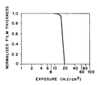
- the curve shown in the drawing illustrates the relationship between normalized film thickness of exposed resist as a function of UV/visible exposure dose for a given photoresist and developer system.
- a method that improves the sensitivity of resists to lithographic processing. Specifically, this improvement is derived from pre-exposure of the resist to UV and/or visible radiation from an appropriate source and development of the desired image using a high contrast developer.
- a significant feature of this invention is that film loss is reduced to a negligible value for unexposed resist.
- the resist must be photoactive to UV and/or visible radiation, i.e., an increase in solubility response must occur upon exposure. This requirement is characteristic of all known commercial positive photoresists although the feasibility as an electron beam resist for a given photoresist must be evaluated in the light of the task at hand. Additionally, the onset of this solubility response should be negligible at low exposure doses, desirably at zero, and should increase sharply at some threshold value. Of equal importance are the properties of the developer since it in combination with the resist, determines the sensitivity and contrast of the system.
- sensitizers of the diazo ketone type where the diazo and keto groups are at adjacent positions on the molecule have been found suitable for this invention.
- these sensitizers are quinone-diazide sulfonic acid derivatives as described, for example, in U.S. Patent Nos. 2,958,599; 3,046,110; 3,046,114; 3,046,116; 3,046,118; 3,046,119; 3,046,121; 3,046,122; 3,046,123; 3,106,465; 3,148,983; 3,635,709; 3,711,285; and 4,174,222 which the disclosed sensitizers are incorporated by reference in the present system.
- the developer of which potassium hydroxide, sodium hydroxide and sodium silicate are typical, must be capable of providing high contrast.
- aqueous alkali metal base such as those used in positive photoresist containing an alkali-soluble resin
- this is usually accomplished by the addition of a carboxylated surfactant to the developer as described in U.S. Patent Application Serial No. 660,600 filed on October 15, 1984 (P.D. 30-1834).
- contrast values of 3-7 are possible without the attendant film loss found in other systems.
- the resist may be applied to the substrate in the conventional manner as known by one skilled in the art. In most situations, this is accomplished by spin-coating to a desired thickness although other methods of application may be employed. Subsequent processing steps are generally identical to those used in the normal preparation of the coated substrate prior to lithographic exposure.
- Pre-exposure which immediately precedes lithographic exposure constitutes flooding of the coated substrate with UV and/or visible radiation from an appropriate source.
- the irradiation source should be capable of providing a stable and uniform illumination over the entire substrate surface. Additionally, it is desirable that the source be of sufficient intensity to minimize exposure time for a given radiation dose; hence, increasing throughput.
- Mercury arc lamps as found in most optical lithographic machines, are quite adequate for this purpose. Although a tungsten filament incandescent lamp may also be used, it is less desirable than the mercury arc lamp due to a lower efficiency in the production of UV radiation.
- Optimum pre-exposure dose will be dictated by the particular resist/developer combination to be used since the optical absorption characteristics and solubility responses will vary among different systems. Moreover, developing conditions (e.g. time and temperature) are additional factors to be considered in the selection of the irradiation dose. For one skilled in the art of lithographic processing, the determination of optimum pre-exposure dose of the film short of significant film loss for a given set of conditions is a relatively routine task.
- Film loss for a particular exposure dose is easily calculated by multiplying the original film thickness times the normalized film thickness. It is evident from the graph of the drawing that in order to completely remove the resist under the above conditions, a total exposure dose of 20 mJ/cm2 is necessary. Exposures up to ca. 10 mJ/cm2 result in no dissolution of the original film, i.e. zero film loss. The optimum pre-exposure dose would correspond to the maximum exposure before the film is solubilized by the exposure, i.e., before any significant film loss is encountered. The pre-exposure should not result in more than about 3-5 percent film loss and preferably substantially zero film loss. Therefore, lithographic exposure would be decreased by the amount equivalent to the pre-exposure dose for optical lithography.
- the resist/developer system used in the examples described below is AccuLithTM P-6010 photoresist which is a positive acting diazo ketone/novolac resin photoresist and AccuLithTM D-360 developer which is a KOH based developer. This system was chosen due to its high contrast which results in zero film loss under optimum processing conditions.
- the resist was applied to clean silicon wafer by spin-coating so as to produce a 1 micrometer thick film.
- the wafers were exposed to hexamethyldisilazane vapors for 10 minutes in a closed container prior to coating.
- the coated wafers were subsequently heated in a forced air convection oven for 30 minutes at 90°C to drive off residual solvents.
- the pre-exposure was effected by the illumination of the coated wafer surface with radiation from a mercury arc lamp for a preset duration corresponding to a known dose. This pre-exposure dose was measured by means of a UV light intensity meter manufactured by Optical Associates Incorporated. Lithographic exposure, both optical and electron beam, immediately followed. Development of the lithographic pattern was performed at 22°C for a desired length of time using the static immersion method. Film loss from unexposed resist was measured by interferometry.
- a coated substrate was prepared as described by the above procedure.
- the wafer was exposed to UV radiation through an Opto-Line step tablet resolution mask with windows of various exposure levels on the same wafer.
- a minimum exposure dose of 20 mJ/cm2 was required to completely develop the resist at 22°C and 1 minute development time.
- Film loss was determined to be zero with a contrast value (gamma) of 6.
- Example I The experiment of Example I was repeated but with pre-exposure included in the processing sequence. Prior to lithographic exposure, the coated wafer was flood exposed to 10 mJ/cm2 of UV/visible radiation as described above. Complete dissolution of the exposed resist required 10 mJ/cm2 of lithographic exposure with zero film loss and a gamma of 3.
- Electron beam exposure was performed with an unmodified Perkin-Elmer Autoscan microscope under manual control. An acceleration voltage of 20 KeV was employed at a beam current of 6nA.
- the raster pattern of the electron beam was roughly that of a square with a length of ca. 20 micrometers on each side at a magnification of 3000X and a working distance of 12mm; however, exposure across the rastered area was nonuniform. Relative changes in sensitivity were evaluated by comparison of the minimum exposure times required to completely clean the electron beam generated pattern.
- a coated wafer was prepared and exposed to the electron beam for 60 seconds. After a 60 second development in D-360, an underdeveloped pattern was generated as viewed through a scanning electron microscope. No film loss resulted from the unexposed resist.
- Example III The experiment described in Example III was repeated with the inclusion of pre-exposure. Immediately before electron beam processing, the coated wafer was flood exposed to a dose of 8.2 mJ/cm2 from a mercury arc lamp. A pattern similar to that produced in Example III was obtained after less than 30 seconds of electron beam exposure. No measurable film loss was observed illustrating the beneficial effect of the preexposure.
- Example III The experiment described in III was repeated but with the pre-exposure dose increased to 12.5 mJ/cm2. A pattern similar to that obtained in Example III resulted after exposure to the electron beam for 15 seconds. Film loss was ca. 1%. This run again illustrates the beneficial effect of pre-exposing the photosensitive film prior to the normal exposure.
- the invention may be applied in conjunction with various exposure systems known in the art, including exposure to electrons, photons, e.g., UV-visible radiation, ionic particles, i.e., atomic or molecular charged particles, and the like.
- exposure to electrons, photons e.g., UV-visible radiation
- ionic particles i.e., atomic or molecular charged particles, and the like.
Description
- This invention relates to a developing process for high contrast resists and more particularly to the use of a high contrast resist developer after there has been a pre-exposure of the resist to UV-visible radiation, to produce increased sensitivity during lithographic processing of positive resist layers. In comparison to resist layers which have not been subjected to the method of the present invention, sensitivity increases, employing the method of the invention are 2-4 times higher. Moreover, when used with a commercial photoresist system, the photoresist and developer combination* provided the additional benefit of low film loss from unexposed resist.
* An illustrative photoresist system being, for example, a novolac type photoresist, available commercially as ACCULITH™ P-6010 with a potassium hydroxide type developer, available as Developer D-360, from Allied Corporation. - This invention is applicable to lithographic exposures utilizing electrons, photons (eg. UV-visible, x-rays, etc.). Specifically, as a result of the increased sensitivity, higher throughput during lithographic processing for the fabrication of photomasks and semiconductor devices is realized.
- Pattern definition for the production of semiconductor devices and photomasks is accomplished through the use of materials called resists. Resists which are typically organic polymers undergo a change in solubility response to a developer solution upon exposure to an irradiation source such as UV-visible light, x-rays or a beam of charged particles. By definition, if the exposed areas attain a higher dissolution rate relative to the unexposed areas, the resist is referred to as positive acting.
- Most positive resists are produced from the combination of three basic ingredients: a resin, a photosensitive compound (sensitizer) and the solvent system. It is the role of the sensitizer to provide the resist its ability to withstand dissolution in the developer system. However, upon exposure to an irradiation source, the sensitizer is chemically transformed to a developer-soluble material. The net effect is that the dissolution rate of the exposed areas is greatly increased. However, the difference in dissolution rates between exposed and unexposed domains of the resist is only relative i.e. the unexposed resist may dissolve to some extent in the developer. For practical working resists, the differential solubility should be a factor of about 30 or greater i.e. film loss from unexposed resist should be less than 3%. The change in the differential solubility is not, however, a continuously linear function of exposure dose. Rather, at low exposures the dissolution rates between exposed and unexposed areas of a resist are not too dissimilar. As the dose is increased, a threshold value is reached where the dissolution rate increases sharply. Optimum exposure corresponds to the minimum dose which allows complete removal of exposed resist for a predetermined set of processing conditions. To quantify differences among resists, the term sensitivity may be defined as the minimum radiation dose which produces the desired ratio for the rate of dissolution between exposed and unexposed portions of the resist for a given set of parameters.
- In the fabrication of semiconductor devices and photomasks, it is advantageous to use a resist of highest sensitivity (minimum exposure time) in order to maximize throughput. This premise applies to any lithographic procedure irrespective of the irradiation source but is particularly important for direct write operations utilizing charged particles (e.g. electrons and ions). Currently, the chief impediment to the employment of these techniques as routine processing operations is their limited throughput. This limitation is especially severe for electron beam lithography which is cost prohibitive compared to the more commonly used UV-visible photolithography. Exceptions are those special applications which require geometries not attainable by the optical techniques. Moreover, it is anticipated that future need for smaller geometries will not be within the capabilities of photolithography to faithfully print the required details. Hence, electron and ion beam lithography are attractive alternatives to meet future needs. This realization has stimulated much research into these lithographic methods with particular emphasis on improving the sensitivity of existing resists and/or development of new resist systems.
- Accordingly, a need is present for a method which would obviate the disadvantage of low throughput due to limited sensitivity. Attempts to improve the sensitivity of photoresists have focused on the development of novel systems of, for example US-A-4250242, US-A-4298803 and US-A-4496647). Pre-exposure of a commercial photoresist with monochromatic light from an argon laser is reported for the recording of holograms as described by Beesley and Castledine, Applied Optics, vol. 9, 1970, pp. 2720-2724. However, values relating to film loss from unexposed resists are not known to have been considered in that reported study. In any event, it has not been known prior to any discovery that pre-exposure may be usefully applied to electron beam or optical developing techniques in the manner and for the particular purpose presented by this invention.
- In accordance with the invention, a method is described which improves the sensitivity of positive resists for lithographic processing. The method utilizes initial pro-exposure of the resist to UV and/or visible light and subsequent development with a high contrast developer after lithographic exposure to form the desired image. We have discovered that by employing the combination of resist/developer and pre-exposure dose controlled in the manner of the invention, film loss is negligible; enhancements in sensitivities were estimated for lithographies employing UV/visible and electrons as the irradiation source.
- Subject matter of the present invention is a process for developing a positive photoresist pattern according to
claim 1. Embodiments of this process are subject matter ofclaims 2 to 7. - The curve shown in the drawing illustrates the relationship between normalized film thickness of exposed resist as a function of UV/visible exposure dose for a given photoresist and developer system.
- In accordance with the invention, a method is described that improves the sensitivity of resists to lithographic processing. Specifically, this improvement is derived from pre-exposure of the resist to UV and/or visible radiation from an appropriate source and development of the desired image using a high contrast developer. A significant feature of this invention is that film loss is reduced to a negligible value for unexposed resist.
- In the practice of the invention, we have discovered that optimum results are obtained only after certain requisites are met. The resist must be photoactive to UV and/or visible radiation, i.e., an increase in solubility response must occur upon exposure. This requirement is characteristic of all known commercial positive photoresists although the feasibility as an electron beam resist for a given photoresist must be evaluated in the light of the task at hand. Additionally, the onset of this solubility response should be negligible at low exposure doses, desirably at zero, and should increase sharply at some threshold value. Of equal importance are the properties of the developer since it in combination with the resist, determines the sensitivity and contrast of the system.
- Positive resists containing sensitizer of the diazo ketone type where the diazo and keto groups are at adjacent positions on the molecule have been found suitable for this invention. Examples of these sensitizers are quinone-diazide sulfonic acid derivatives as described, for example, in U.S. Patent Nos. 2,958,599; 3,046,110; 3,046,114; 3,046,116; 3,046,118; 3,046,119; 3,046,121; 3,046,122; 3,046,123; 3,106,465; 3,148,983; 3,635,709; 3,711,285; and 4,174,222 which the disclosed sensitizers are incorporated by reference in the present system.
- The developer, of which potassium hydroxide, sodium hydroxide and sodium silicate are typical, must be capable of providing high contrast. For aqueous alkali metal base, such as those used in positive photoresist containing an alkali-soluble resin, this is usually accomplished by the addition of a carboxylated surfactant to the developer as described in U.S. Patent Application Serial No. 660,600 filed on October 15, 1984 (P.D. 30-1834). For the above developer contrast values of 3-7 are possible without the attendant film loss found in other systems. These features are very desirable in attaining maximum sensitivities as described by the invention herein.
- The resist may be applied to the substrate in the conventional manner as known by one skilled in the art. In most situations, this is accomplished by spin-coating to a desired thickness although other methods of application may be employed. Subsequent processing steps are generally identical to those used in the normal preparation of the coated substrate prior to lithographic exposure.
- Pre-exposure which immediately precedes lithographic exposure constitutes flooding of the coated substrate with UV and/or visible radiation from an appropriate source. The irradiation source should be capable of providing a stable and uniform illumination over the entire substrate surface. Additionally, it is desirable that the source be of sufficient intensity to minimize exposure time for a given radiation dose; hence, increasing throughput. Mercury arc lamps, as found in most optical lithographic machines, are quite adequate for this purpose. Although a tungsten filament incandescent lamp may also be used, it is less desirable than the mercury arc lamp due to a lower efficiency in the production of UV radiation.
- Optimum pre-exposure dose will be dictated by the particular resist/developer combination to be used since the optical absorption characteristics and solubility responses will vary among different systems. Moreover, developing conditions (e.g. time and temperature) are additional factors to be considered in the selection of the irradiation dose. For one skilled in the art of lithographic processing, the determination of optimum pre-exposure dose of the film short of significant film loss for a given set of conditions is a relatively routine task.
- This determination of the optimum pre-exposure dose is illustrated by reference to the drawing for a positive type photoresist¹ and its companion developer, D-360². Commonly referred to as a contrast curve, the graph is a plot of the normalized resist film thickness as a function of exposure dose from a mercury arc lamp. The processing conditions for the P-6010/D-360 system are as follows:
- soft bake method:
- convection oven
- soft bake temperature:
- 90°C
- soft bake time:
- 30 minutes
- resist thickness:
- 1 um
- develop method:
- static dip
- develop temperature:
- 22°C
- develop time:
- 60 seconds
- Film loss for a particular exposure dose is easily calculated by multiplying the original film thickness times the normalized film thickness. It is evident from the graph of the drawing that in order to completely remove the resist under the above conditions, a total exposure dose of 20 mJ/cm² is necessary. Exposures up to ca. 10 mJ/cm² result in no dissolution of the original film, i.e. zero film loss. The optimum pre-exposure dose would correspond to the maximum exposure before the film is solubilized by the exposure, i.e., before any significant film loss is encountered. The pre-exposure should not result in more than about 3-5 percent film loss and preferably substantially zero film loss. Therefore, lithographic exposure would be decreased by the amount equivalent to the pre-exposure dose for optical lithography. This situation may not necessarily hold for electron beam lithography, since activation of the sensitizer by electrons would not be expected to occur with the same efficiency as for photons. In fact, pre-exposure resulted in greater sensitivity enhancement for electron beam exposure than for UV/visible radiation exposure.
- The invention is further described by reference to the following examples. The enumeration of details in the examples should not be interpreted as limitations except as may be expressed in the appended claims.
- The resist/developer system used in the examples described below is AccuLith™ P-6010 photoresist which is a positive acting diazo ketone/novolac resin photoresist and AccuLith™ D-360 developer which is a KOH based developer. This system was chosen due to its high contrast which results in zero film loss under optimum processing conditions. The resist was applied to clean silicon wafer by spin-coating so as to produce a 1 micrometer thick film. To aid in the adhesion of the resist to the substrate, the wafers were exposed to hexamethyldisilazane vapors for 10 minutes in a closed container prior to coating. The coated wafers were subsequently heated in a forced air convection oven for 30 minutes at 90°C to drive off residual solvents.
- The pre-exposure was effected by the illumination of the coated wafer surface with radiation from a mercury arc lamp for a preset duration corresponding to a known dose. This pre-exposure dose was measured by means of a UV light intensity meter manufactured by Optical Associates Incorporated. Lithographic exposure, both optical and electron beam, immediately followed. Development of the lithographic pattern was performed at 22°C for a desired length of time using the static immersion method. Film loss from unexposed resist was measured by interferometry.
- A coated substrate was prepared as described by the above procedure. The wafer was exposed to UV radiation through an Opto-Line step tablet resolution mask with windows of various exposure levels on the same wafer. A minimum exposure dose of 20 mJ/cm² was required to completely develop the resist at 22°C and 1 minute development time. Film loss was determined to be zero with a contrast value (gamma) of 6.
- The experiment of Example I was repeated but with pre-exposure included in the processing sequence. Prior to lithographic exposure, the coated wafer was flood exposed to 10 mJ/cm² of UV/visible radiation as described above. Complete dissolution of the exposed resist required 10 mJ/cm² of lithographic exposure with zero film loss and a gamma of 3.
- Electron beam exposure was performed with an unmodified Perkin-Elmer Autoscan microscope under manual control. An acceleration voltage of 20 KeV was employed at a beam current of 6nA. The raster pattern of the electron beam was roughly that of a square with a length of ca. 20 micrometers on each side at a magnification of 3000X and a working distance of 12mm; however, exposure across the rastered area was nonuniform. Relative changes in sensitivity were evaluated by comparison of the minimum exposure times required to completely clean the electron beam generated pattern.
- As described above, a coated wafer was prepared and exposed to the electron beam for 60 seconds. After a 60 second development in D-360, an underdeveloped pattern was generated as viewed through a scanning electron microscope. No film loss resulted from the unexposed resist.
- The experiment described in Example III was repeated with the inclusion of pre-exposure. Immediately before electron beam processing, the coated wafer was flood exposed to a dose of 8.2 mJ/cm² from a mercury arc lamp. A pattern similar to that produced in Example III was obtained after less than 30 seconds of electron beam exposure. No measurable film loss was observed illustrating the beneficial effect of the preexposure.
- The experiment described in III was repeated but with the pre-exposure dose increased to 12.5 mJ/cm². A pattern similar to that obtained in Example III resulted after exposure to the electron beam for 15 seconds. Film loss was ca. 1%. This run again illustrates the beneficial effect of pre-exposing the photosensitive film prior to the normal exposure.
- The invention may be applied in conjunction with various exposure systems known in the art, including exposure to electrons, photons, e.g., UV-visible radiation, ionic particles, i.e., atomic or molecular charged particles, and the like.
- It will be understood that various modifications may be made to the details presented in the system of the invention without departing from the invention. The invention, therefore, is not to be limited by such details except as set forth in the claims which follow.
1 Available commercially as ACCULITH P-6010
2 Potassium hydroxide based developer available commercially from Allied Corporation.
Claims (7)
- A process for developing a positive photoresist pattern in an ultraviolet (UV) or visible radiation sensitive diazoketone/novolak resin photoresist, in a high contrast system, wherein the photoresist comprises a continuous coating on the surface of a supporting substrate, the process comprising:a) flood exposing the coating, over the area which is to receive the positive photoresist pattern, with a first predetermined amount of radiation in the UV or visible range or a combination thereof, said first predetermined amount of radiation being insufficient alone to produce more than about 5 % film loss with subsequent development of the photoresist;b) pattern exposing the coating, over the area which is to receive the positive photoresist pattern, with a second predetermined amount of radiation in the UV or visible range or by electron beam, to form a latent image of the pattern in the photoresist, said second predetermined amount of radiation being insufficient alone to produce more than about 5 % film loss with subsequent development of the photoresist, with the proviso that said first and second predetermined amounts of radiation cumulatively are sufficient to produce significant film loss, and thereby a positive image, in areas irradiated by both said first and second predetermined amounts of radiation; and thereafterc) developing the photoresist to remove areas exposed to both said first and second predetermined amounts of radiation with a high contrast aquaeous alkaline developer to thereby product a positive pattern image.
- The process of claim 1 wherein the photoresist is flood exposed to combined ultraviolet and visible radiation.
- The process of claim 1 wherein the photoresist is first flood exposed, and thereafter the photoresist is pattern exposed by electron beam radiation.
- The process of claim 1 wherein the flood exposure is effected by UV and/or visible radiation, and thereafter the pattern exposure is effected by UV/visible radiation, X-ray or electron beam.
- The process of claim 1 wherein the developer comprises potassium hydroxide.
- The process of claim 1 wherein the developer comprises sodium hydroxide.
- The process of claim 1 wherein the developer comprises sodium silicate.
Applications Claiming Priority (2)
| Application Number | Priority Date | Filing Date | Title |
|---|---|---|---|
| US75620585A | 1985-07-18 | 1985-07-18 | |
| US756205 | 1985-07-18 |
Publications (3)
| Publication Number | Publication Date |
|---|---|
| EP0209152A2 EP0209152A2 (en) | 1987-01-21 |
| EP0209152A3 EP0209152A3 (en) | 1988-10-26 |
| EP0209152B1 true EP0209152B1 (en) | 1992-03-25 |
Family
ID=25042461
Family Applications (1)
| Application Number | Title | Priority Date | Filing Date |
|---|---|---|---|
| EP86109897A Expired - Lifetime EP0209152B1 (en) | 1985-07-18 | 1986-07-18 | Pre-exposure method for increased sensitivity in high contrast resist development |
Country Status (5)
| Country | Link |
|---|---|
| EP (1) | EP0209152B1 (en) |
| JP (1) | JPS6278550A (en) |
| KR (1) | KR900006284B1 (en) |
| CA (1) | CA1285418C (en) |
| DE (1) | DE3684524D1 (en) |
Families Citing this family (5)
| Publication number | Priority date | Publication date | Assignee | Title |
|---|---|---|---|---|
| JPS63185022A (en) * | 1987-01-27 | 1988-07-30 | Fujitsu Ltd | Forming method for pattern |
| JPH0353587A (en) * | 1989-07-20 | 1991-03-07 | Nippon Paint Co Ltd | Formation of resist pattern |
| GB9404301D0 (en) * | 1994-03-04 | 1994-04-20 | Atotech Uk Limited | Stripper compositions and their use |
| JPH09319097A (en) * | 1996-01-16 | 1997-12-12 | Sumitomo Chem Co Ltd | Method for forming resist pattern |
| US6420101B1 (en) * | 2000-06-21 | 2002-07-16 | Infineon Technologies A G | Method of reducing post-development defects in and around openings formed in photoresist by use of non-patterned exposure |
Family Cites Families (10)
| Publication number | Priority date | Publication date | Assignee | Title |
|---|---|---|---|---|
| US3859091A (en) * | 1971-09-08 | 1975-01-07 | Grace W R & Co | Preparation of printing or pattern plates |
| DE2534795C3 (en) * | 1975-08-04 | 1978-05-24 | Siemens Ag, 1000 Berlin Und 8000 Muenchen | Process for the production of structures from positive photoresist layers |
| US4250242A (en) * | 1978-10-31 | 1981-02-10 | American Hoechst Corporation | Uniform exposure of positive-acting diazo type materials through support |
| JPS5596942A (en) * | 1979-01-19 | 1980-07-23 | Matsushita Electric Ind Co Ltd | Method and apparatus for producing minute pattern |
| JPS55148423A (en) * | 1979-05-07 | 1980-11-19 | Chiyou Lsi Gijutsu Kenkyu Kumiai | Method of pattern formation |
| DE2927242A1 (en) * | 1979-07-05 | 1981-01-08 | Siemens Ag | Lithographic process for lacquered semiconductor - applies radiation of two types in first even stage followed by longer stage |
| AU544060B2 (en) * | 1980-07-28 | 1985-05-16 | Polychrome Corp. | Accelerated diazo sensitised |
| JPS5742130A (en) * | 1980-08-26 | 1982-03-09 | Mitsubishi Electric Corp | Forming method for minute pattern |
| JPS5917552A (en) * | 1982-07-21 | 1984-01-28 | Toray Ind Inc | Method for processing image forming laminate |
| JPS60130828A (en) * | 1983-12-19 | 1985-07-12 | Oki Electric Ind Co Ltd | Formation of resist pattern |
-
1986
- 1986-07-17 CA CA000514083A patent/CA1285418C/en not_active Expired - Lifetime
- 1986-07-18 KR KR1019860005804A patent/KR900006284B1/en not_active IP Right Cessation
- 1986-07-18 DE DE8686109897T patent/DE3684524D1/en not_active Expired - Fee Related
- 1986-07-18 EP EP86109897A patent/EP0209152B1/en not_active Expired - Lifetime
- 1986-07-18 JP JP61169670A patent/JPS6278550A/en active Pending
Also Published As
| Publication number | Publication date |
|---|---|
| EP0209152A3 (en) | 1988-10-26 |
| JPS6278550A (en) | 1987-04-10 |
| KR870001494A (en) | 1987-03-14 |
| CA1285418C (en) | 1991-07-02 |
| KR900006284B1 (en) | 1990-08-27 |
| EP0209152A2 (en) | 1987-01-21 |
| DE3684524D1 (en) | 1992-04-30 |
Similar Documents
| Publication | Publication Date | Title |
|---|---|---|
| US4931380A (en) | Pre-exposure method for increased sensitivity in high contrast resist development of positive working diazo ketone photoresist | |
| Wallraff et al. | Lithographic imaging techniques for the formation of nanoscopic features | |
| US6162577A (en) | Method for extreme ultraviolet lithography | |
| US7026099B2 (en) | Pattern forming method and method for manufacturing semiconductor device | |
| US4298803A (en) | Process and apparatus for making fine-scale patterns | |
| JP2007501431A (en) | Improved method for patterning a substrate | |
| EP0095212B1 (en) | Method of forming a resist mask resistant to plasma etching | |
| US4329410A (en) | Production of X-ray lithograph masks | |
| JPH04251850A (en) | Manufacture of semiconductor element | |
| EP0209152B1 (en) | Pre-exposure method for increased sensitivity in high contrast resist development | |
| US6420101B1 (en) | Method of reducing post-development defects in and around openings formed in photoresist by use of non-patterned exposure | |
| US6576405B1 (en) | High aspect ratio photolithographic method for high energy implantation | |
| US4268607A (en) | Method of patterning a resist layer for manufacture of a semiconductor element | |
| TW394980B (en) | Semiconductor device fabrication system and method of forming semiconductor device pattern using the same | |
| JP3563935B2 (en) | Semiconductor exposure apparatus and semiconductor device manufacturing process using the same | |
| US4555460A (en) | Mask for the formation of patterns in lacquer layers by means of X-ray lithography and method of manufacturing same | |
| JPS62129849A (en) | Stabilizing method for positive type photoresist pattern | |
| WATTS et al. | X-ray lithography | |
| JPH03253858A (en) | Material and method for forming pattern | |
| Reichmanis | The chemistry of polymers for microlithographic applications | |
| JPS61173245A (en) | Formation of photoresist pattern | |
| Watts | Advanced lithography | |
| Fukushima et al. | Development of low line edge roughness and highly sensitive resist for extreme ultraviolet lithography | |
| JPH05136026A (en) | Pattern forming method | |
| JP3179127B2 (en) | Pattern formation method |
Legal Events
| Date | Code | Title | Description |
|---|---|---|---|
| PUAI | Public reference made under article 153(3) epc to a published international application that has entered the european phase |
Free format text: ORIGINAL CODE: 0009012 |
|
| AK | Designated contracting states |
Kind code of ref document: A2 Designated state(s): BE DE FR GB IT |
|
| RAP1 | Party data changed (applicant data changed or rights of an application transferred) |
Owner name: PETRARCH SYSTEMS, INC. |
|
| PUAL | Search report despatched |
Free format text: ORIGINAL CODE: 0009013 |
|
| AK | Designated contracting states |
Kind code of ref document: A3 Designated state(s): BE DE FR GB IT |
|
| 17P | Request for examination filed |
Effective date: 19890419 |
|
| 17Q | First examination report despatched |
Effective date: 19890907 |
|
| RAP1 | Party data changed (applicant data changed or rights of an application transferred) |
Owner name: HUELS AMERICA INC. |
|
| RAP1 | Party data changed (applicant data changed or rights of an application transferred) |
Owner name: MICROSI, INC. (A DELAWARE CORPORATION) |
|
| GRAA | (expected) grant |
Free format text: ORIGINAL CODE: 0009210 |
|
| AK | Designated contracting states |
Kind code of ref document: B1 Designated state(s): BE DE FR GB IT |
|
| ITF | It: translation for a ep patent filed |
Owner name: JACOBACCI & PERANI S.P.A. |
|
| REF | Corresponds to: |
Ref document number: 3684524 Country of ref document: DE Date of ref document: 19920430 |
|
| ET | Fr: translation filed | ||
| ITTA | It: last paid annual fee | ||
| PLBE | No opposition filed within time limit |
Free format text: ORIGINAL CODE: 0009261 |
|
| STAA | Information on the status of an ep patent application or granted ep patent |
Free format text: STATUS: NO OPPOSITION FILED WITHIN TIME LIMIT |
|
| 26N | No opposition filed | ||
| PGFP | Annual fee paid to national office [announced via postgrant information from national office to epo] |
Ref country code: BE Payment date: 19930625 Year of fee payment: 8 |
|
| PG25 | Lapsed in a contracting state [announced via postgrant information from national office to epo] |
Ref country code: BE Effective date: 19940731 |
|
| BERE | Be: lapsed |
Owner name: MICROSI INC. (A DELAWARE CORP.) Effective date: 19940731 |
|
| PGFP | Annual fee paid to national office [announced via postgrant information from national office to epo] |
Ref country code: FR Payment date: 19960625 Year of fee payment: 11 |
|
| PGFP | Annual fee paid to national office [announced via postgrant information from national office to epo] |
Ref country code: GB Payment date: 19960627 Year of fee payment: 11 |
|
| PGFP | Annual fee paid to national office [announced via postgrant information from national office to epo] |
Ref country code: DE Payment date: 19960930 Year of fee payment: 11 |
|
| PG25 | Lapsed in a contracting state [announced via postgrant information from national office to epo] |
Ref country code: GB Free format text: LAPSE BECAUSE OF NON-PAYMENT OF DUE FEES Effective date: 19970718 |
|
| GBPC | Gb: european patent ceased through non-payment of renewal fee |
Effective date: 19970718 |
|
| PG25 | Lapsed in a contracting state [announced via postgrant information from national office to epo] |
Ref country code: FR Free format text: LAPSE BECAUSE OF NON-PAYMENT OF DUE FEES Effective date: 19980331 |
|
| PG25 | Lapsed in a contracting state [announced via postgrant information from national office to epo] |
Ref country code: DE Free format text: LAPSE BECAUSE OF NON-PAYMENT OF DUE FEES Effective date: 19980401 |
|
| REG | Reference to a national code |
Ref country code: FR Ref legal event code: ST |
|
| PG25 | Lapsed in a contracting state [announced via postgrant information from national office to epo] |
Ref country code: IT Free format text: LAPSE BECAUSE OF NON-PAYMENT OF DUE FEES;WARNING: LAPSES OF ITALIAN PATENTS WITH EFFECTIVE DATE BEFORE 2007 MAY HAVE OCCURRED AT ANY TIME BEFORE 2007. THE CORRECT EFFECTIVE DATE MAY BE DIFFERENT FROM THE ONE RECORDED. Effective date: 20050718 |