EP0204767B1 - Verfahren zur herstellung von modulen, aufgestapelte integrierte schaltungen enthalten - Google Patents
Verfahren zur herstellung von modulen, aufgestapelte integrierte schaltungen enthalten Download PDFInfo
- Publication number
- EP0204767B1 EP0204767B1 EP85906123A EP85906123A EP0204767B1 EP 0204767 B1 EP0204767 B1 EP 0204767B1 EP 85906123 A EP85906123 A EP 85906123A EP 85906123 A EP85906123 A EP 85906123A EP 0204767 B1 EP0204767 B1 EP 0204767B1
- Authority
- EP
- European Patent Office
- Prior art keywords
- stack
- layers
- axis
- chips
- fixture
- Prior art date
- Legal status (The legal status is an assumption and is not a legal conclusion. Google has not performed a legal analysis and makes no representation as to the accuracy of the status listed.)
- Expired - Lifetime
Links
Images



Classifications
-
- H—ELECTRICITY
- H10—SEMICONDUCTOR DEVICES; ELECTRIC SOLID-STATE DEVICES NOT OTHERWISE PROVIDED FOR
- H10P—GENERIC PROCESSES OR APPARATUS FOR THE MANUFACTURE OR TREATMENT OF DEVICES COVERED BY CLASS H10
- H10P72/00—Handling or holding of wafers, substrates or devices during manufacture or treatment thereof
- H10P72/04—Apparatus for manufacture or treatment
- H10P72/0438—Apparatus for making assemblies not otherwise provided for, e.g. package constructions
-
- H—ELECTRICITY
- H10—SEMICONDUCTOR DEVICES; ELECTRIC SOLID-STATE DEVICES NOT OTHERWISE PROVIDED FOR
- H10W—GENERIC PACKAGES, INTERCONNECTIONS, CONNECTORS OR OTHER CONSTRUCTIONAL DETAILS OF DEVICES COVERED BY CLASS H10
- H10W70/00—Package substrates; Interposers; Redistribution layers [RDL]
- H10W70/60—Insulating or insulated package substrates; Interposers; Redistribution layers
- H10W70/611—Insulating or insulated package substrates; Interposers; Redistribution layers for connecting multiple chips together
-
- H—ELECTRICITY
- H10—SEMICONDUCTOR DEVICES; ELECTRIC SOLID-STATE DEVICES NOT OTHERWISE PROVIDED FOR
- H10W—GENERIC PACKAGES, INTERCONNECTIONS, CONNECTORS OR OTHER CONSTRUCTIONAL DETAILS OF DEVICES COVERED BY CLASS H10
- H10W90/00—Package configurations
-
- H—ELECTRICITY
- H10—SEMICONDUCTOR DEVICES; ELECTRIC SOLID-STATE DEVICES NOT OTHERWISE PROVIDED FOR
- H10W—GENERIC PACKAGES, INTERCONNECTIONS, CONNECTORS OR OTHER CONSTRUCTIONAL DETAILS OF DEVICES COVERED BY CLASS H10
- H10W90/00—Package configurations
- H10W90/401—Package configurations characterised by multiple insulating or insulated package substrates, interposers or RDLs
-
- H—ELECTRICITY
- H05—ELECTRIC TECHNIQUES NOT OTHERWISE PROVIDED FOR
- H05K—PRINTED CIRCUITS; CASINGS OR CONSTRUCTIONAL DETAILS OF ELECTRIC APPARATUS; MANUFACTURE OF ASSEMBLAGES OF ELECTRICAL COMPONENTS
- H05K3/00—Apparatus or processes for manufacturing printed circuits
- H05K3/46—Manufacturing multilayer circuits
- H05K3/4611—Manufacturing multilayer circuits by laminating two or more circuit boards
-
- H—ELECTRICITY
- H10—SEMICONDUCTOR DEVICES; ELECTRIC SOLID-STATE DEVICES NOT OTHERWISE PROVIDED FOR
- H10W—GENERIC PACKAGES, INTERCONNECTIONS, CONNECTORS OR OTHER CONSTRUCTIONAL DETAILS OF DEVICES COVERED BY CLASS H10
- H10W72/00—Interconnections or connectors in packages
- H10W72/01—Manufacture or treatment
-
- H—ELECTRICITY
- H10—SEMICONDUCTOR DEVICES; ELECTRIC SOLID-STATE DEVICES NOT OTHERWISE PROVIDED FOR
- H10W—GENERIC PACKAGES, INTERCONNECTIONS, CONNECTORS OR OTHER CONSTRUCTIONAL DETAILS OF DEVICES COVERED BY CLASS H10
- H10W72/00—Interconnections or connectors in packages
- H10W72/834—Interconnections on sidewalls of chips
-
- H—ELECTRICITY
- H10—SEMICONDUCTOR DEVICES; ELECTRIC SOLID-STATE DEVICES NOT OTHERWISE PROVIDED FOR
- H10W—GENERIC PACKAGES, INTERCONNECTIONS, CONNECTORS OR OTHER CONSTRUCTIONAL DETAILS OF DEVICES COVERED BY CLASS H10
- H10W90/00—Package configurations
- H10W90/20—Configurations of stacked chips
-
- Y—GENERAL TAGGING OF NEW TECHNOLOGICAL DEVELOPMENTS; GENERAL TAGGING OF CROSS-SECTIONAL TECHNOLOGIES SPANNING OVER SEVERAL SECTIONS OF THE IPC; TECHNICAL SUBJECTS COVERED BY FORMER USPC CROSS-REFERENCE ART COLLECTIONS [XRACs] AND DIGESTS
- Y10—TECHNICAL SUBJECTS COVERED BY FORMER USPC
- Y10T—TECHNICAL SUBJECTS COVERED BY FORMER US CLASSIFICATION
- Y10T29/00—Metal working
- Y10T29/49—Method of mechanical manufacture
- Y10T29/49002—Electrical device making
- Y10T29/49117—Conductor or circuit manufacturing
- Y10T29/49124—On flat or curved insulated base, e.g., printed circuit, etc.
- Y10T29/49126—Assembling bases
-
- Y—GENERAL TAGGING OF NEW TECHNOLOGICAL DEVELOPMENTS; GENERAL TAGGING OF CROSS-SECTIONAL TECHNOLOGIES SPANNING OVER SEVERAL SECTIONS OF THE IPC; TECHNICAL SUBJECTS COVERED BY FORMER USPC CROSS-REFERENCE ART COLLECTIONS [XRACs] AND DIGESTS
- Y10—TECHNICAL SUBJECTS COVERED BY FORMER USPC
- Y10T—TECHNICAL SUBJECTS COVERED BY FORMER US CLASSIFICATION
- Y10T29/00—Metal working
- Y10T29/49—Method of mechanical manufacture
- Y10T29/49002—Electrical device making
- Y10T29/49117—Conductor or circuit manufacturing
- Y10T29/49124—On flat or curved insulated base, e.g., printed circuit, etc.
- Y10T29/4913—Assembling to base an electrical component, e.g., capacitor, etc.
- Y10T29/49133—Assembling to base an electrical component, e.g., capacitor, etc. with component orienting
Definitions
- This invention is intended to solve certain problems involved in building layered structures incorpo-high-density electronic circuitry.
- the numerous leads are very closely spaced, but require independent connections to external elements, such as sensors (e.g., photo-detectors), or lead-out terminals
- the subsequent ability to align the leads with their individual contact elements, while avoiding any short circuits requires that extremely tight tolerances be maintained in positioning the leads on the surface of the module.
- misalignment can occur both parallel to, and perpendicular to, the planes in which the chips extend. The latter problem has been particularly difficult to solve.
- the purpose of the present invention is to provide a stack of chips, or other substrates, whose electrical leads are aligned within close tolerances, which in some instances may be as close as a tolerance of 0.0127mm (0.0005 in). in the X-axis (parallel to the chip plane), and a tolerance of 0.0254mm (0.001 in). in the Y-axis (perpendicular to the chip plane). Alignment in the X-axis is a function of the accuracy of the cutting of individual chips from the wafer. Alignment in the Y-axis is a function of the thickness of the bonding material between adjacent chips and of the thickness of each chip.
- the present invention relates to a method comprising the steps of measuring the thickness of separate chips, selecting groups of chips having appropriate thicknesses, applying appropriate amounts of epoxy between adjacent chips, aligning the chips (and their electrical leads) in the direction parallel to their planes (i.e., the X-axis), and closing the cavity with an end wall which (a) exerts pressure on the stacked chips and epoxy in a direction perpendicular to the chip planes, and (b) establishes a fixed height of the stack in order to align the leads in the Y-axis.
- Figure 1 which is substantially identical with Figure 1 of each of the earlier applications listed above, is an isometric view of a completed structure comprising a stack of chips, or substrates, each carrying electronic circuitry, and secured to a supporting member which might be used to mount the stack in a focal plane assembly;
- Figure 2 is an isometric, partially exploded view of the stack of Figure 1;
- Figure 3 is an isometric view of a "fixed cavity" lamination fixture which is used during curing of the epoxy between adjacent layers of the stack, the fixture lacking only the final wall which is secured to the top of the fixture to completely close the cavity prior to the curing process;
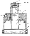
- Figures 4A and 4B show a chip-measuring fixture, which may be used to measure the chips, or substrates, both individually and in a dry stack containing a plurality of chips; Figure 4A showing (in reduced dimensions) the exterior of the complete fixture, including a transducer used as a measuring gauge; and Figure 4B showing (in enlarged dimensions) a vertical plane cross-section through the chip-containing cylinder/piston structure.
- Figures 5A and 5B show the jaw sub-assembly of a fixture suitable for stacking the "wet” (i.e. , epoxy-covered) chips, or substrates, prior to their insertion in the fixture of Figure 3, Figure 5A being a side elevation, and Figure 5B being a cross-section on the line B-B of Figure 5A;
- wet i.e. , epoxy-covered
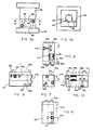
- Figures 6-10 show the final, or "fixed cavity”, lamination fixture, before insertion of the stacked layers, the figures showing, respectively, its top, end, bottom, left side, and right side, views;
- Figures 11 and 12 show the patterns and locations of grooves in the cavity walls which permit the escape of excess epoxy during the curing process
- Figures 13-17 are views corresponding to those of Figures 6-10, except that they show a fixture designed for a "mini-stack" of layers, i e. , a reduced number of layers to be glued together as a partial stack prior to forming the full stack; and
- Figures 18 and 19 show a plan view and a side elevation, respectively, of the assembled fixture of Figures 6-10, in which spring clips are mounted between the screw heads and the side bar members.
- Figure 1 shows a stack 12 comprising a multiplicity of layers 14, each of which is a semiconductor chip (preferably silicon) which carries an integrated circuit having suitable electrical leads terminating at an access plane 16 which, in a photo-detector device, is a front, or focal, plane, on which such leads may be in electrical contact with separate, very- closely-spaced photodetectors.
- the stack 12 is, in effect, a "sandwich” , or laminated structure, comprising numerous silicon chips, or substrates, secured together by suitable adhesive material between adjacent chips.
- the shape of the stack may be described as a rectangular parallelepiped, because each of its surfaces is rectangular. In some cases it may be essentially cubic.
- the stack of chips may be mounted on a supporting block 18, which also functions as a heat-transfer, or cooling, structure, and which may have a mounting stud 20 for use in securing the stack and its supporting block in a larger assembly.
- a supporting block 18 which also functions as a heat-transfer, or cooling, structure, and which may have a mounting stud 20 for use in securing the stack and its supporting block in a larger assembly.
- the combination of the stack of silicon chips and the supporting block is considered to be a module assembly.
- FIG 2 is an exploded view of stack 12, it is seen that it includes separately formed silicon chips 14 which, after being stacked and glued together, are provided on their front, or focal, access back, access plane with back plane wiring 30.
- the present invention deals with the extremely severe requirements of accurately forming the stack of chips, or substrates, so that the electrical leads, particularly those on the front plane, will be properly spaced from one another.
- the requirements which have been encountered in providing focal plane modules, might also be encountered in other situations where densely-packaged electronic circuitry requires access plane connection (to separate contact elements) of very closely spaced electrical leads (i.e., on centers which could be as close as 0.0508mm to 0.1016mm (0.002 to 0.004 inch).
- X-axis alignment places and retaining the chips in position in the direction parallel to the planes of the chips
- Y-axis alignment places and retaining the chips in position in the direction perpendicular to the planes of the chips.
- X-axis alignment holds the electrical leads on the multiplicity of stacked chips in straight "vertical" lines; the correct “horizontal” spacing of such lines depends on accurate forming of the integrated circuitry on the chips.
- the correct "vertical" spacing of the electrical leads in a given vertical line depends on having the active surfaces of the chips essentially equally spaced.
- the stacked chips must be confined in a "fixed cavity", or stack-confining structure, during the process in which the glue, or epoxy, is cured.
- the internal walls, or other position reference elements, of the fixture should provide a predetermined height into which the stacked layer module fits, and may also provide a predetermined volume.
- the confining walls, or position reference elements, which define the cavity, or stack-confining space should be formed of material having a thermal coefficient of expansion as close as possible to that of the chip material.
- the preferred material for this purpose would be molybdenum, which has a thermal expansion coefficient of approximately 4.9 X 10 ⁇ 6/°C (inch/ inch/°C), whereas the thermal expansion coefficient of silicon chips is approximately 4.2 X 10 ⁇ 6/°C (inch/inch/°C).
- Kovar which has a thermal expansion coefficient of 6 X 10 ⁇ 6/°C (inch/inch/°C), has been used because it is more readily available.
- FIG. 3 Before the details of the method are described, attention is called to the fixed cavity structure shown in Figure 3. In that figure, the cavity is closed, except for a final side bar (not shown). A total of six wall-providing members are used in the complete cavity of Figure 3, although it is possible to omit two of the six walls.
- a platform member 32 supports, and is secured by suitable clamping screws to, two "block-shaped" members - a longer block member 34, and a shorter block member 36.
- a cap member 40 which is secured to the platform 32 and block member 34, and which has a raised portion 42 on its inner wall pressing against the flat surfaces of the chips, i.e. , exerting pressure perpendicular to the planes of the chips.
- the final two sides may be closed by two side-bar members, one of which is shown at 44.
- Each side-bar member is secured to the block member 36, and also to the cap member 40. Because the position of cap member 40 is changed as pressure on the stack is increased, the clamping screw which holds each side bar member to the cap member should extend through an appropriately widened slot in the body of the side-bar.
- the chips, or substrates are normally formed by slicing them from wafers of suitable material.
- suitable material is the semiconductor material silicon, but other substrate materials might be used.
- the wafer is initially lapped to provide the desired chip thickness, and to provide identical chip thickness throughout (as tightly controlled as possible). However, analysis and experience have demonstrated that the thickness and flatness of individual chips will vary enough to create major problems in the stacking process.
- the general practice is to form the integrated circuitry on the wafer, lap and polish the wafer down to the appropriate thickness, and then slice each wafer into, say, 36 IC chips. After cleaning, the individual chips intended for a given module are microscopically examined to detect and eliminate any flawed chips. Then the thickness of each chip is measured, under carefully calibrated conditions. The measurement of individual chips permits a selection, preferably using computer-stored thickness and conductor-edge-distance data, of the optimum stacking order for maintaining the electrical lead position tolerance. In other words, a chip slightly over the nominal thickness might be stacked next to a chip slightly under the nominal thickness, in order to avoid a build-up of position deviation.
- FIG. 4A and 4B The fixture used for measurement of chip thickness, both of individual chips and of dry stacked chips (i.e., without epoxy) is shown in Figures 4A and 4B.
- This apparatus is a pressure-operated device which is designed to measure the chips under a predetermined optimum pressure, thus avoiding loss of dimensional reliability. The same pressure may also be used in subsequent process steps.
- the disclosed chip thickness measuring process is capable of measuring them to an accuracy of 0.0025mm (0.0001 inch).
- a chip may have a slightly concave shape, which tends to provide a different thickness measurement if it is pushed into a flatter shape.
- a chip may have a shape which is thicker at one point than another, providing a somewhat wedge-shaped effect in cross-section.
- the apparatus of Figures 4A and 4B is designed to accommodate both of these deviations.
- the solution of the concavity problem is to measure and stack the chips under pressure which is sufficient to essentially flatten them, while minimizing the possibility of damaging them.
- the solution of the wedge-shaped problem is to provide pivoted supporting pads in the apparatus which permit self-leveling of the chips under pressure, thus avoiding damage where the chips cannot be safely flattened.
- a fixture 45 is supported on a stand 47, which also supports a threaded column 49.
- a vertically adjustable arm 51 has one end secured to an internally-threaded collar 53 engaging the threaded column 49 to permit vertical adjustment of the collar and arm.
- the other end of arm 51 has bifurcated clamping extensions 55 which are loosened or tightened by a threaded stem controlled by a knob 57.
- the extensions 55 clamp in position a suitable dimension-measuring gauge.
- a Sony DZ-500 digital gauge has proved suitable for this purpose. It comprises an outer tube 59, in which is telescopically mounted a spring loaded plunger 6l, which carries at its lower end a tip 63 adapted to engage a gauge button on the top of fixture 45.
- the gauge is a transducer which provides a digital readout of the measured dimension on a meter 65, which receives its electrical control signal via wire 67. In making a measurement, the initial readout is reset to zero when the fixture 45 is in its initial "empty" position.
- a receptacle 50 at the top of fixture 45 is provided in which the individual, or stacked, chips are inserted for measurement.
- the chip, or chip stack is supported on a self-leveling platform, or pad, 52 which is pivotally associated with a pin 54, the axis of which extends perpendicular to the plane of the drawing, as seen in Figure 4B.
- the top of the chip, or chip stack is engaged, and placed under downwardly-acting pressure, by a self-leveling pad 56 which is pivotally associated with a pin 58, the axis of which extends parallel to the plane of the drawing, as seen in Figure 4B.
- the rectilinear relationship of the axes of pins 54 and 58 permits leveling of the chips under pressure.
- the fixture 45 may be an air pressure cylinder and piston combination, in which a cylinder housing 60 is bolted to a stationary base 62, and comprises a vertically-extending cylindrical wall 64, and an upper piston-travel-limiting wall 66.
- a piston, or diaphragm, 68 is adapted to reciprocate vertically in the cylinder, and comprises a pressure-responsive movable wall 70, a vertically-extending skirt portion 72 which extends alongside the chip(s), and a cap 74 which carries a gauge button 76 in contact with the tip 63 of the digital gauge. This arrangement permits accurate and precise comparable thickness measurements of the chip(s)
- the pressure at which chip measurement is preferably made is approximately 4.137 ⁇ 106Pa (600 psi), which represents a total force of approximately 65,925ly (150 lbs), on the chip. While this may seem quite high, and while some chip damage is incurred, experience indicates that a relatively high pressure is required for eventual alignment accuracy. Using the same pressure throughout is vital, because it ensures comparability and consistency of the thickness data.
- the selection of chips for use in the stack is based partly on their conformity to the desired thickness and partly on microscopic inspection of their circuitry.
- the yield at present i.e., the percentage of chips suitable for module stacking, may run as low as 5% of the chips originally cut from the wafers. This yield percentage should improve as the I C vendors are able to improve thickness and circuitry consistency.
- a preferred order of chip stacking is determined, using the computer-stored chip thickness data. Then a dry stacking of chips is performed, using the apparatus of Figures 4A and 4B. During this dry stacking, a measurement is taken after each successive chip is added to the stack, in order to compare the actual dimensions to the predicted dimensions. All of these measurements are taken with the same pressure on the chips, i.e., approximately 4.137'106Pa (600 psi). If the measured dimensions do not conform to those desired, chip substitution is required.
- Stacking 128 layers, and curing the epoxy between layers, in a single stack-building sequence creates extreme difficulties in maintaining tolerances in the Y-axis. In other words, a tolerance build-up can occur throughout the entire 128 layer series.
- One means of reducing tolerance problems would be to build completed sub-stacks, each having a smaller number of layers, and then combine the requisite number of sub-stacks to complete the full stack. For example, smaller cavity fixtures, Figures 13 to 17, might be used to stack and cure, say, sixteen chips; then, eight of those stacks could be stacked and cured to complete the 128 layer stack. With the sub-stacks, the tolerance of the lead locations in the stack can be held considerably tighter because of the fact that only a fraction of the total number of chips is subject to the possibility of tolerance build-up.
- the next step is wet stacking. This involves spreading epoxy between the surfaces of adjacent chips.
- the amount of epoxy applied initially is substantially greater than that present in the final module. In other words, a large percentage of the epoxy is "squeezed out" during the final processing.
- wetting of the entire surface of each chip is vital. Air pockets between chips cannot be tolerated. So an excess of epoxy is purposely used, and then it is permitted to escape as necessary.
- a second fixture, or apparatus, termed a "wet stacking" fixture is used to accomplish stacking of the epoxy-covered chips, prior to insertion of the stack in the fixed cavity curing fixture, or apparatus.
- Figures 5A and 5B show the jaw sub-assembly of the wet stacking fixture, which is used to squeeze out excessive glue and to bring the Y-axis dimension to a height 25,4 to 50,8 ⁇ m (1 to 2 mils) greater than the final dimension.
- the jaw sub-assembly is inserted in a suitable press, after the wet chips have been stacked inside the jaw sub-assembly, which comprises (a) a lower jaw 82 having a raised, upwardly-projecting center portion 84 which supports the bottom of the stack, (b) an upper jaw 86 having a raised, downwardly-projecting center portion 88 which presses down on the top of the stack, and (c) side wall members 90 (U-shaped) and 92 (see Figure 5B) secured together by suitable fastening members 94, and enclosing an essentially square (or rectangular) space 96 in which the stacked chips are confined.
- Grooves 98 are provided in each chip-facing wall of the wall members 90 and 92, for the purpose of draining epoxy.
- the epoxy remains liquid until its subsequent curing, so relative sliding motion of the chips is still possible in the wet stacking condition.
- the chips Prior to stacking the chips between the jaws 82 and 86 , they are cleaned, and epoxy is prepared and put in a metering syringe.
- a type of epoxy which has proved satisfactory is Epotek H377, The chips are then stacked one at a time, and after each chip is put in, a metered amount of epoxy is inserted on top of it. The epoxy is applied as a drop and then spread around with a tip of the syringe. During this period, the stack area 96 is open on two sides: on the top and on the vertical side later enclosed by wall member 92.
- each glue line in the completed module should be in the range of 0,508 to 2,54 ⁇ m (0.02 to 0.10 mil). This dimension is determined by subtracting the total thickness of the dry stacked chips, say 12,9mm (508 mils), from the Y-dimension of the fixed cavity, say 13,11mm (516 mils), and then dividing the difference 203 ⁇ m (8 mils) by the number of glue lines (127 in a 128 chip module), which gives an average glue line thickness of approximately 1,524 ⁇ m (0.06 mil).
- a small tool which may be made of Teflon and have a shape similar to that of a tongue depressor, may be used to gently push the chips into the space 96. This provides some preliminary alignment of the chips.
- the wall member 92 is secured to the U-shaped wall member 90, leaving only the top of the stack open.
- the upper jaw 86 is then put into position, with its center portion 88 engaging the top of the stack.
- the jaw sub-assembly is then inserted in a suitable press (not shown), and pressure is applied between the upper and lower jaws 86 and 82 to compress the wet stack of chips. The pressure causes the upper jaw to move downward until its motion is stopped by engagement with the side walls 90 and 92.
- the wall members are provided to enclose the stack when it is being cured in a suitable oven, preferably at a temperature in the range of 120-150°C, for a period in the range of 1-3 hours. It is considered necessary that the wall members each be formed of material having a thermal coefficient of expansion similar to that of the chip material.
- Kovar is a suitable wall material in a fixture which encloses a silicon chip stack. A stress-relieving process should be used in the fabrication of the Kovar wall members. They are first rough-machined, then raised to a very high temperature and returned to room temperature to relieve the stress. Thereafter, the Kovar wall members receive final machining to the very precise dimensions required.
- Figure 6 may be considered a top view, Figure 7 an end view, Figure 8 a bottom view, and Figures 9 and 10 side views. This orientation is applied during assembling of the fixture; but preferably the end opposite to the end seen in Figure 7 will be oriented downwards so that the chips will be horizontal during curing.
- the platform wall member 32a which is seen at the bottom of Figures 9 and 10, provides support for the longer block member 34a (Fig. 9) and for the shorter block member 36a (Fig. 10).
- the mounting of members 34a and 36a on platform member 32a closes three sides of the cavity 38.
- Each member is secured to each adjoining member by a least one screw 100, after initial alignment by one or more dowel pins 102.
- the heads of the screws 100 need to be recessed in at least two outside surfaces of the fixture, both of which are used as bottom surfaces during the assembling procedure.
- each screw 100 extends through an enlarged threaded opening 104 in the near member, which it does not engage, into threaded engagement with a smaller threaded opening 106 in the far member. This permits a larger back-off screw to be threaded 10 into the opening during disassembly of the fixture.
- the back-off screw when it engages the far member, causes the near and far members to separate.
- mold release material is used to cover thoroughly the interior of the cavity.
- a preferred procedure for ensuring effective application of mold release material includes the following steps: (a) clean the cavity; (b) heat the fixture (including unassembled wall members); (c) coat its entire interior (including unassembled wall members) with mold release material (brushed on); (d) dry the fixture; (e) reheat it; and (f) apply another coat of mold release material.
- the wet stack of chips is removed from the wet stacking fixture ( Figures 5A and 5B), and inserted into the cavity of the final fixture (after wiping off excess epoxy). With the cavity in the position shown in Figure 10, the planes of the stacked chips will extend essentially vertically.
- Alignment of the chips in the X-axis is accomplished by orienting the stacked chips in the cavity in such a way that: (a) their access place edges (i.e., their electrical-lead-providing edges) are facing upwardly (as seen in Figure 10), and (b) the sides of the chips are aligned against the cavity wall 110 provided by the longer block member 34a (see Figure 6). Thus the plane of the module opposite the access plane rests on the platform member 32a.
- the X-alignment of the chips is ensured by pushing them individually against the wall 110, preferably using the same Teflon-coated tool which was used during wet stacking.
- the cap member 40a whose raised surface 42a pushes against the stacked chips in a direction perpendicular to the planes of the chips, may already have been added to the fixture, but not tightened down to its final position.
- the other two cavity wall members are two side bar members 44a and 45a, which are shown in dashed lines in the figures.
- the screws 100 which secure them to cap member 40a and block member 36a should extend through oversize holes in members 44a and 45a, in order to prevent damaging the stacked chips if they move relative to members 44a and 45a. Also, it is desirable that the screw 100 (see Figures 18 and 19) exert a resilient, rather than a rigid, retention pressure against side bar members 44a and 45a.
- FIGS 18 and 19 illustrate the preferred side bar retention arrangement.
- the screw 100 is shown in place at the right side of the figures, but is omitted at the left side of the figures.
- an oversize hole 101, and a "standoff" member 103 are shown.
- a spring clip 105 is shown, between the side bar member and the head of screw 100. The screw 100 is tightened down until it engages the standoff member 103. Thereafter, the spring clip 105 provides a resilient retention force against the side bar member.
- the Kovar parts which enclose the fixed cavity 38 are carefully built to provide the exact dimensions desired. In preliminary assembly for measurement purposes, a certain level of torque is applied in tightening the screws 100. Development work has demonstrated that the desired dimensions of the cavity can be slightly altered if final assembly of the Kovar parts is performed using a different torque on the screws. Since correct dimensions of the cavity during curing are a vital requirement for success, it is considered important to use substantially the same scew-tightening torque during final assembly as that used during fabrication of the assembly parts by the machinist. It appears that the preferred tightening torque is about 1.99 ⁇ m (17.6 inch-pounds), because that torque produces repeatable cavity dimensions.
- the entire assembly is placed in an oven, and heated at a temperature, and for a period, suitable for curing the epoxy, thereby providing a completed, integrated module.
- a suitable temperature range for curing is 120° to 150°C and a suitable period range is 1 to 3 hours.
- the fixture should be so oriented that the chip planes are substantially horizontal. In other words, the right end 112 of the fixture, as seen in Figure 10 (or the left end, as seen in Figure 9) would be the bottom surface during curing. The purpose of this orientation is to prevent non-uniform leakage of epoxy from its position between the chips.
- FIG. 11 and 12 show appropriate epoxy-draining grooves.
- Figure 11 shows a "waffle" pattern, suitable for use at the top and bottom walls of the stack, i.e. , walls extending in planes parallel to the chip planes, and being used to press the chips together.
- the flat chip surfaces of the end chips are supported on the raised "islands" 114.
- Epoxy is allowed to drain through the network of interconnecting grooves 116.
- Figure 12 shows a pattern suitable for use in each of the four walls which engage edges of the stacked chips. Chip wall engagement is against longitudinally extending ridges 118. The remaining area is available for epoxy draining, including longitudinally extending grooves 120, and the entire recessed center portion 122.
- the first step would bring the cavity-enclosed stack to sufficient cohesion to prevent chip displacement.
- the stack would then be removed from the cavity, and the final curing would be accomplished with the stack as a free-standing unit.
- Figures 13 to 17 show the wall members of a fixture used to provide a "mini-stack" containing 16 layers, instead of 128 layers.
- the wall-providing members in Figures 13 to 17 have the same numerals as corresponding members in previous figures, except that the suffix "b" has been used. Because the Y-axis dimension of the stack in Figures 13 to 17 is only one-eighth of the comparable dimension in Figures 6 to 10, the dimension of cavity 38b, between surface 42b (on cap member 40b) and the inner end of the shorter block member 36b, is one-eighth that of the cavity 38 in Figures 6 to 10.
- the length of the shorter block member 36b is increased to fill the remaining seven-eighths of the cavity length.
- several of them can then be stacked in a full-size cavity and secured together to form a full stack. This requires that the original epoxy be able to withstand two curing procedures, which has proved to be feasible.
Landscapes
- Encapsulation Of And Coatings For Semiconductor Or Solid State Devices (AREA)
- Container, Conveyance, Adherence, Positioning, Of Wafer (AREA)
Claims (8)
- Bei der Herstellung eines Trägerstapels (12) für elektronische Schaltungen aus Schichten (14), die sich jeweils in einer Ebene senkrecht zu einer Zugangsebene an einem Endabschnitt des Stapels (12) erstrecken und jeweils mehrere beabstandete elektrische Leitungen an der Zugangsebene (16) aufweisen, wobei diese Leitungen Teil eines zweidimensionalen planaren Feldes mit der X-Achse parallel zu den Schichtebenen und der Y-Achse senkrecht zu den Schichtebenen sind, umfaßt das Verfahren:
Ausbilden mehrerer Substratschichten (14), jeweils mit einer Schaltung darauf, die an dem Endabschnitt der Zugangsebene (16) mehrere separarate elektrische Leitungen aufweisen, welche entlang der X-Achse des Feldes beabstandet sind;
Messen der Dicke einer jeden Schicht (14); Festlegen einer Reihenfolge, und zwar auf der Grundlage der Messungen der Schichtdicken, in der die Schichten (14) übereinander anzuordnen sind, so daß die elektrischen Leitungen der Zugangsebene an den gewünschten stellen der Y-Achse des Feldes angeordnet werden;
Herstellen einer Stapel-Festlegungsstruktur, die (a) obere und untere Wandteile (82, 86), deren Oberflächen mit den oberen und unteren Schichten (14) des Stapels (12) in Eingriff kommen werden, um die Y-Achsen-Ausdehnung zu bestimmen, und (b) mehrere Positionsbezugselemente senkrecht zu den Wandteilen (82, 86) aufweist, die dazu dienen, die X-Achsen-Ausrichtung mindestens zweier Seiten der Schichten (14) festzulegen;
Naßstapeln der Schichten (14) in der vorbestimmten Ordnung, nachdem in wesentlichen die gleiche Menge eines flüssigen Klebstoffes zwischen Jedem Paar benachbarter Schichten (14) angebracht worden ist;
Anordnen der Schichten (14) in der Stapel-Festlegungsstruktur, getragen auf dem unteren Wandteil (82); Ausrichten der Schichten (14) entlang der X-Achse durch In-Eingriff-Bringen derselben mit den Positionsbezugselementen der Stapel-Festlegungsstruktur;
Verwenden der oberen und unteren Wandteile (82, 86) der Stapel-Festlegungsstruktur, um Druck entlang der Y-Achse auszuüben, wodurch die Y-Achsen-Ausdehnung des Stapels (12) dazu gebracht wird, der gewünschten endgültigen Ausdehnung zu entprechen; und Aussetzen des festgelegten Stapels (12) einer Wärme, um zu bewirken, daß der flüssige Klebstoff die Schichten (14) in einem integrierten Stapel sichert. - Verfahren nach Anspruch 1, das ferner umfaßt:
Hinzufügen mehrerer zusätzlicher Positionsbezugselemente zu der Stapel-Festlegungsstruktur nach dem Ausrichten der Schichten (14), um den Stapel (12) während des Erhitzens ganz in einem unveränderlichen Raum festzulegen. - Verfahren nach Anspruch 1, wobei die Y-Achsen-Ausdehnung der Stapel-Festlegungsstruktur von Elementen überwacht wird, die einen thermischen Ausdehnungskoeffizienten haben, welcher demjenigen des Schichtwerkstoffes nahekommt.
- Verfahren nach Anspruch 1 oder 2, wobei:
Drei Seiten (32a, 34a, 36a) der Stapel-Festlegungsstruktur zuerst zusammengesetzt werden, wobei die Struktur auf drei Seiten unbegrenzt bleibt;
die Schichten (14) sodann in die Struktur eingesetzt werden, wobei ihre Zugangsebenen-Enden für die Ausrichtungskontrolle sichtbar sind;
Die Schichten (14) entlang der X-Achse in Eingriff gegen das Bezugselement auf einer Seite gedrückt werden; und
die X-Achsen-Ausrichtung durch die mikroskopische Kontrolle der Zugangsebene geprüft wird. - Verfahren nach Anspruch 4, wobei:
Nach der X-Achsen-Ausrichtung die verbleibenden drei Seiten (40a, 42a; 44a; 45a) der Stapel-Festlegungsstruktur zusammengesetzt werden; und eine (40a, 42a) der letzten drei Seiten dazu gebrach wird, Druck entlang der Y-Achse auf den Stapel auszuüben. - Verfahren nach Anspruch 1, 2 oder 5, wobei:
eine Überschußmenge flüssigen Klebstoffes verwendet wird, um unbrauchbaren Bereichen zwischen Schichten (14) vorzubeugen; und
es dem überschüssigen flüssigen Klebstoff ermöglicht wird, aus dem Stapel (12) herauszugelangen. - Verfahren nach Anspruch 1 oder Anspruch 2, das ferne umfaßt:
Stapeln mehrerer integrierter Mehrschicht-Stapel (12 zu einer Mehrstapel-Kombination;
Anbringen flüssigen Klebstoffes zwischen benachbarte Stapeln (12);
Halten der Mehrstapel-Kombination in einer Stapel-Festlegungsstruktur;
Ausrichten der Stapel (12) in der X-Achse;
Ausüben von Druck entlang der Y-Achse, um zu bewirken, daß die Y-Achsen-Ausdehnung der gewünschten endgültigen Ausdehnung entspricht; und
Aussetzen der festgelegten Mehrstapel-Kombination einer Wärme, um zu bewirken, daß der flüssige Klebstoff die Stapel (12) in einer integrierten Kombination mehrschichtiger Stapel sichert. - Verfahren nach Anspruch 1 oder 2, das ferner umfaßt:
Aufbringen von Formlösewerkstoff auf die Schichtanlageflächen der Stapel-Festlegungsstruktur, bevor die Schichten (14) in der Struktur angeordnet werden.
Priority Applications (1)
| Application Number | Priority Date | Filing Date | Title |
|---|---|---|---|
| AT85906123T ATE61159T1 (de) | 1984-11-23 | 1985-11-20 | Verfahren zur herstellung von modulen, aufgestapelte integrierte schaltungen enthalten. |
Applications Claiming Priority (2)
| Application Number | Priority Date | Filing Date | Title |
|---|---|---|---|
| US06/674,096 US4617160A (en) | 1984-11-23 | 1984-11-23 | Method for fabricating modules comprising uniformly stacked, aligned circuit-carrying layers |
| US674096 | 1984-11-23 |
Publications (3)
| Publication Number | Publication Date |
|---|---|
| EP0204767A1 EP0204767A1 (de) | 1986-12-17 |
| EP0204767A4 EP0204767A4 (de) | 1988-03-22 |
| EP0204767B1 true EP0204767B1 (de) | 1991-02-27 |
Family
ID=24705277
Family Applications (1)
| Application Number | Title | Priority Date | Filing Date |
|---|---|---|---|
| EP85906123A Expired - Lifetime EP0204767B1 (de) | 1984-11-23 | 1985-11-20 | Verfahren zur herstellung von modulen, aufgestapelte integrierte schaltungen enthalten |
Country Status (5)
| Country | Link |
|---|---|
| US (1) | US4617160A (de) |
| EP (1) | EP0204767B1 (de) |
| JP (1) | JPH0828465B2 (de) |
| DE (1) | DE3581937D1 (de) |
| WO (1) | WO1986003338A1 (de) |
Families Citing this family (53)
| Publication number | Priority date | Publication date | Assignee | Title |
|---|---|---|---|---|
| US4704319A (en) * | 1984-11-23 | 1987-11-03 | Irvine Sensors Corporation | Apparatus and method for fabricating modules comprising stacked circuit-carrying layers |
| US4695716A (en) * | 1985-12-13 | 1987-09-22 | Xerox Corporation | Image sensor array for assembly with like arrays to form a longer array |
| US4706166A (en) * | 1986-04-25 | 1987-11-10 | Irvine Sensors Corporation | High-density electronic modules--process and product |
| US4943334A (en) * | 1986-09-15 | 1990-07-24 | Compositech Ltd. | Method for making reinforced plastic laminates for use in the production of circuit boards |
| US4779005A (en) * | 1987-05-11 | 1988-10-18 | Irvine Sensors Corporation | Multiple detector viewing of pixels using parallel time delay and integration circuitry |
| WO1989004113A1 (en) * | 1987-10-20 | 1989-05-05 | Irvine Sensors Corporation | High-density electronic modules, process and product |
| US5354695A (en) | 1992-04-08 | 1994-10-11 | Leedy Glenn J | Membrane dielectric isolation IC fabrication |
| WO1990011613A1 (en) * | 1989-03-27 | 1990-10-04 | Irvine Sensors Corporation | Analog to digital conversion incorporated in z-technology module |
| DE69030195T2 (de) * | 1989-07-07 | 1997-06-19 | Irvine Sensors Corp | Fabrikation einer elektronischen schaltungseinheit, welche gestapelte ic-lagen mit umleitungsleitungen enthält |
| US4959749A (en) * | 1989-08-16 | 1990-09-25 | Unisys Corporation | Layered electronic assembly having compensation for chips of different thickness and different I/O lead offsets |
| DE4031795C1 (de) * | 1990-10-08 | 1991-11-28 | Degussa Ag, 6000 Frankfurt, De | |
| US5075201A (en) * | 1990-10-31 | 1991-12-24 | Grumman Aerospace Corporation | Method for aligning high density infrared detector arrays |
| US5149671A (en) * | 1990-12-03 | 1992-09-22 | Grumman Aerospace Corporation | Method for forming multilayer indium bump contact |
| US5270485A (en) * | 1991-01-28 | 1993-12-14 | Sarcos Group | High density, three-dimensional, intercoupled circuit structure |
| US5379191A (en) * | 1991-02-26 | 1995-01-03 | Microelectronics And Computer Technology Corporation | Compact adapter package providing peripheral to area translation for an integrated circuit chip |
| US5239447A (en) * | 1991-09-13 | 1993-08-24 | International Business Machines Corporation | Stepped electronic device package |
| US5420055A (en) * | 1992-01-22 | 1995-05-30 | Kopin Corporation | Reduction of parasitic effects in floating body MOSFETs |
| US6714625B1 (en) | 1992-04-08 | 2004-03-30 | Elm Technology Corporation | Lithography device for semiconductor circuit pattern generation |
| US5985693A (en) * | 1994-09-30 | 1999-11-16 | Elm Technology Corporation | High density three-dimensional IC interconnection |
| US5279991A (en) * | 1992-05-15 | 1994-01-18 | Irvine Sensors Corporation | Method for fabricating stacks of IC chips by segmenting a larger stack |
| US5327327A (en) * | 1992-10-30 | 1994-07-05 | Texas Instruments Incorporated | Three dimensional assembly of integrated circuit chips |
| US5737192A (en) * | 1993-04-30 | 1998-04-07 | The United States Of America As Represented By The Secretary Of The Air Force | Density improvement in integration modules |
| US5432681A (en) * | 1993-04-30 | 1995-07-11 | The United States Of America As Represented By The Secretary Of The Air Force | Density improvement for planar hybrid wafer scale integration |
| US5561593A (en) * | 1994-01-27 | 1996-10-01 | Vicon Enterprises, Inc. | Z-interface-board |
| WO1995025341A1 (en) * | 1994-03-15 | 1995-09-21 | Irvine Sensors Corporation | 3d stack of ic chips having leads reached by vias through passivation covering access plane |
| US5635010A (en) * | 1995-04-14 | 1997-06-03 | Pepe; Angel A. | Dry adhesive joining of layers of electronic devices |
| US5732462A (en) * | 1995-05-30 | 1998-03-31 | International Business Machines Corporation | Fixture for assembling electronic circuit modules |
| US5892203A (en) * | 1996-05-29 | 1999-04-06 | International Business Machines Corporation | Apparatus for making laminated integrated circuit devices |
| US6551857B2 (en) | 1997-04-04 | 2003-04-22 | Elm Technology Corporation | Three dimensional structure integrated circuits |
| US5915167A (en) | 1997-04-04 | 1999-06-22 | Elm Technology Corporation | Three dimensional structure memory |
| US5904502A (en) * | 1997-09-04 | 1999-05-18 | International Business Machines Corporation | Multiple 3-dimensional semiconductor device processing method and apparatus |
| US6984571B1 (en) * | 1999-10-01 | 2006-01-10 | Ziptronix, Inc. | Three dimensional device integration method and integrated device |
| US6500694B1 (en) * | 2000-03-22 | 2002-12-31 | Ziptronix, Inc. | Three dimensional device integration method and integrated device |
| US6902987B1 (en) * | 2000-02-16 | 2005-06-07 | Ziptronix, Inc. | Method for low temperature bonding and bonded structure |
| JP2001352035A (ja) * | 2000-06-07 | 2001-12-21 | Sony Corp | 多層半導体装置の組立治具及び多層半導体装置の製造方法 |
| US6563133B1 (en) | 2000-08-09 | 2003-05-13 | Ziptronix, Inc. | Method of epitaxial-like wafer bonding at low temperature and bonded structure |
| US6748994B2 (en) | 2001-04-11 | 2004-06-15 | Avery Dennison Corporation | Label applicator, method and label therefor |
| US6831370B2 (en) * | 2001-07-19 | 2004-12-14 | Micron Technology, Inc. | Method of using foamed insulators in three dimensional multichip structures |
| US6433413B1 (en) | 2001-08-17 | 2002-08-13 | Micron Technology, Inc. | Three-dimensional multichip module |
| US6635960B2 (en) * | 2001-08-30 | 2003-10-21 | Micron Technology, Inc. | Angled edge connections for multichip structures |
| US6747347B2 (en) * | 2001-08-30 | 2004-06-08 | Micron Technology, Inc. | Multi-chip electronic package and cooling system |
| US6686654B2 (en) * | 2001-08-31 | 2004-02-03 | Micron Technology, Inc. | Multiple chip stack structure and cooling system |
| US6717061B2 (en) | 2001-09-07 | 2004-04-06 | Irvine Sensors Corporation | Stacking of multilayer modules |
| US6560109B2 (en) | 2001-09-07 | 2003-05-06 | Irvine Sensors Corporation | Stack of multilayer modules with heat-focusing metal layer |
| US6734370B2 (en) * | 2001-09-07 | 2004-05-11 | Irvine Sensors Corporation | Multilayer modules with flexible substrates |
| US6620638B1 (en) | 2002-06-05 | 2003-09-16 | Micron Technology, Inc. | Testing of multi-chip electronic modules |
| WO2004015764A2 (en) | 2002-08-08 | 2004-02-19 | Leedy Glenn J | Vertical system integration |
| US7109092B2 (en) | 2003-05-19 | 2006-09-19 | Ziptronix, Inc. | Method of room temperature covalent bonding |
| US20050046034A1 (en) * | 2003-09-03 | 2005-03-03 | Micron Technology, Inc. | Apparatus and method for high density multi-chip structures |
| US6993835B2 (en) * | 2003-12-04 | 2006-02-07 | Irvine Sensors Corp. | Method for electrical interconnection of angularly disposed conductive patterns |
| USD538315S1 (en) * | 2004-10-26 | 2007-03-13 | Urban Manufacturing, Inc. | Collet holder and tool body |
| JP6707292B2 (ja) * | 2016-10-14 | 2020-06-10 | 株式会社ディスコ | 積層チップの製造方法 |
| KR20230097121A (ko) | 2020-10-29 | 2023-06-30 | 아데이아 세미컨덕터 본딩 테크놀로지스 인코포레이티드 | 직접 접합 방법 및 구조체 |
Family Cites Families (11)
| Publication number | Priority date | Publication date | Assignee | Title |
|---|---|---|---|---|
| US3284884A (en) * | 1965-02-01 | 1966-11-15 | Nat Video Corp | Assembly jig for positioning photographic shadow masks in color television picture tube face plates |
| JPS5810437B2 (ja) * | 1974-12-20 | 1983-02-25 | ジェイエスアール株式会社 | ネツユウチヤクホウホウ |
| US4128235A (en) * | 1977-09-01 | 1978-12-05 | United Aircraft Products, Inc. | Braze fixture |
| US4186916A (en) * | 1978-09-18 | 1980-02-05 | Salisbury Special Tool | Precision workpiece positioning means for machine tools |
| US4342090A (en) * | 1980-06-27 | 1982-07-27 | International Business Machines Corp. | Batch chip placement system |
| US4551629A (en) * | 1980-09-16 | 1985-11-05 | Irvine Sensors Corporation | Detector array module-structure and fabrication |
| US4525921A (en) * | 1981-07-13 | 1985-07-02 | Irvine Sensors Corporation | High-density electronic processing package-structure and fabrication |
| JPS58103149A (ja) * | 1981-12-15 | 1983-06-20 | Matsushita Electric Works Ltd | 半導体装置 |
| JPS58188243A (ja) * | 1982-04-23 | 1983-11-02 | Canon Inc | 複写材シ−ト給送装置 |
| US4506442A (en) * | 1982-09-29 | 1985-03-26 | Lenkeit Industries, Inc. | Method and apparatus for stacking a plurality of laminate layers to form a composite board |
| US4536239A (en) * | 1983-07-18 | 1985-08-20 | Nicolet Instrument Corporation | Multi-layer circuit board inspection system |
-
1984
- 1984-11-23 US US06/674,096 patent/US4617160A/en not_active Expired - Lifetime
-
1985
- 1985-11-20 DE DE8585906123T patent/DE3581937D1/de not_active Expired - Lifetime
- 1985-11-20 EP EP85906123A patent/EP0204767B1/de not_active Expired - Lifetime
- 1985-11-20 JP JP60505387A patent/JPH0828465B2/ja not_active Expired - Lifetime
- 1985-11-20 WO PCT/US1985/002298 patent/WO1986003338A1/en not_active Ceased
Also Published As
| Publication number | Publication date |
|---|---|
| JPH0828465B2 (ja) | 1996-03-21 |
| JPS62500901A (ja) | 1987-04-09 |
| US4617160A (en) | 1986-10-14 |
| EP0204767A4 (de) | 1988-03-22 |
| WO1986003338A1 (en) | 1986-06-05 |
| EP0204767A1 (de) | 1986-12-17 |
| DE3581937D1 (de) | 1991-04-04 |
Similar Documents
| Publication | Publication Date | Title |
|---|---|---|
| EP0204767B1 (de) | Verfahren zur herstellung von modulen, aufgestapelte integrierte schaltungen enthalten | |
| US4704319A (en) | Apparatus and method for fabricating modules comprising stacked circuit-carrying layers | |
| US6080603A (en) | Fixtures and methods for lead bonding and deformation | |
| US5654877A (en) | Lead-on-chip integrated circuit apparatus | |
| US5221642A (en) | Lead-on-chip integrated circuit fabrication method | |
| US6064217A (en) | Fine pitch contact device employing a compliant conductive polymer bump | |
| US8044673B1 (en) | Method and apparatus for positioning and contacting singulated semiconductor dies | |
| US6468098B1 (en) | Electrical contactor especially wafer level contactor using fluid pressure | |
| TW498533B (en) | Semiconductor device and its manufacturing method | |
| US20020011859A1 (en) | Method for forming conductive bumps for the purpose of contrructing a fine pitch test device | |
| GB2057757A (en) | Moulded lead frame dual in-line package and fabrication method therefor | |
| JPH02231753A (ja) | 集積回路アセンブリ | |
| JPH07191091A (ja) | 電気接続装置 | |
| US5414372A (en) | Reusable test apparatus for integrated circuit chips | |
| KR101785092B1 (ko) | 레이저를 이용한 반도체 본딩장치 | |
| TW201027647A (en) | Methods, apparatus and articles of manufacture for testing a plurality of singulated die | |
| US6440771B1 (en) | Method for constructing a wafer interposer by using conductive columns | |
| US4184623A (en) | Process for bonding circuit modules onto a thin-film circuit | |
| US9305894B2 (en) | Constrained die adhesion cure process | |
| RU2498449C1 (ru) | Контактирующее устройство | |
| US6508845B1 (en) | Method and apparatus for precoining BGA type packages prior to electrical characterization | |
| EP0637079A1 (de) | Verbesserter Mehrchipmodul | |
| JP2000187060A (ja) | 電子部品試験装置 | |
| IL80785A (en) | Compressive pedestal for microminiature connections | |
| KR100261942B1 (ko) | 반도체 다이스를 테스팅하기 위한 방법 |
Legal Events
| Date | Code | Title | Description |
|---|---|---|---|
| PUAI | Public reference made under article 153(3) epc to a published international application that has entered the european phase |
Free format text: ORIGINAL CODE: 0009012 |
|
| 17P | Request for examination filed |
Effective date: 19860801 |
|
| AK | Designated contracting states |
Kind code of ref document: A1 Designated state(s): AT BE CH DE FR GB LI NL SE |
|
| A4 | Supplementary search report drawn up and despatched |
Effective date: 19880322 |
|
| 17Q | First examination report despatched |
Effective date: 19900305 |
|
| GRAA | (expected) grant |
Free format text: ORIGINAL CODE: 0009210 |
|
| AK | Designated contracting states |
Kind code of ref document: B1 Designated state(s): AT BE CH DE FR GB LI NL SE |
|
| PG25 | Lapsed in a contracting state [announced via postgrant information from national office to epo] |
Ref country code: SE Effective date: 19910227 Ref country code: LI Effective date: 19910227 Ref country code: CH Effective date: 19910227 Ref country code: BE Effective date: 19910227 Ref country code: AT Effective date: 19910227 |
|
| REF | Corresponds to: |
Ref document number: 61159 Country of ref document: AT Date of ref document: 19910315 Kind code of ref document: T |
|
| REF | Corresponds to: |
Ref document number: 3581937 Country of ref document: DE Date of ref document: 19910404 |
|
| REG | Reference to a national code |
Ref country code: CH Ref legal event code: PL |
|
| ET | Fr: translation filed | ||
| PLBE | No opposition filed within time limit |
Free format text: ORIGINAL CODE: 0009261 |
|
| STAA | Information on the status of an ep patent application or granted ep patent |
Free format text: STATUS: NO OPPOSITION FILED WITHIN TIME LIMIT |
|
| 26N | No opposition filed | ||
| PGFP | Annual fee paid to national office [announced via postgrant information from national office to epo] |
Ref country code: NL Payment date: 19961231 Year of fee payment: 12 |
|
| PG25 | Lapsed in a contracting state [announced via postgrant information from national office to epo] |
Ref country code: NL Free format text: LAPSE BECAUSE OF NON-PAYMENT OF DUE FEES Effective date: 19980601 |
|
| NLV4 | Nl: lapsed or anulled due to non-payment of the annual fee |
Effective date: 19980601 |
|
| REG | Reference to a national code |
Ref country code: GB Ref legal event code: IF02 |
|
| PGFP | Annual fee paid to national office [announced via postgrant information from national office to epo] |
Ref country code: FR Payment date: 20021108 Year of fee payment: 18 |
|
| PGFP | Annual fee paid to national office [announced via postgrant information from national office to epo] |
Ref country code: GB Payment date: 20021120 Year of fee payment: 18 |
|
| PGFP | Annual fee paid to national office [announced via postgrant information from national office to epo] |
Ref country code: DE Payment date: 20021121 Year of fee payment: 18 |
|
| PG25 | Lapsed in a contracting state [announced via postgrant information from national office to epo] |
Ref country code: GB Free format text: LAPSE BECAUSE OF NON-PAYMENT OF DUE FEES Effective date: 20031120 |
|
| PG25 | Lapsed in a contracting state [announced via postgrant information from national office to epo] |
Ref country code: DE Free format text: LAPSE BECAUSE OF NON-PAYMENT OF DUE FEES Effective date: 20040602 |
|
| GBPC | Gb: european patent ceased through non-payment of renewal fee |
Effective date: 20031120 |
|
| PG25 | Lapsed in a contracting state [announced via postgrant information from national office to epo] |
Ref country code: FR Free format text: LAPSE BECAUSE OF NON-PAYMENT OF DUE FEES Effective date: 20040730 |
|
| REG | Reference to a national code |
Ref country code: FR Ref legal event code: ST |