EP0200592A1 - Handgesteuerter statischer Schalter - Google Patents
Handgesteuerter statischer Schalter Download PDFInfo
- Publication number
- EP0200592A1 EP0200592A1 EP86400631A EP86400631A EP0200592A1 EP 0200592 A1 EP0200592 A1 EP 0200592A1 EP 86400631 A EP86400631 A EP 86400631A EP 86400631 A EP86400631 A EP 86400631A EP 0200592 A1 EP0200592 A1 EP 0200592A1
- Authority
- EP
- European Patent Office
- Prior art keywords
- groove
- receiver
- fact
- bottom wall
- transmitter
- Prior art date
- Legal status (The legal status is an assumption and is not a legal conclusion. Google has not performed a legal analysis and makes no representation as to the accuracy of the status listed.)
- Withdrawn
Links
Images

Classifications
-
- H—ELECTRICITY
- H03—ELECTRONIC CIRCUITRY
- H03K—PULSE TECHNIQUE
- H03K17/00—Electronic switching or gating, i.e. not by contact-making and –breaking
- H03K17/94—Electronic switching or gating, i.e. not by contact-making and –breaking characterised by the way in which the control signals are generated
- H03K17/941—Electronic switching or gating, i.e. not by contact-making and –breaking characterised by the way in which the control signals are generated using an optical detector
-
- H—ELECTRICITY
- H03—ELECTRONIC CIRCUITRY
- H03K—PULSE TECHNIQUE
- H03K17/00—Electronic switching or gating, i.e. not by contact-making and –breaking
- H03K17/18—Modifications for indicating state of switch
-
- H—ELECTRICITY
- H03—ELECTRONIC CIRCUITRY
- H03K—PULSE TECHNIQUE
- H03K2217/00—Indexing scheme related to electronic switching or gating, i.e. not by contact-making or -breaking covered by H03K17/00
- H03K2217/94—Indexing scheme related to electronic switching or gating, i.e. not by contact-making or -breaking covered by H03K17/00 characterised by the way in which the control signal is generated
- H03K2217/941—Indexing scheme related to electronic switching or gating, i.e. not by contact-making or -breaking covered by H03K17/00 characterised by the way in which the control signal is generated using an optical detector
- H03K2217/94102—Indexing scheme related to electronic switching or gating, i.e. not by contact-making or -breaking covered by H03K17/00 characterised by the way in which the control signal is generated using an optical detector characterised by the type of activation
- H03K2217/94104—Indexing scheme related to electronic switching or gating, i.e. not by contact-making or -breaking covered by H03K17/00 characterised by the way in which the control signal is generated using an optical detector characterised by the type of activation using a light barrier
Definitions
- the present invention relates to static switches of the manual control type, that is to say all devices which make it possible to deliver to at least one output terminal a signal capable of taking at least two levels, one of the two levels being obtained when for example, an element is applied manually at a determined location. It also relates to the application of these switches to the sequential control of elements, for example electronic, as a function of a determined position of an element which can be moved manually.
- switches like the ones defined above that can be controlled manually.
- they comprise under a flexible wall two contacts arranged one opposite the other, and subjected to the action of repulsion spring means, for example of a material which is not electrically conductive.
- repulsion spring means for example of a material which is not electrically conductive.
- To control such a switch it suffices, for example directly or indirectly with a finger, to exert a light pressure on the flexible wall to bring the two contacts into contact which then establish the switching function, for example for the closing of a circuit.
- This system gives good results but nevertheless requires precautions for use, because excessive pressure forces can lead more or less quickly to the destruction of the contacts, especially in particular applications, such as for example the control of different musical elements in performance halls where the devices are often subjected to severe manipulation tests.
- the object of the present invention is to provide a switch of the static type, advantageously manually controllable, reliable, making it possible to give potential users sensations of touch, allowing them, moreover, to know whether the switching has been carried out and, more particularly, in a multi-switching system, which switching has been carried out.
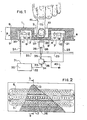
- the device illustrated relates to a static type switch as defined in the preamble to the description, a switch which is capable of being controlled manually, in particular by applying a finger, as it appears - schematically in Figure 1.
- the switch comprises a body 1, preferably made of a transparent material such as, for example, a plastic material, in which a groove 2 and two grooves 6 and 7 are made.
- the groove 2 is delimited laterally by two walls 3 and 4 and by a bottom 5, the two walls 3 and 4, preferably parallel, separating the groove 2 respectively from the two grooves 6 and 7.
- the body 1 has a substantially flat shape delimited by two substantially parallel faces 8 and 9. From this fact and in this embodiment, the groove 2 has its opening 10 on the face 8 of the body 1, while the two grooves 6 and 7 have their respective opening 11 and 12 facing the face 9.
- the groove 2 and the two grooves 6 and 7 produced in this plate-shaped body 1 are produced so that the thickness of the side walls 3 and 4 and of the bottom wall 5 is sufficient to be able to withstand pressures which can be exerted by a finger, even of high intensity, but nevertheless sufficiently thin to allow a beam of visible electromagnetic waves, for example of the order of 6,000 Angstroms or not visible, for example of 10,600 Angstroms, to pass through this material without undergoing significant attenuation.
- this radiation will be chosen in the invisible domain, such as for example that emitted by an AsGa laser diode.
- the switch comprises at least one emitter of electromagnetic waves 13 arranged in the groove 6 so that its emitting surface 14 is capable of emitting the beam of electromagnetic waves 15 on the optical axis 16 which, as shown in FIGS. 1 and 2, is substantially perpendicular to the two side walls 3 and 4 which, themselves, are advantageously parallel and so that this optical axis passes substantially in the middle of the other groove 7 and therefore also in the middle of the groove 2. Therefore, when the transmitter 13 emits its beam 15, it can propagate along the axis 16 through the two side walls 3 and 4 and fall into the groove 7 if no obstacle is present in the groove 2.
- a receiver sensitive 17 to electromagnetic radiation emitted by the transmitter 13.
- This sensitive receiver 17 is itself capable of delivering at its output 18 a signal generally of electrical form the value of the amplitude of which is a function of the quantity of electromagnetic waves received by its sensitive surface and, in any event, of delivering a signal at at least two levels depending on whether this receiver 17 receives this beam of d electromagnetic waves emitted by the transmitter 13.
- these two elements, the transmitter 13 and the receiver 17, are arranged, for example, by means of their connection lugs 20 and 21 respectively, on a printed circuit base 22 produced, in this embodiment, by U-shaped with a lower part 23 and two lateral parts 24 and 25, the lateral part 24 serving as support and connection to the output terminals 20 of the transmitter 13 and the lateral part 25 itself serving as support for the terminals of output 21 of the sensitive receiver 17.
- the base 23 makes it possible to ensure the connections between different elements and the transmitter and the receiver, and of possible exteriors, such as, for example, even, fixing lugs on other elements.
- a source 26 of visible light 27 Under the bottom wall 5 of the groove 2, with respect to the interior of this groove, is located a source 26 of visible light 27.
- This source 26 is arranged, for example also by means of its connection terminals 28, on the printed circuit base 23 22, so that its emission surface 29 is turned towards the bottom wall 5 and that the beams 27 emitted by this source 26 can pass through this bottom wall 5 to be seen by a observer located above the opening 10 of this groove 2.
- the switch as illustrated in FIG. 1 further comprises an energy source 30 comprising as many terminals as necessary to supply all of the three active elements, in this case the transmitter 13, the receiver 17 and the source 26.
- this energy source 30 comprises a first output terminal 31 which is connected to the connection terminals 20 of the transmitter 13, a second output terminal 32 connected to a first input 33 of a logic gate 34 whose output 35 is connected to the connection terminals 28 of the source 26 of visible light.
- This logic gate 34 has a control input 36 which is connected to the output terminals 21 of the sensitive receiver 17.
- logic gate 34 The function of logic gate 34 is defined so that, when the sensitive receiver 17 receives a light signal from the transmitter 13, it delivers at its output 18 an electrical signal whose level is adapted so that, when it is applied to the input 36 of this logic gate 34, this logic gate constitutes a switch allowing a non-supply of the light source 26 which cannot then emit its visible light beam 27. In this case, the logic gate 34 is in a state called "non-passing".
- the output signal which it delivers at its output 18 and applied to the input 36 of the logic gate 34 allows the light source 26 to be powered and therefore to be able to emit its visible light beams 27, the logic gate 34 being, in this case, in a so-called "on" state.
- FIG. 1 represents the block diagram of a switch in one position, that is to say that, at the output 35 of the logic gate 34, and more particularly at terminal 40, an analog type signal "0-1" is obtained depending on whether, as illustrated in FIG. 1, an element is positioned or not in groove 2, as for example finger 41 of a user.
- This switch therefore makes it possible to obtain at output 40 the signal as defined previously in the preamble to this description.
- the operation of the device as described above is as follows: It is conceivable that, if it is desired to obtain a signal at output 40, a user positions his finger 41 on the bottom 5 of the groove 2, whether he presses or not significantly on this wall. The force with which it presses does not matter, because of the rigidity of the bottom wall 5 which fears absolutely no deformation, the device thereby having all the conditions required for a long service life.
- the user positions his finger 41 in the groove 2, he interrupts the electromagnetic beam 15 which cannot fall on the sensitive surface of the receiver 17.
- the latter delivers, as mentioned previously, a signal allowing the logic gate 34 to pass.
- the light source 26 is then supplied and emits a light beam 27, at the same time as a signal appears at the output 40 which can be used for different applications.
- Figure 2 shows a same embodiment as Figure 1, as mentioned above.
- the switch can comprise a plurality of assemblies comprising, as described above, the body 1, the transmitter 13, the receiver 17 and the source 26, the latter three being located substantially in the same plane.
- the assemblies will be placed parallel to each other, so that a user who has positioned his finger in the groove 2, here oblong, can on the one hand move it easily and on the other hand instantly know which position it is , since the different light sources 26 will be on depending on the position of the finger.
- FIG. 2 represents a plurality of associated sets online which can be used in different applications, and in particular, as mentioned in the preamble, in potentiometric controls, on mixers which are common in musical activities, recording, or sound reproduction for show.
- FIG. 3 represents a switch 50 allowing step-by-step commands of a potentiometer 60.
- the switch 50 comprises, in a single body 51, advantageously made entirely of a transparent material, a plurality of assemblies 85, 87, 88, 89, ... as described above, each formed of associated elements, in particular of a emitter 52, a receiver 53, and a light source 54, as well as an output 55.
- the different assemblies 85, 87, 88, 89, ... are located next to each other and so one single groove 56 passes rectilinearly between the transmitter-receiver pairs and facing the light sources.
- a finger 90 in the groove 56 it will appear on the different outputs 55, 57, 58, 59, ... signals, for example logic, which will allow the identification of the position of the finger in the groove 56.
- the outputs 55, 57, 58. 59 ... of the switch 50 are connected to the corresponding identified inputs 61, 62, 63, 64, ... of the potentiometer 60.
- the means of connection between these outputs and these inputs are generally constituted by a “bus” type line 100.
- the potentiometer 60 illustrated is constituted by a series of resistors 65, 66, 67, 68, 69, ... connected in series. Each common point of connection between two consecutive resistors is connected for example to a reference potential, like ground, through the transceiver circuit of a transistor.
- a reference potential like ground
- the common point 70 between the two resistors 65 and 66 is connected by the emitter-receiver circuit 71 of the transistor 72 to ground 73.
- the end 74 of the assembly of the series of resistors is also directly connected to earth 73.
- the same is true for the other points of consecutive resistors, for example point 75 between the two resistors 66 and 67 which is connected to earth 73 through transistor 76, and so on for the other common points.
- the other end 77 of the set of resistors constitutes with the end 74 the two terminals for using the potentiometer 60. These two terminals can then be connected to a circuit which has been reference "V" in FIG. 3.
- the signal delivered at the output 55, applied to the transistor 72 will cause the resistor 65 to short-circuit and the value of the resistance of the potentiometer will be equal to the sum of resistances 66, 67, 68, 69, ...
- the user wants to obtain a substantially continuous variation (at least step by step), he can move his finger along the groove 56 and the value of the total resistance of the potentiometer 60 will have a variation corresponding to each passage to the level sets 85, 87, 88, 89, ... to addition or subtraction, depending on the direction of movement of the finger, of one of the resistors 65, 66, 67, 68, 69, ...
- the example illustrated is only an embodiment in a particular application and that the switch may include a larger number of sets 85, 87, 88, 89, and therefore, for example, command a variation of the potentiometer by finer values and / or in greater quantity.
Applications Claiming Priority (2)
| Application Number | Priority Date | Filing Date | Title |
|---|---|---|---|
| FR8505489 | 1985-04-01 | ||
| FR8505489A FR2579845B1 (fr) | 1985-04-01 | 1985-04-01 | Commutateur statique a commande manuelle |
Publications (1)
| Publication Number | Publication Date |
|---|---|
| EP0200592A1 true EP0200592A1 (de) | 1986-11-05 |
Family
ID=9318143
Family Applications (1)
| Application Number | Title | Priority Date | Filing Date |
|---|---|---|---|
| EP86400631A Withdrawn EP0200592A1 (de) | 1985-04-01 | 1986-03-25 | Handgesteuerter statischer Schalter |
Country Status (7)
| Country | Link |
|---|---|
| US (1) | US4800264A (de) |
| EP (1) | EP0200592A1 (de) |
| JP (1) | JPS6286623A (de) |
| DK (1) | DK143886A (de) |
| ES (1) | ES8703694A1 (de) |
| FR (1) | FR2579845B1 (de) |
| NO (1) | NO861165L (de) |
Cited By (2)
| Publication number | Priority date | Publication date | Assignee | Title |
|---|---|---|---|---|
| WO1989009515A1 (en) * | 1988-03-30 | 1989-10-05 | Electrolux Mecatronik Aktiebolag | Electronic push-button switch |
| GB2291289A (en) * | 1994-07-06 | 1996-01-17 | Robert Ian Murrells | Non-contact incandescent lamp switching and dimming device |
Families Citing this family (7)
| Publication number | Priority date | Publication date | Assignee | Title |
|---|---|---|---|---|
| US5477223A (en) * | 1992-08-12 | 1995-12-19 | Destremps; Gerald | Finger activated keyboard for a computer |
| US5577848A (en) * | 1992-08-24 | 1996-11-26 | Bowen; James H. | Light controlled touch pad for cursor and selection control on a computer display |
| US5605406A (en) * | 1992-08-24 | 1997-02-25 | Bowen; James H. | Computer input devices with light activated switches and light emitter protection |
| US5378069A (en) * | 1992-08-24 | 1995-01-03 | Product Engineering & Mfg., Inc. | Environmentally safe touch typing keyboard |
| GB2395474B (en) * | 2002-11-19 | 2005-02-09 | Airdri Ltd | A method of, and a system for, operating a lift door |
| FI20115595L (fi) * | 2011-06-15 | 2012-12-16 | Teknologian Tutkimuskeskus Vtt Oy | Käyttäjäsyötejärjestely ja tähän liittyvä valmistusmenetelmä |
| TWM448046U (zh) * | 2012-10-23 | 2013-03-01 | jin-xiong Chu | 觸摸式線性調整開關 |
Citations (3)
| Publication number | Priority date | Publication date | Assignee | Title |
|---|---|---|---|---|
| DE2723398A1 (de) * | 1977-05-24 | 1978-11-30 | Thoma Aufzuege Gmbh & Co Steue | Sensortaste, insbesondere zur aufzugsteuerung |
| EP0057446A1 (de) * | 1981-01-30 | 1982-08-11 | Tokyo Kogaku Kikai Kabushiki Kaisha | Vermessungsinstrument mit Schaltereinrichtungen zur Messartauswahl |
| DE3146152A1 (de) * | 1981-11-21 | 1983-06-01 | Ernst Dipl.-Kfm. Dr. 7100 Heilbronn Haag | Optoelektrisches tastenfeld |
Family Cites Families (5)
| Publication number | Priority date | Publication date | Assignee | Title |
|---|---|---|---|---|
| US3398290A (en) * | 1965-04-02 | 1968-08-20 | Carl J. Basehore | Photoelectric wall switch with means to illuminate the operating surface |
| US4222111A (en) * | 1977-12-19 | 1980-09-09 | Sherwood Johnston | Method and apparatus for monitoring status of tables in a restaurant |
| US4311990A (en) * | 1978-11-16 | 1982-01-19 | Optical Techniques International, Inc. | Photo-optical keyboards |
| US4278870A (en) * | 1979-07-06 | 1981-07-14 | Carleton John S | Dental mirror warmer |
| JPS588826B2 (ja) * | 1980-12-15 | 1983-02-17 | 太子食品工業株式会社 | はと麦入り納豆の製造方法 |
-
1985
- 1985-04-01 FR FR8505489A patent/FR2579845B1/fr not_active Expired - Lifetime
-
1986
- 1986-03-24 NO NO861165A patent/NO861165L/no unknown
- 1986-03-25 EP EP86400631A patent/EP0200592A1/de not_active Withdrawn
- 1986-03-26 DK DK143886A patent/DK143886A/da not_active Application Discontinuation
- 1986-04-01 ES ES553568A patent/ES8703694A1/es not_active Expired
- 1986-04-01 JP JP61072616A patent/JPS6286623A/ja active Pending
-
1987
- 1987-12-07 US US07/129,899 patent/US4800264A/en not_active Expired - Fee Related
Patent Citations (3)
| Publication number | Priority date | Publication date | Assignee | Title |
|---|---|---|---|---|
| DE2723398A1 (de) * | 1977-05-24 | 1978-11-30 | Thoma Aufzuege Gmbh & Co Steue | Sensortaste, insbesondere zur aufzugsteuerung |
| EP0057446A1 (de) * | 1981-01-30 | 1982-08-11 | Tokyo Kogaku Kikai Kabushiki Kaisha | Vermessungsinstrument mit Schaltereinrichtungen zur Messartauswahl |
| DE3146152A1 (de) * | 1981-11-21 | 1983-06-01 | Ernst Dipl.-Kfm. Dr. 7100 Heilbronn Haag | Optoelektrisches tastenfeld |
Cited By (2)
| Publication number | Priority date | Publication date | Assignee | Title |
|---|---|---|---|---|
| WO1989009515A1 (en) * | 1988-03-30 | 1989-10-05 | Electrolux Mecatronik Aktiebolag | Electronic push-button switch |
| GB2291289A (en) * | 1994-07-06 | 1996-01-17 | Robert Ian Murrells | Non-contact incandescent lamp switching and dimming device |
Also Published As
| Publication number | Publication date |
|---|---|
| DK143886A (da) | 1986-10-02 |
| US4800264A (en) | 1989-01-24 |
| ES553568A0 (es) | 1987-02-16 |
| DK143886D0 (da) | 1986-03-26 |
| JPS6286623A (ja) | 1987-04-21 |
| FR2579845A1 (fr) | 1986-10-03 |
| ES8703694A1 (es) | 1987-02-16 |
| FR2579845B1 (fr) | 1990-12-14 |
| NO861165L (no) | 1986-10-02 |
Similar Documents
| Publication | Publication Date | Title |
|---|---|---|
| EP0200592A1 (de) | Handgesteuerter statischer Schalter | |
| FR2623351A1 (fr) | Circuit de modulation de phase, repeteur le comportant, et ensemble de telecommunications comportant des repeteurs | |
| EP0176155A1 (de) | Vorrichtung mit Winkelfokussierung zur echographischen Untersuchung von Medien mittels Ultraschall | |
| FR2547126A1 (fr) | Circuit convertiseur de tension en courant | |
| EP0538122A1 (de) | Generator zur Erzeugung logischer Funktionen mittels Frequenzsetzung in einer Laserdiode mit verteilter Rückkoppelung | |
| CH629632A5 (fr) | Dispositif de controle automatique du gain d'une voie de reception d'une installation de transmission comportant des liaisons optiques. | |
| EP0073707A1 (de) | Empfänger mit einer Frequenzanzeigeeinrichtung | |
| EP0005096A1 (de) | Millimeterwellenquelle | |
| EP1657833B1 (de) | Photoelektrischer Detektor | |
| CA2057824C (fr) | Dispositif de retard reglable | |
| EP0241394B1 (de) | Autonomes Erkennungselement zum Überprüfen von auf einer Oberfläche befindlichen Informationen | |
| BE1005270A5 (fr) | Dispositif mosfet de controle de multiplicateur. | |
| EP0128800A1 (de) | Optische Vierwegstrahlteiler und Vielwegstrahlteiler die sich aus solchen Vierwegstrahlteilern zusammensetzen | |
| CH616769A5 (de) | ||
| EP0096615B1 (de) | Optischer Schalter | |
| EP0817382B1 (de) | System zum Schalten zwischen Wartezustand und Aktivzustand für eine Datenverarbeitungseinheit und einen Analogschalter | |
| EP1253462B1 (de) | Optischer Sender mit einem Modulator aus einer Vielzahl von Modulationselementen | |
| FR2642844A3 (fr) | Appareil de mesure pour la mesure ou la tarification d'energie electrique | |
| CH640127A5 (fr) | Appareil destine au reperage par classes de la quantite de produit gras se trouvant a la surface d'une peau. | |
| WO2001062520A1 (fr) | Stylographe | |
| EP0027758A1 (de) | Einrichtung zur automatischen Verstärkungsregelung durch optische Mittel in einem System zur Übertragung elektrischer Signale über eine optische Strecke | |
| FR2605163A1 (fr) | Clavier avec dispositif de lecture | |
| EP0119110A1 (de) | Stellungsdetektor mit potentiometrischem Fühler insbesondere für Mehrrichtungswählschalter | |
| EP0208588A1 (de) | Elektrische Speisung | |
| EP0625769B1 (de) | Übertragungsschaltung für eine wesentliche Gleichspannung mit galvanischer Trennung zwischen Eingang und Ausgang |
Legal Events
| Date | Code | Title | Description |
|---|---|---|---|
| PUAI | Public reference made under article 153(3) epc to a published international application that has entered the european phase |
Free format text: ORIGINAL CODE: 0009012 |
|
| AK | Designated contracting states |
Kind code of ref document: A1 Designated state(s): AT BE CH DE GB IT LI LU NL SE |
|
| PUAB | Information related to the publication of an a document modified or deleted |
Free format text: ORIGINAL CODE: 0009199EPPU |
|
| PUAF | Information related to the publication of a search report (a3 document) modified or deleted |
Free format text: ORIGINAL CODE: 0009199SEPU |
|
| R17D | Deferred search report published (corrected) |
Effective date: 19861210 |
|
| RA1 | Application published (corrected) |
Date of ref document: 19861210 Kind code of ref document: A1 |
|
| 17P | Request for examination filed |
Effective date: 19870409 |
|
| 17Q | First examination report despatched |
Effective date: 19890302 |
|
| STAA | Information on the status of an ep patent application or granted ep patent |
Free format text: STATUS: THE APPLICATION IS DEEMED TO BE WITHDRAWN |
|
| 18D | Application deemed to be withdrawn |
Effective date: 19900605 |