EP0200462A2 - Circuit component mount - Google Patents
Circuit component mount Download PDFInfo
- Publication number
- EP0200462A2 EP0200462A2 EP86303029A EP86303029A EP0200462A2 EP 0200462 A2 EP0200462 A2 EP 0200462A2 EP 86303029 A EP86303029 A EP 86303029A EP 86303029 A EP86303029 A EP 86303029A EP 0200462 A2 EP0200462 A2 EP 0200462A2
- Authority
- EP
- European Patent Office
- Prior art keywords
- circuit component
- base
- cavity
- contact structure
- terminal means
- Prior art date
- Legal status (The legal status is an assumption and is not a legal conclusion. Google has not performed a legal analysis and makes no representation as to the accuracy of the status listed.)
- Withdrawn
Links
Images


Classifications
-
- H—ELECTRICITY
- H05—ELECTRIC TECHNIQUES NOT OTHERWISE PROVIDED FOR
- H05K—PRINTED CIRCUITS; CASINGS OR CONSTRUCTIONAL DETAILS OF ELECTRIC APPARATUS; MANUFACTURE OF ASSEMBLAGES OF ELECTRICAL COMPONENTS
- H05K3/00—Apparatus or processes for manufacturing printed circuits
- H05K3/30—Assembling printed circuits with electric components, e.g. with resistors
- H05K3/301—Assembling printed circuits with electric components, e.g. with resistors by means of a mounting structure
-
- H—ELECTRICITY
- H01—ELECTRIC ELEMENTS
- H01R—ELECTRICALLY-CONDUCTIVE CONNECTIONS; STRUCTURAL ASSOCIATIONS OF A PLURALITY OF MUTUALLY-INSULATED ELECTRICAL CONNECTING ELEMENTS; COUPLING DEVICES; CURRENT COLLECTORS
- H01R33/00—Coupling devices specially adapted for supporting apparatus and having one part acting as a holder providing support and electrical connection via a counterpart which is structurally associated with the apparatus, e.g. lamp holders; Separate parts thereof
- H01R33/05—Two-pole devices
- H01R33/06—Two-pole devices with two current-carrying pins, blades or analogous contacts, having their axes parallel to each other
-
- H—ELECTRICITY
- H10—SEMICONDUCTOR DEVICES; ELECTRIC SOLID-STATE DEVICES NOT OTHERWISE PROVIDED FOR
- H10H—INORGANIC LIGHT-EMITTING SEMICONDUCTOR DEVICES HAVING POTENTIAL BARRIERS
- H10H20/00—Individual inorganic light-emitting semiconductor devices having potential barriers, e.g. light-emitting diodes [LED]
- H10H20/80—Constructional details
- H10H20/85—Packages
- H10H20/8506—Containers
Definitions
- This invention relates generally to the mounting of circuit components on circuit boards; more particularly it concerns a mount that has multiple modes of connection to a circuit board as well as multiple modes of connection to a circuit component, such as an LED, for example.
- U.S. Patent 4,195,330 describes a means for mounting a light unit such as an LED, for example, to a panel, with unusual advantage.
- the cavity means extends through the body and opens at opposite ends defined by the body to expose the contact structure to endwise reception of the terminal means via one or the other of the said opposite ends
- the auxiliary terminal means projects sidewardly, outwardly of the body, and closer to one of the body ends than the other of the body ends
- the circuit component such as a light unit has its base located at the said one end of the body, with the circuit component terminal means in electrical contact with the contact structure within the cavity means.
- the circuit component has its base located at the said other end of the body, with the light unit terminal means in electrical contact with the contact structure, within the cavity means.
- the terminal means may project endwise of and from one end of the body; and the circuit component may have its base located at the opposite end of the body, with the circuit component terminal means in electrical contact with the contact structure, within the cavity means.
- the cavity means may include two spaced, generally parallel cavities respectively containing first and second contacts defined by the contact structure, the contacts including spring fingers to pressurally engage first and second circuit component terminals respectively received in the first and second cavities.
- the circuit or light component terminal means typically projects at least substantially through the cavity and has an end portion remote from the base and retained by the body against relative displacement endwise of the cavity.
- the contact structure and auxifiary terminal structure may be integral and attached to the universal mount body, and may be defined by a single metallic sheet having tab means anchoring the sheet to the body.
- a mount 10 includes a one-piece moulded plastic body 11 having recessed opposite ends 12 and 13 adapted to serve as supports for circuit components such as light units, one such light unit for example comprising an LED 14.
- the body defines cavity means such as the two longitudinally extending, laterally spaced cavities 15 and 16 that extend endwise oppositely, and in parallel relation between recessed opposite ends 12 and 13.
- the two cavities 17 and 18 respectively extend transversely between the cavities 15 and 16 and one side 19 of the mount body, adjacent recessed end 13.
- a complementary cavity 18a extends in transverse alignment with cavity 17, but at the opposite side of cavity 15.
- Figure 20 shows corresponding structure.
- a circuit component with terminals is adapted to be supported by the body, the illustrated component such as light unit 14 comprising an LED (or other light unit such as an incandescent lamp or Neon lamp).
- Unit 14 has two terminals 21 projecting rearwardly from a housing 22, and also within the latter.
- a luminous chip 23 defines the light emitting zone of the LED.
- a base flange or arcuate boss is shown at 24, and it flatly engages the end wall 13a of the mount, in Figure 4, which surrounds recess 13.
- the mount 10 also includes contact structure in the body cavity means for removable endwise reception of the terminal means such as terminals 21, to establish electrical contact with same when the base 24 is supported by the body end portion, in the position of the unit 14 at one end of the body (see Figure 5). See for example the contact structure 26 illustrated in Figures 12 to 14. It includes a contact body 27 in the form of single electrically conductive, flat (as-stamped) metallic sheet from which laterally spaced spring fingers 28 project longitudinally, in Figure 14. In Figures 12 and 13 the sheet 27 has been rolled into generally circular arc 27a to locate the three fingers about axis 29, at 120° intervals.
- Auxiliary terminal means 34 also project sidewardly out of the body 11, and typically closer to body end 13a than to body end 12a.
- the terminal means 34 may be integral with the contact structure 26, as seen in Figures 12 to 14, and it projects via cavity 18 in body 11 and an axial slot 80 in the body, to the exterior, for reception by a circuit board 36.
- a bridge portion of the stamping contacts 26 and 34 has tabs 81 that interfit the walls of slot 80.
- Figure 4 show board 36 having an opening 36a passing the terminal 34, and solder 37 anchoring the pin or terminal 34 in the position shown. Sheet solder at side 36b of the board may also be employed.
- Other circuitry connected to terminal 34 is schematically shown at 39. Ribs 40 on body side 19 engage the upper side 36b of the board, whereby the mount is ruggedly attached to the board, with light unit 14 extending parallel thereto. Also, the body is thereby raised from the board to allow tapped flux to be washed away.
- the light unit takes the form of an incandescent lamp 140 attached to the opposite end 12a of the mount body 11 as shown (of course, any LED or other electrically compound could alternatively be employed, in place of unit 140).
- the unit 140 has a housing 141 with a base 141 a engaging mount end 12a.
- the two terminals 142 of the unit 140 project endwise into electrical contact with the gripping spring finger portions 28a.
- the ends 142a of the terminals may be bent for retaining the terminals and light unit in position i.e. against withdrawal from contacts 28a.
- the ends 21 a of terminal 21 may be bent for retaining the unit 14 against withdrawal from the spring finger contacts.
- Wire 143 is adapted to becomes luminous, within glass envelope 144, when electrical current is delivered via terminals 34 to wire 143.
- the structure of the mount body 11 remains the same whereby the mount is "universal" as respect the different contact structure employed, and the different light units or their modes of mounting, at a selected end of the body.
- the contact structure body 27 and fingers 28 also remain the same; however, the terminal 50 (corresponding to terminal 34) projects endwise or longitudinally instead of sidewardly, at one lateral end of body 27. Consequently, the two terminals 50 extends endwise of the body 11 in Figures 6 to 10.
- the light unit and body are enabled to project endwise upright from the circuit board 36, should that mode of mounting be desired.
- the light unit 14 projects upwardly remotely, from the upper side 36b of the board 36; contact terminals 50 project through the board openings 52 to be soldered at 53; and light unit terminals 21 project through intermediate board openings 54; and ends 21 a of the terminals 21 may be turned for retention at board side 36a'.
- the structure is like that shown in Figure 9, except that the mount 11 and light unit 14 are at opposite sides of the board 36.
- the mounting of the body 11 to the board is the same as in Figure 9, except that contact terminals 50 are cutoff proximate the loci of the solder connections 53.
- the base 24 of the light unit now is located near or seated on the solder connections 53, or the ends of the terminals 50 so that the light unit terminals project back through openings 54 in the board; and into contact with the spring fingers 28, at the opposite side of the boards. Ends 21 a may be turned, as shown, for retention.
- Figure 11 the structure is the same as in Figure 9, excepting that a spacer 60 is located between the light unit base 24 and end portion 12 of the body 11.
- the spacer extends about terminal 21; and it fits into the recess defined by the end of body 11, for positioning and retention, the end 21 a of the terminal 21 being typically turned to provide such retention.
Landscapes
- Engineering & Computer Science (AREA)
- Manufacturing & Machinery (AREA)
- Microelectronics & Electronic Packaging (AREA)
- Led Device Packages (AREA)
- Structures For Mounting Electric Components On Printed Circuit Boards (AREA)
Abstract
Description
- This invention relates generally to the mounting of circuit components on circuit boards; more particularly it concerns a mount that has multiple modes of connection to a circuit board as well as multiple modes of connection to a circuit component, such as an LED, for example.
- U.S. Patent 4,195,330, describes a means for mounting a light unit such as an LED, for example, to a panel, with unusual advantage.
- There is presently a need for mounting circuit components to circuit boards in different ways or positions. To my knowledge, no way was known, prior to the present invention to attach a circuit component such as an LED to a discrete mount, im multiple modes, facilitating its positioning in different ways to a circuit board, so to provide such a mount which optionally connects to the board in different modes, thereby to achieve surprisingly advantageous results as will appear.
- It is a major object of the invention to facilitate the above described multiple attachment and mounting modes, with attendant further advantages including ease and rapidity of mounting and assembly, low bulk and small overall size, elimination of the need for soldered connection of the circuit component to the mount, and no weight imposition on LED leads by circuit components connected to such leads.
- In accordance with the present invention, I propose apparatus adapted for use in an assembly that includes circuit components, particularly a light unit, having a base, and terminal means projecting from the base, the apparatus comprising a body having at least one end portion adapted to provide support to the base of the circuit component, the body defining cavity means, and there being contact structure in the cavity means for removable endwise reception of the circuit component terminal means to establish electrical contact therewith when the base of the circuit component is supported by the body end portion, and auxiliary terminal means carried by the body and projecting exteriorly therefrom for reception by a circuit board, thereby to mount the body and circuit component on the circuit board the auxiliary terminal having electrical connection with the contct structure.
- Typically, the cavity means extends through the body and opens at opposite ends defined by the body to expose the contact structure to endwise reception of the terminal means via one or the other of the said opposite ends, the auxiliary terminal means projects sidewardly, outwardly of the body, and closer to one of the body ends than the other of the body ends; and the circuit component such as a light unit has its base located at the said one end of the body, with the circuit component terminal means in electrical contact with the contact structure within the cavity means. Alternatively, the circuit component has its base located at the said other end of the body, with the light unit terminal means in electrical contact with the contact structure, within the cavity means.
- Rather than projecting sidewardly from the body, the terminal means may project endwise of and from one end of the body; and the circuit component may have its base located at the opposite end of the body, with the circuit component terminal means in electrical contact with the contact structure, within the cavity means.
- Further, and as will appear, the cavity means may include two spaced, generally parallel cavities respectively containing first and second contacts defined by the contact structure, the contacts including spring fingers to pressurally engage first and second circuit component terminals respectively received in the first and second cavities. The circuit or light component terminal means typically projects at least substantially through the cavity and has an end portion remote from the base and retained by the body against relative displacement endwise of the cavity.
- Also, the contact structure and auxifiary terminal structure may be integral and attached to the universal mount body, and may be defined by a single metallic sheet having tab means anchoring the sheet to the body.
- These and other objects and advantages of the invention, will become apparent from the following description of the illustrative embodiment, with reference to the accompanying drawings, in which:
- Figure 1 is a sectional side elevation taken through a circuit component mount;
- Figure 2 is a right end elevation taken on lines 2-2 of Figure 1;
- Figure 3 is a left end elevation taken on lines 3-3 of Figure 1;
- Figure 4 is a view like Figure 1, but showing a light unit attached to one end of the Figure 1 mount, the latter sidewardly attached to a circuit board;
- Figure 5 is another view like Figure 1, but showing a light unit attached to the opposite end of the Figure 1 mount, the latter sidewardly attached to a circuit board;
- Figure 6 is a view like Figure 1, showing a modified circuit component mount;
- Figure 7 is a right end elevation taken on lines 7-7 of Figure 6;
- Figure 8 is a left end elevation taken on lines 8-8 of Figure 6;
- Figure 9 is a view like Figure 6, but showing a light unit attached to one end of the Figure 6 mount, the latter endwise attached to a circuit board;
- Figure 10 is another view like Figure 6, but showing a light unit attached to the opposite end of the Figure 6 mount, the latter endwise attached to a circuit board;
- Figure 11 is a view like Figure 9, but showing the provision of a spacer between the light unit and the mount;
- Figure 12 is a side elevation showing contact structure as usable in the Figure 1 mount;
- Figure 13 is an end elevation taken on lines 13-13 of Figure 12;
- Figure 14 is a view of the Figure 12 contact structure in as-stamped, flat condition;
- Figure 15 is a view like Figure 12, showing modified contact structure as usable in the Figure 6 mount;
- Figure 16 is an end view taken on lines 16-6 of Figure 15;
- Figure 17 is a view of the Figure 15 contact structure in as-stamped, flat condition;
- Figure 18 is a side elevational, sectional view of the universal mount body, prior to reception of contact structure;
- Figure 19 is a right end elevational view of the Figure 18 mount;
- Figure 20 is a left end elevational view of the Figure 18 mount; and
- Figure 21 is a view taken in sections on lines 21-21 of Figure 20.
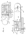
- Referring first to Figures 1 to 5, and 18 to 21, a
mount 10 includes a one-piece mouldedplastic body 11 having recessedopposite ends LED 14. The body defines cavity means such as the two longitudinally extending, laterally spacedcavities opposite ends cavities cavities side 19 of the mount body, adjacent recessedend 13. Acomplementary cavity 18a extends in transverse alignment withcavity 17, but at the opposite side ofcavity 15. Figure 20 shows corresponding structure. - A circuit component with terminals is adapted to be supported by the body, the illustrated component such as
light unit 14 comprising an LED (or other light unit such as an incandescent lamp or Neon lamp).Unit 14 has twoterminals 21 projecting rearwardly from ahousing 22, and also within the latter. Aluminous chip 23 defines the light emitting zone of the LED. A base flange or arcuate boss is shown at 24, and it flatly engages theend wall 13a of the mount, in Figure 4, which surroundsrecess 13. - The
mount 10 also includes contact structure in the body cavity means for removable endwise reception of the terminal means such asterminals 21, to establish electrical contact with same when thebase 24 is supported by the body end portion, in the position of theunit 14 at one end of the body (see Figure 5). See for example thecontact structure 26 illustrated in Figures 12 to 14. It includes acontact body 27 in the form of single electrically conductive, flat (as-stamped) metallic sheet from which laterally spacedspring fingers 28 project longitudinally, in Figure 14. In Figures 12 and 13 thesheet 27 has been rolled into generallycircular arc 27a to locate the three fingers aboutaxis 29, at 120° intervals. Also in Figures 12 and 13 the fingers have been deformed to taper rightwardly so that their narrowedportions 28a define areception zone 30 for aterminal 21, to forcibly grip the latter upon its endwise insertion, as in Figures 4 and 5. These views also show the contact structure inserted into acavity 16.Tabs 31 on the contact structure are received intocavities cavities arcuate section 27a is closely received in the cavity bore to centre the contact structure and the fingers, for axial reception of the terminal. Twosuch contact structures 26 are shown in the twocavities - Auxiliary terminal means 34 also project sidewardly out of the
body 11, and typically closer tobody end 13a than tobody end 12a. The terminal means 34 may be integral with thecontact structure 26, as seen in Figures 12 to 14, and it projects viacavity 18 inbody 11 and an axial slot 80 in the body, to the exterior, for reception by acircuit board 36. A bridge portion of thestamping contacts show board 36 having an opening 36a passing theterminal 34, andsolder 37 anchoring the pin orterminal 34 in the position shown. Sheet solder at side 36b of the board may also be employed. Other circuitry connected toterminal 34 is schematically shown at 39.Ribs 40 onbody side 19 engage the upper side 36b of the board, whereby the mount is ruggedly attached to the board, withlight unit 14 extending parallel thereto. Also, the body is thereby raised from the board to allow tapped flux to be washed away. - In Figure 5, the light unit takes the form of an
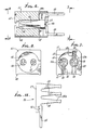
incandescent lamp 140 attached to theopposite end 12a of themount body 11 as shown (of course, any LED or other electrically compound could alternatively be employed, in place of unit 140). Theunit 140 has ahousing 141 with abase 141 aengaging mount end 12a. The twoterminals 142 of theunit 140 project endwise into electrical contact with the grippingspring finger portions 28a. Theends 142a of the terminals may be bent for retaining the terminals and light unit in position i.e. against withdrawal fromcontacts 28a. In similar manner, in Figure 4, theends 21 a ofterminal 21 may be bent for retaining theunit 14 against withdrawal from the spring finger contacts.Wire 143 is adapted to becomes luminous, within glass envelope 144, when electrical current is delivered viaterminals 34 towire 143. - Referring now to. Figures 6 to 10, and 15 to 17, the structure of the
mount body 11 remains the same whereby the mount is "universal" as respect the different contact structure employed, and the different light units or their modes of mounting, at a selected end of the body. Thecontact structure body 27 andfingers 28 also remain the same; however, the terminal 50 (corresponding to terminal 34) projects endwise or longitudinally instead of sidewardly, at one lateral end ofbody 27. Consequently, the twoterminals 50 extends endwise of thebody 11 in Figures 6 to 10. As a further consequence, and as shown in Figure 9 to 10, the light unit and body are enabled to project endwise upright from thecircuit board 36, should that mode of mounting be desired. In Figure 9, the light unit 14 (LED) projects upwardly remotely, from the upper side 36b of theboard 36;contact terminals 50 project through theboard openings 52 to be soldered at 53; andlight unit terminals 21 project throughintermediate board openings 54; and ends 21 a of theterminals 21 may be turned for retention atboard side 36a'. - In Figure 10, the structure is like that shown in Figure 9, except that the
mount 11 andlight unit 14 are at opposite sides of theboard 36. The mounting of thebody 11 to the board is the same as in Figure 9, except thatcontact terminals 50 are cutoff proximate the loci of thesolder connections 53. Thebase 24 of the light unit now is located near or seated on thesolder connections 53, or the ends of theterminals 50 so that the light unit terminals project back throughopenings 54 in the board; and into contact with thespring fingers 28, at the opposite side of the boards. Ends 21 a may be turned, as shown, for retention. - In Figure 11, the structure is the same as in Figure 9, excepting that a spacer 60 is located between the
light unit base 24 andend portion 12 of thebody 11. The spacer extends aboutterminal 21; and it fits into the recess defined by the end ofbody 11, for positioning and retention, theend 21 a of the terminal 21 being typically turned to provide such retention. Note also offsets 80 integral with the contact structures and spacing the body from the base.
Claims (20)
Applications Claiming Priority (2)
| Application Number | Priority Date | Filing Date | Title |
|---|---|---|---|
| US72556585A | 1985-04-22 | 1985-04-22 | |
| US725565 | 1985-04-22 |
Publications (2)
| Publication Number | Publication Date |
|---|---|
| EP0200462A2 true EP0200462A2 (en) | 1986-11-05 |
| EP0200462A3 EP0200462A3 (en) | 1987-10-07 |
Family
ID=24915060
Family Applications (1)
| Application Number | Title | Priority Date | Filing Date |
|---|---|---|---|
| EP86303029A Withdrawn EP0200462A3 (en) | 1985-04-22 | 1986-04-22 | Circuit component mount |
Country Status (1)
| Country | Link |
|---|---|
| EP (1) | EP0200462A3 (en) |
Cited By (2)
| Publication number | Priority date | Publication date | Assignee | Title |
|---|---|---|---|---|
| EP1635431A3 (en) * | 2004-09-13 | 2007-08-01 | BöSha GmbH + Co. KG | Explosionproof two-pin lamp socket and explosionproof luminaire |
| WO2010031373A1 (en) | 2008-09-22 | 2010-03-25 | Osram Opto Semiconductors Gmbh | Housing for an optoelectronic component |
Family Cites Families (3)
| Publication number | Priority date | Publication date | Assignee | Title |
|---|---|---|---|---|
| DE1464176B2 (en) * | 1963-09-21 | 1970-09-17 | Raimund Finsterhölzl, Elektrotechn. Spezialfabrik, 7980 Ravensburg | Socket for electric glass base lamps |
| FR2390032A1 (en) * | 1977-05-03 | 1978-12-01 | Sofec | Lamp socket in vehicle instrument panel - can be removed from display panel without any dismantling of panel using sprung contact leaves |
| DE2918620C2 (en) * | 1979-05-09 | 1985-05-23 | ANT Nachrichtentechnik GmbH, 7150 Backnang | Arrangement of cuboid holders for optoelectronic components |
-
1986
- 1986-04-22 EP EP86303029A patent/EP0200462A3/en not_active Withdrawn
Cited By (4)
| Publication number | Priority date | Publication date | Assignee | Title |
|---|---|---|---|---|
| EP1635431A3 (en) * | 2004-09-13 | 2007-08-01 | BöSha GmbH + Co. KG | Explosionproof two-pin lamp socket and explosionproof luminaire |
| WO2010031373A1 (en) | 2008-09-22 | 2010-03-25 | Osram Opto Semiconductors Gmbh | Housing for an optoelectronic component |
| US8558271B2 (en) | 2008-09-22 | 2013-10-15 | Osram Opto Semiconductors Gmbh | Housing for an optoelectronic component |
| CN102160200B (en) * | 2008-09-22 | 2014-05-28 | 欧司朗光电半导体有限公司 | Housing for an optoelectronic component |
Also Published As
| Publication number | Publication date |
|---|---|
| EP0200462A3 (en) | 1987-10-07 |
Similar Documents
| Publication | Publication Date | Title |
|---|---|---|
| US4727648A (en) | Circuit component mount and assembly | |
| US4837927A (en) | Method of mounting circuit component to a circuit board | |
| KR100385011B1 (en) | Lamp with contact lugs having longitudinal slots for holding electrical contacts of devices in first and second planes | |
| US6712641B2 (en) | Resilient contact and assembly thereof | |
| US5087212A (en) | Socket for light emitting diode | |
| EP0342961A2 (en) | Light-emitting diode assembly | |
| EP0373003A2 (en) | Surface-mounted component's contact having a soldering portion | |
| US6413117B1 (en) | Axisymmetric vibrator, vibrator connection, and mounting system | |
| EP0404135A2 (en) | Wedge base socket attached to SPG substrate | |
| JPH08306413A (en) | Hold mechanism that keeps electric connector to printed-circuit board | |
| US4414298A (en) | Printed circuit board mount for batteries and the like | |
| US5057982A (en) | Indicator lamp | |
| EP0684756A2 (en) | Socket having an auxiliary electrical component mounted thereon | |
| US5807121A (en) | Junction component for connecting the electrical leads of a printed circuit board and a separate electrical unit | |
| KR940001264B1 (en) | Adapter for a single-base low pressure discharge lamp | |
| EP0588395A2 (en) | Electrical assembly and connector therefor | |
| US4410928A (en) | Connector fixing device | |
| EP0109297B1 (en) | Improvements in electrical contact members and electrical connector assemblies | |
| EP0200462A2 (en) | Circuit component mount | |
| EP0194758A1 (en) | Electrical connector for printed circuits | |
| JPS6331339Y2 (en) | ||
| US6008570A (en) | Compact low-pressure discharge lamp with conductive spring element | |
| KR20020041297A (en) | High-voltage connector | |
| EP0929127A1 (en) | Branch junction box assembly | |
| US2253164A (en) | Electrical connector |
Legal Events
| Date | Code | Title | Description |
|---|---|---|---|
| PUAI | Public reference made under article 153(3) epc to a published international application that has entered the european phase |
Free format text: ORIGINAL CODE: 0009012 |
|
| AK | Designated contracting states |
Kind code of ref document: A2 Designated state(s): BE DE FR GB LU NL |
|
| PUAB | Information related to the publication of an a document modified or deleted |
Free format text: ORIGINAL CODE: 0009199EPPU |
|
| RA1 | Application published (corrected) |
Date of ref document: 19861210 Kind code of ref document: A2 |
|
| PUAL | Search report despatched |
Free format text: ORIGINAL CODE: 0009013 |
|
| RHK1 | Main classification (correction) |
Ipc: H01R 33/09 |
|
| AK | Designated contracting states |
Kind code of ref document: A3 Designated state(s): BE DE FR GB LU NL |
|
| 17P | Request for examination filed |
Effective date: 19880402 |
|
| 17Q | First examination report despatched |
Effective date: 19901031 |
|
| STAA | Information on the status of an ep patent application or granted ep patent |
Free format text: STATUS: THE APPLICATION IS DEEMED TO BE WITHDRAWN |
|
| 18D | Application deemed to be withdrawn |
Effective date: 19931006 |