EP0200440B1 - Electronic circuit for connecting a processor to a high-capacity memory - Google Patents
Electronic circuit for connecting a processor to a high-capacity memory Download PDFInfo
- Publication number
- EP0200440B1 EP0200440B1 EP86302947A EP86302947A EP0200440B1 EP 0200440 B1 EP0200440 B1 EP 0200440B1 EP 86302947 A EP86302947 A EP 86302947A EP 86302947 A EP86302947 A EP 86302947A EP 0200440 B1 EP0200440 B1 EP 0200440B1
- Authority
- EP
- European Patent Office
- Prior art keywords
- memory
- processor
- segments
- decoder
- seg
- Prior art date
- Legal status (The legal status is an assumption and is not a legal conclusion. Google has not performed a legal analysis and makes no representation as to the accuracy of the status listed.)
- Expired
Links
Images

Classifications
-
- G—PHYSICS
- G06—COMPUTING OR CALCULATING; COUNTING
- G06F—ELECTRIC DIGITAL DATA PROCESSING
- G06F12/00—Accessing, addressing or allocating within memory systems or architectures
- G06F12/02—Addressing or allocation; Relocation
- G06F12/0223—User address space allocation, e.g. contiguous or non contiguous base addressing
- G06F12/0292—User address space allocation, e.g. contiguous or non contiguous base addressing using tables or multilevel address translation means
Definitions
- the present invention relates to an electronic circuit for connecting a processor to a high-capacity memory in which the processor is provided with an address bus having a given width, for example 16 bits, for addressing the memory.
- the processor can directly address a given number of bytes at a time, for example 64K, but it is desirable for it to be able to address a memory which is larger than this.
- US-A-4 037 215 It is known from US-A-4 037 215 to provide a processor with means for connecting it to a segmented memory, in which the memory segments each have a capacity such that they can be directly addressed by means of a first portion of the address supplied by the processor.
- a translator or auxiliary memory is interposed between the processor and the memory and comprises a plurality of registers, subdivided into groups with each group comprising a number of registers which is equal to the number of memory segments which can be addressed at one time by the processor. In use one of the groups is selected and the registers in the selected group are addressed by a second portion of the address supplied by the processor. The registers identify which of the segments of the processor are to be addressed.
- a different one of the register groups can be selected. Sufficient bits are required to address the selected one of the groups of registers. The information in the registers can also be changed.
- the present invention provides an improved circuit for connecting a processor to a high-capacity memory as defined in claim 1 below.
- Advantageous features are set out in the dependent claims.
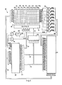
- an electronic circuit 10 embodying the invention provides the connection between a processor 20 and a memory 21 having a high capacity, for example 1 Megabyte.
- the processor 20 may be of any known type but in the embodiment described herein reference will be made to a Zilog Z80 microprocessor which comprises an 8 channel data bus 22 for bi-directional transfer of the 8 bit data (D0-D7), and a 16 channel address bus 23 for addressing the memory 21 and the devices connected thereto, by means of 16 addresses (AO-A15).
- a Zilog Z80 microprocessor which comprises an 8 channel data bus 22 for bi-directional transfer of the 8 bit data (D0-D7), and a 16 channel address bus 23 for addressing the memory 21 and the devices connected thereto, by means of 16 addresses (AO-A15).
- the high-capacity memory 21 ( Figures 1 and 2) is connected to the processor 20 by means of the data bus 22 and is subdivided into 256 segments (SEG 0 - SEG 255), each of which has a capacity of 4 Kbytes.
- the memory 21 can be addressed by twenty address bits MAO-MA19, the 12 least significant of which (MAO-MA11) are connected by means of two portions 24 and 26 of the address bus 23 directly to the 12 least significant address bits (AO-A11 ) of the processor 20.
- the circuit 10 further comprises a random access memory 30 (RAM) formed by 16 registers (RO-R15), each of 8 bits.
- RAM random access memory
- the RAM 30 is associated with a first decoder 31 whose input, by means of a portion 27 of the bus 23, receives the addresses A12, A13, A14 and A15, and whose outputs are capable of enabling the registers RO-R15 one at a time.
- the RAM 30 is also connected to the processor 20 by means of the data bus 22 for receiving the data DO-D7 and is capable of generating eight signals RA12-RA19 which, by means of eight corresponding NAND gates 32, generate the eight most significant address signals MA12-MA19 for the memory 21, to which they are passed by means of a bus 28.
- the circuit 10 further comprises a second decoder 35 which is capable of generating an enabling signal CS for the first decoder 31 and whose input receives the addresses AO-A7 from the processor 20 and a signal WRE which is generated by an AND gate 36.
- the inputs of the AND gate 36 receive from the processor 20 a signal WR which is indicative of the fact that a certain item of data (DO-D7) is to be written or stored in one of the memories, and a signal IORQ which is indicative of the fact that the addresses AO-A7 are intended for an input/output unit for data input or output operations.
- the NAND gates 32 are enabled by a signal RDE generated by a flip-flop 38 which has a set input connected to the output of an AND gate 39 and a reset input connected to a general reset signal RS which is also passed to the processor 20.
- the AND gate 39 receives from the processor 20 the signal IORQ and a signal RD which is indicative of the fact that data are to be read from one of the memories or an input/output unit.
- the flip-flop 38 is reset in such a way as to put the signal RDE at level 0, and consequently all the outputs MA12-MA19 of the gates 32 at level 1.
- the first of the segments (SEG 0) of the memory 21 is addressed, being the segment containing the items of information relating to the number of the other segments, among the total of 256, to be associated with the processor 20 in this first phase.
- the processor 20 reads the items of information stored in the segment SEG 0 and "writes" in each of the registers R00-R15 of the RAM 30 the value of the sixteen memory segments 21 with which it is successively connected. For each cycle in the RAM 30, the signals WR and IORQ are brought to level 1 so that the signal WRE, going to level 1, enables the decoder 35 to generate the signal CS which in turn enables the decoder 31.
- the addresses A12-A15 which are combined together address one at a time the registers RO-R15 in such a way that, when the data DO-D7 arrive from the processor 20, they are stored in the addressed register.
- the signal RDE remains at level 0 and maintains at level 1 the outputs MA12-MA19 of the NAND gates 32.
- the processor 20 When the processor 20 is to perform a cycle of reading the RAM 30, it brings to level 1 the signals RD and IORQ which, by means of the AND gate 39, set the flip-flop 38, sending the signal RDE to level 1. In that way, with the RAM 30 being addressed by means of the addresses A12-A15, the registers RO-R15 are read. The content of the each register RO-R15 comes out of the RAM 30 by means of the eight signals RA12-RA19 and, by way of the NAND gates 32, becomes the address code for one of the 256 segments of the high-capacity memory 21.
- the processor 20 with 16 bit addressing (A0-A15), manages to be connected to each cell of any one of the 16 segments of the memory 21, which were previously selected among the total of 256 segments.
- the processor 20 is capable of changing the content of the registers RO-R15 of the RAM 30, effecting a writing cycle in the manner described hereinbefore, and thus being connected to other segments of the memory 21.
- the processor 20 while being capable of addressing only 64 Kbytes of memory 21 at a time, has the entire 1 Megabyte memory available.
- An electronic circuit of the type described hereinbefore may be used in any data processing or word processing units or in electronic typewriters provided with processors.
Landscapes
- Engineering & Computer Science (AREA)
- Theoretical Computer Science (AREA)
- Physics & Mathematics (AREA)
- General Engineering & Computer Science (AREA)
- General Physics & Mathematics (AREA)
- Microcomputers (AREA)
- Memory System (AREA)
- Multi Processors (AREA)
Description
- The present invention relates to an electronic circuit for connecting a processor to a high-capacity memory in which the processor is provided with an address bus having a given width, for example 16 bits, for addressing the memory. In that way the processor can directly address a given number of bytes at a time, for example 64K, but it is desirable for it to be able to address a memory which is larger than this.
- It is known from US-A-4 037 215 to provide a processor with means for connecting it to a segmented memory, in which the memory segments each have a capacity such that they can be directly addressed by means of a first portion of the address supplied by the processor. A translator or auxiliary memory is interposed between the processor and the memory and comprises a plurality of registers, subdivided into groups with each group comprising a number of registers which is equal to the number of memory segments which can be addressed at one time by the processor. In use one of the groups is selected and the registers in the selected group are addressed by a second portion of the address supplied by the processor. The registers identify which of the segments of the processor are to be addressed.
- To change the segments which are addressed, a different one of the register groups can be selected. Sufficient bits are required to address the selected one of the groups of registers. The information in the registers can also be changed.
- The present invention provides an improved circuit for connecting a processor to a high-capacity memory as defined in
claim 1 below. Advantageous features are set out in the dependent claims. - It is thus not necessary to provide for selection bits to select a group of registers, and the whole of the address output of the processor can be used to address the memory. However, changing (or loading) the content of the registers is possible at any time by performing a simple modification sequence to read information from the predetermined memory segment.
- These and other features of the invention will be clearly apparent from the following description of a preferred embodiment which is given by way of non-limiting example with reference to the accompanying drawings in which:-
- Figure 1 is a block diagram of an electronic circuit embodying the invention, and
- Figure 2 is a block diagram showing the map for addressing of the high-capacity memory of the circuit shown in Figure 1.
- Referring to Figure 1, an
electronic circuit 10 embodying the invention provides the connection between aprocessor 20 and amemory 21 having a high capacity, for example 1 Megabyte. - The
processor 20 may be of any known type but in the embodiment described herein reference will be made to a Zilog Z80 microprocessor which comprises an 8channel data bus 22 for bi-directional transfer of the 8 bit data (D0-D7), and a 16channel address bus 23 for addressing thememory 21 and the devices connected thereto, by means of 16 addresses (AO-A15). - The high-capacity memory 21 (Figures 1 and 2) is connected to the
processor 20 by means of thedata bus 22 and is subdivided into 256 segments (SEG 0 - SEG 255), each of which has a capacity of 4 Kbytes. Thememory 21 can be addressed by twenty address bits MAO-MA19, the 12 least significant of which (MAO-MA11) are connected by means of twoportions address bus 23 directly to the 12 least significant address bits (AO-A11 ) of theprocessor 20. - The
circuit 10 further comprises a random access memory 30 (RAM) formed by 16 registers (RO-R15), each of 8 bits. TheRAM 30 is associated with afirst decoder 31 whose input, by means of aportion 27 of thebus 23, receives the addresses A12, A13, A14 and A15, and whose outputs are capable of enabling the registers RO-R15 one at a time. - The
RAM 30 is also connected to theprocessor 20 by means of thedata bus 22 for receiving the data DO-D7 and is capable of generating eight signals RA12-RA19 which, by means of eightcorresponding NAND gates 32, generate the eight most significant address signals MA12-MA19 for thememory 21, to which they are passed by means of abus 28. - The
circuit 10 further comprises asecond decoder 35 which is capable of generating an enabling signal CS for thefirst decoder 31 and whose input receives the addresses AO-A7 from theprocessor 20 and a signal WRE which is generated by an ANDgate 36. The inputs of the ANDgate 36 receive from the processor 20 a signal WR which is indicative of the fact that a certain item of data (DO-D7) is to be written or stored in one of the memories, and a signal IORQ which is indicative of the fact that the addresses AO-A7 are intended for an input/output unit for data input or output operations. - The
NAND gates 32 are enabled by a signal RDE generated by a flip-flop 38 which has a set input connected to the output of an ANDgate 39 and a reset input connected to a general reset signal RS which is also passed to theprocessor 20. - The AND
gate 39 receives from theprocessor 20 the signal IORQ and a signal RD which is indicative of the fact that data are to be read from one of the memories or an input/output unit. - The mode of operation of the
circuit 10 as described hereinbefore is as follows: - Initially, by means of the reset signal RS, the flip-
flop 38 is reset in such a way as to put the signal RDE atlevel 0, and consequently all the outputs MA12-MA19 of thegates 32 atlevel 1. In that way the first of the segments (SEG 0) of thememory 21 is addressed, being the segment containing the items of information relating to the number of the other segments, among the total of 256, to be associated with theprocessor 20 in this first phase. - The
processor 20 reads the items of information stored in thesegment SEG 0 and "writes" in each of the registers R00-R15 of theRAM 30 the value of the sixteenmemory segments 21 with which it is successively connected. For each cycle in theRAM 30, the signals WR and IORQ are brought tolevel 1 so that the signal WRE, going tolevel 1, enables thedecoder 35 to generate the signal CS which in turn enables thedecoder 31. The addresses A12-A15 which are combined together address one at a time the registers RO-R15 in such a way that, when the data DO-D7 arrive from theprocessor 20, they are stored in the addressed register. - During that writing phase, the signal RDE remains at
level 0 and maintains atlevel 1 the outputs MA12-MA19 of theNAND gates 32. - When the
processor 20 is to perform a cycle of reading theRAM 30, it brings tolevel 1 the signals RD and IORQ which, by means of theAND gate 39, set the flip-flop 38, sending the signal RDE tolevel 1. In that way, with theRAM 30 being addressed by means of the addresses A12-A15, the registers RO-R15 are read. The content of the each register RO-R15 comes out of theRAM 30 by means of the eight signals RA12-RA19 and, by way of theNAND gates 32, becomes the address code for one of the 256 segments of the high-capacity memory 21. - In that way the
processor 20, with 16 bit addressing (A0-A15), manages to be connected to each cell of any one of the 16 segments of thememory 21, which were previously selected among the total of 256 segments. - At any time moreover the
processor 20 is capable of changing the content of the registers RO-R15 of theRAM 30, effecting a writing cycle in the manner described hereinbefore, and thus being connected to other segments of thememory 21. - It will be clear therefore that the
processor 20, while being capable of addressing only 64 Kbytes ofmemory 21 at a time, has the entire 1 Megabyte memory available. - An electronic circuit of the type described hereinbefore may be used in any data processing or word processing units or in electronic typewriters provided with processors.
Claims (5)
Applications Claiming Priority (2)
| Application Number | Priority Date | Filing Date | Title |
|---|---|---|---|
| IT6739685 | 1985-04-30 | ||
| IT67396/85A IT1183808B (en) | 1985-04-30 | 1985-04-30 | ELECTRONIC CIRCUIT TO CONNECT A MICROPROCESSOR TO A HIGH CAPACITY MEMORY |
Publications (3)
| Publication Number | Publication Date |
|---|---|
| EP0200440A2 EP0200440A2 (en) | 1986-11-05 |
| EP0200440A3 EP0200440A3 (en) | 1988-09-28 |
| EP0200440B1 true EP0200440B1 (en) | 1992-07-01 |
Family
ID=11302043
Family Applications (1)
| Application Number | Title | Priority Date | Filing Date |
|---|---|---|---|
| EP86302947A Expired EP0200440B1 (en) | 1985-04-30 | 1986-04-18 | Electronic circuit for connecting a processor to a high-capacity memory |
Country Status (5)
| Country | Link |
|---|---|
| US (1) | US4805092A (en) |
| EP (1) | EP0200440B1 (en) |
| JP (1) | JPH0731626B2 (en) |
| DE (1) | DE3685844T2 (en) |
| IT (1) | IT1183808B (en) |
Families Citing this family (14)
| Publication number | Priority date | Publication date | Assignee | Title |
|---|---|---|---|---|
| IT1184013B (en) * | 1985-12-13 | 1987-10-22 | Elsag | HIGH CAPACITY MEMORY ACCESSIBLE TO DIFFERENT AGENTS |
| JPS63282870A (en) * | 1987-05-14 | 1988-11-18 | Minolta Camera Co Ltd | Address specification system for memory unit |
| IT1216085B (en) * | 1988-03-15 | 1990-02-22 | Honeywell Bull Spa | QUICK LOCAL MEMORY SELECTION APPARATUS. |
| CA2003821C (en) * | 1989-04-20 | 1996-12-03 | Richard J. Molnar | Process controller single memory chip shadowing technique |
| US5210847A (en) * | 1989-05-19 | 1993-05-11 | Compaq Computer Corporation | Noncacheable address random access memory |
| JPH03137744A (en) * | 1989-10-24 | 1991-06-12 | Toshiba Corp | Memory control system |
| US5317706A (en) * | 1989-11-15 | 1994-05-31 | Ncr Corporation | Memory expansion method and apparatus in a virtual memory system |
| US5175835A (en) * | 1990-01-10 | 1992-12-29 | Unisys Corporation | Multi-mode DRAM controller |
| US5255382A (en) * | 1990-09-24 | 1993-10-19 | Pawloski Martin B | Program memory expander for 8051-based microcontrolled system |
| JP3181307B2 (en) * | 1991-04-25 | 2001-07-03 | 株式会社東芝 | Instruction processing unit |
| WO1993022726A1 (en) * | 1992-05-04 | 1993-11-11 | Compaq Computer Corporation | Single map data destination facility |
| US5627986A (en) * | 1992-08-31 | 1997-05-06 | Rockwell International Corporation | Device and method for selecting and addressing extended memory addresses |
| US5341494A (en) * | 1993-02-12 | 1994-08-23 | Compaq Computer Corporation | Memory accessing system with an interface and memory selection unit utilizing write protect and strobe signals |
| US9990282B2 (en) | 2016-04-27 | 2018-06-05 | Oracle International Corporation | Address space expander for a processor |
Family Cites Families (21)
| Publication number | Priority date | Publication date | Assignee | Title |
|---|---|---|---|---|
| US3292151A (en) * | 1962-06-04 | 1966-12-13 | Ibm | Memory expansion |
| US3786436A (en) * | 1973-03-14 | 1974-01-15 | Gte Automatic Electric Lab Inc | Memory expansion arrangement in a central processor |
| US3949378A (en) * | 1974-12-09 | 1976-04-06 | The United States Of America As Represented By The Secretary Of The Navy | Computer memory addressing employing base and index registers |
| JPS5171648A (en) * | 1974-12-18 | 1976-06-21 | Panafacom Ltd | |
| JPS5752664B2 (en) * | 1974-12-27 | 1982-11-09 | ||
| US3976976A (en) * | 1975-04-04 | 1976-08-24 | The United States Of America As Represented By The Secretary Of The Navy | Method and means to access and extended memory unit |
| US4042911A (en) * | 1976-04-30 | 1977-08-16 | International Business Machines Corporation | Outer and asynchronous storage extension system |
| US4037215A (en) * | 1976-04-30 | 1977-07-19 | International Business Machines Corporation | Key controlled address relocation translation system |
| JPS533029A (en) * | 1976-06-30 | 1978-01-12 | Toshiba Corp | Electronic computer |
| US4092715A (en) * | 1976-09-22 | 1978-05-30 | Honeywell Information Systems Inc. | Input-output unit having extended addressing capability |
| US4363091A (en) * | 1978-01-31 | 1982-12-07 | Intel Corporation | Extended address, single and multiple bit microprocessor |
| US4164786A (en) * | 1978-04-11 | 1979-08-14 | The Bendix Corporation | Apparatus for expanding memory size and direct memory addressing capabilities of digital computer means |
| FR2428871A1 (en) * | 1978-06-15 | 1980-01-11 | Philips Data Syst | EXTENDING THE DIRECT ADDRESSING SPACE IN A COMPUTER SYSTEM |
| DE2846054C2 (en) * | 1978-10-23 | 1985-08-14 | Siemens AG, 1000 Berlin und 8000 München | Circuit arrangement for expanding the addressing volume of a central unit, in particular a microprocessor |
| US4419727A (en) * | 1979-01-02 | 1983-12-06 | Honeywell Information Systems Inc. | Hardware for extending microprocessor addressing capability |
| US4346441A (en) * | 1980-04-29 | 1982-08-24 | Honeywell Information Systems Inc. | Random access memory system for extending the memory addressing capacity of a CPU |
| US4443847A (en) * | 1981-02-05 | 1984-04-17 | International Business Machines Corporation | Page addressing mechanism |
| US4473877A (en) * | 1981-04-16 | 1984-09-25 | Tulk Ronald K | Parasitic memory expansion for computers |
| US4503491A (en) * | 1981-06-29 | 1985-03-05 | Matsushita Electric Industrial Co., Ltd. | Computer with expanded addressing capability |
| US4453212A (en) * | 1981-07-13 | 1984-06-05 | Burroughs Corporation | Extended address generating apparatus and method |
| DE3176950D1 (en) * | 1981-08-12 | 1989-01-12 | Ibm | Extended addressing apparatus and method for direct storage access devices |
-
1985
- 1985-04-30 IT IT67396/85A patent/IT1183808B/en active
-
1986
- 1986-04-18 EP EP86302947A patent/EP0200440B1/en not_active Expired
- 1986-04-18 DE DE8686302947T patent/DE3685844T2/en not_active Expired - Lifetime
- 1986-04-28 JP JP61099269A patent/JPH0731626B2/en not_active Expired - Lifetime
- 1986-04-30 US US06/857,340 patent/US4805092A/en not_active Expired - Lifetime
Also Published As
| Publication number | Publication date |
|---|---|
| JPS61271548A (en) | 1986-12-01 |
| DE3685844T2 (en) | 1993-02-18 |
| IT1183808B (en) | 1987-10-22 |
| IT8567396A1 (en) | 1986-10-30 |
| EP0200440A3 (en) | 1988-09-28 |
| EP0200440A2 (en) | 1986-11-05 |
| IT8567396A0 (en) | 1985-04-30 |
| US4805092A (en) | 1989-02-14 |
| DE3685844D1 (en) | 1992-08-06 |
| JPH0731626B2 (en) | 1995-04-10 |
Similar Documents
| Publication | Publication Date | Title |
|---|---|---|
| US4361868A (en) | Device for increasing the length of a logic computer address | |
| EP0285986B1 (en) | Data processing system with means for contiguously addressing memory | |
| EP0200440B1 (en) | Electronic circuit for connecting a processor to a high-capacity memory | |
| EP0473275B1 (en) | Memory control unit and memory unit | |
| US4694394A (en) | Microprocessor system having a multiplexed address/data bus which communicates with a plurality of memory and input/output devices including TTL output gates | |
| US4654787A (en) | Apparatus for locating memory modules having different sizes within a memory space | |
| US5483491A (en) | Memory card device | |
| US4204252A (en) | Writeable control store for use in a data processing system | |
| GB1277902A (en) | Data processing systems | |
| HK18590A (en) | Extended addressing apparatus and method for direct storage access devices | |
| US5765203A (en) | Storage and addressing method for a buffer memory control system for accessing user and error imformation | |
| CA1216955A (en) | Memory paging system in a microcomputer | |
| GB1468783A (en) | Memory systems | |
| US5025368A (en) | Microprocessor with option area adjacent CPU core facilitating interfacing with peripheral devices | |
| US4156290A (en) | Speedup addressing device by detecting repetitive addressing | |
| US4679167A (en) | Apparatus for locating a memory module within a memory space | |
| JPS6237421B2 (en) | ||
| DE3473520D1 (en) | Circuit arrangement comprising a memory and an access control unit | |
| US4099256A (en) | Method and apparatus for establishing, reading, and rapidly clearing a translation table memory | |
| US3525081A (en) | Auxiliary store access control for a data processing system | |
| EP0057815B1 (en) | Page addressing mechanism and method for using the same | |
| US4249250A (en) | Computer storage arrangements with overwrite warning | |
| US4125879A (en) | Double ended stack computer store | |
| JPH0792734B2 (en) | Memory device | |
| SU1203527A1 (en) | Device for generating data address |
Legal Events
| Date | Code | Title | Description |
|---|---|---|---|
| PUAI | Public reference made under article 153(3) epc to a published international application that has entered the european phase |
Free format text: ORIGINAL CODE: 0009012 |
|
| AK | Designated contracting states |
Kind code of ref document: A2 Designated state(s): DE FR GB |
|
| PUAL | Search report despatched |
Free format text: ORIGINAL CODE: 0009013 |
|
| AK | Designated contracting states |
Kind code of ref document: A3 Designated state(s): DE FR GB |
|
| 17P | Request for examination filed |
Effective date: 19890309 |
|
| 17Q | First examination report despatched |
Effective date: 19901130 |
|
| GRAA | (expected) grant |
Free format text: ORIGINAL CODE: 0009210 |
|
| AK | Designated contracting states |
Kind code of ref document: B1 Designated state(s): DE FR GB |
|
| REF | Corresponds to: |
Ref document number: 3685844 Country of ref document: DE Date of ref document: 19920806 |
|
| ET | Fr: translation filed | ||
| PLBE | No opposition filed within time limit |
Free format text: ORIGINAL CODE: 0009261 |
|
| STAA | Information on the status of an ep patent application or granted ep patent |
Free format text: STATUS: NO OPPOSITION FILED WITHIN TIME LIMIT |
|
| 26N | No opposition filed | ||
| REG | Reference to a national code |
Ref country code: GB Ref legal event code: IF02 |
|
| PGFP | Annual fee paid to national office [announced via postgrant information from national office to epo] |
Ref country code: FR Payment date: 20050408 Year of fee payment: 20 |
|
| PGFP | Annual fee paid to national office [announced via postgrant information from national office to epo] |
Ref country code: GB Payment date: 20050413 Year of fee payment: 20 |
|
| PGFP | Annual fee paid to national office [announced via postgrant information from national office to epo] |
Ref country code: DE Payment date: 20050414 Year of fee payment: 20 |
|
| PG25 | Lapsed in a contracting state [announced via postgrant information from national office to epo] |
Ref country code: GB Free format text: LAPSE BECAUSE OF EXPIRATION OF PROTECTION Effective date: 20060417 |
|
| REG | Reference to a national code |
Ref country code: GB Ref legal event code: PE20 |