EP0200342A2 - Verfahren zur Auswertung der oberflächlichen und unteroberflächlichen Kennzeichen einer Probe - Google Patents
Verfahren zur Auswertung der oberflächlichen und unteroberflächlichen Kennzeichen einer Probe Download PDFInfo
- Publication number
- EP0200342A2 EP0200342A2 EP86302119A EP86302119A EP0200342A2 EP 0200342 A2 EP0200342 A2 EP 0200342A2 EP 86302119 A EP86302119 A EP 86302119A EP 86302119 A EP86302119 A EP 86302119A EP 0200342 A2 EP0200342 A2 EP 0200342A2
- Authority
- EP
- European Patent Office
- Prior art keywords
- sample
- probe beam
- recited
- thermal
- probe
- Prior art date
- Legal status (The legal status is an assumption and is not a legal conclusion. Google has not performed a legal analysis and makes no representation as to the accuracy of the status listed.)
- Withdrawn
Links
Images
Classifications
-
- G—PHYSICS
- G01—MEASURING; TESTING
- G01N—INVESTIGATING OR ANALYSING MATERIALS BY DETERMINING THEIR CHEMICAL OR PHYSICAL PROPERTIES
- G01N25/00—Investigating or analyzing materials by the use of thermal means
- G01N25/72—Investigating presence of flaws
-
- G—PHYSICS
- G01—MEASURING; TESTING
- G01N—INVESTIGATING OR ANALYSING MATERIALS BY DETERMINING THEIR CHEMICAL OR PHYSICAL PROPERTIES
- G01N21/00—Investigating or analysing materials by the use of optical means, i.e. using sub-millimetre waves, infrared, visible or ultraviolet light
- G01N21/17—Systems in which incident light is modified in accordance with the properties of the material investigated
- G01N21/47—Scattering, i.e. diffuse reflection
-
- G—PHYSICS
- G01—MEASURING; TESTING
- G01N—INVESTIGATING OR ANALYSING MATERIALS BY DETERMINING THEIR CHEMICAL OR PHYSICAL PROPERTIES
- G01N21/00—Investigating or analysing materials by the use of optical means, i.e. using sub-millimetre waves, infrared, visible or ultraviolet light
- G01N21/17—Systems in which incident light is modified in accordance with the properties of the material investigated
- G01N2021/178—Methods for obtaining spatial resolution of the property being measured
- G01N2021/1782—In-depth resolution
-
- G—PHYSICS
- G01—MEASURING; TESTING
- G01N—INVESTIGATING OR ANALYSING MATERIALS BY DETERMINING THEIR CHEMICAL OR PHYSICAL PROPERTIES
- G01N21/00—Investigating or analysing materials by the use of optical means, i.e. using sub-millimetre waves, infrared, visible or ultraviolet light
- G01N21/84—Systems specially adapted for particular applications
- G01N2021/8461—Investigating impurities in semiconductor, e.g. Silicon
-
- G—PHYSICS
- G01—MEASURING; TESTING
- G01N—INVESTIGATING OR ANALYSING MATERIALS BY DETERMINING THEIR CHEMICAL OR PHYSICAL PROPERTIES
- G01N21/00—Investigating or analysing materials by the use of optical means, i.e. using sub-millimetre waves, infrared, visible or ultraviolet light
- G01N21/17—Systems in which incident light is modified in accordance with the properties of the material investigated
- G01N21/171—Systems in which incident light is modified in accordance with the properties of the material investigated with calorimetric detection, e.g. with thermal lens detection
Definitions
- the present invention relates to a method and apparatus for evaluating surface and subsurface characteristics of a sample.
- a beam of energy In a thermal wave system, a beam of energy, usually a laser or an electron beam, is focused and scanned across the surface of the sample.
- the beam is intensity modulated at a frequency in the 10 Hz to 10 MHz range.
- This periodic heating is the source of thermal waves that propagate from the heated region.
- the thermal waves are diffusive waves similar to eddy current waves, evanescent waves and other critically damped phenomena that travel only one or two wavelengths before their intensity becomes negligibly small. Nevertheless, within their range, the thermal waves interact with thermal features in a manner that is mathematically equivalent to scattering and reflection processes of conventional propagating waves. Thus, any features on or beneath the surface of the sample that are within the range of these thermal waves and that possess thermal characteristics different from their surroundings will reflect and scatter the thermal waves and thus become visible.
- thermal wave imaging also offers the opportunity for nondestructive depth profiling and determination of thin film layer thicknesses.
- the first approach included the measurement of acoustic wave carriers that are generated by the thermal waves. This approach was described in U.S. Patent 4,255,971, issued March 17, 1981, to Rosencwaig.
- the above described technique while accurate, is a "contact" technique, which requires the connection of a piezoelectric transducer to the sample.
- a radiation probe is directed within the periodically excited area on the surface of the sample in a manner to be specularly reflected.
- This probe beam will undergo periodic angular displacements because of the periodic local angular changes in the surface conditions of the sample induced by the presence of the thermal waves.
- These periodic angular displacements can be detected, using a split or bicell photodetector. This approach is described in European Patent Application No. 8330 4271.6, Publication No. 0102730.
- Another noncontact technique includes the detection of changes in the reflectivity of a probe beam. More specifically, the index of refraction of a sample will vary as the sample is periodically heated. Accordingly, if a probe beam is reflected off the surface of the sample, a reflected probe beam will vary in intensity in a manner corresponding to the changes in the index of refraction of the surface of the sample. Since the changing index of refraction is a function of the changes in the surface temperature induced by the thermal waves, by detecting changes in the intensity of the probe beam, the thermal waves can be detected.
- a device for detecting thermal waves based on the changes in optical reflectivity is described in European Patent Application No. 8530 3511.1, Publication No. 0165711.
- the plasma density at the surface of the sample will vary based on the sample characteristics. Furthermore, the variations in plasma density will affect the refractive index at the surface of the sample.
- the changing refractive index can be measured utilizing some of the noncontact techniques which have previously been successful in the measurement of thermal waves. More specifically, a radiation probe can be reflected off the surface of the sample and changes induced in the radiation probe by the plasma induced changes in the refractive index can be monitored to obtain information about surface and subsurface characteristics of the sample.
- Plasma density analysis can be used to evaluate ion dopant characteristics and other features which vary across the sample and also as a function of depth beneath the sample surface.
- An apparatus for detecting plasma density variations is described in European Patent Application No. 8630 1289.4.
- the alternate technique would also be of the noncontact variety to permit evaluation in a manufacturing situation.
- the subject invention provides for a new and improved method and apparatus for evaluating surface and subsurface conditions of a sample.
- the subject invention is particularly suited for detecting thermal and/or plasma waves in a sample.
- the present invention relates to a new and improved method and apparatus for evaluating surface and subsurface features in a sample by detecting scattering of a probe beam. More particularly, the subject invention relates to the detection of thermal and/or plasma waves through the phenomenon of optical scattering.
- the apparatus includes a periodic excitation source for supplying energy to the surface of the sample to generate either thermal and/or plasma waves.
- a radiation probe is directed to the surface of the sample within the area that is being periodically excited and in a manner that the probe beam is scattered from the excited area. Variations of the intensity of the scattered probe beam are detected and processed to evaluate surface and subsurface characteristics of the sample.
- the apparatus includes a periodic excitation source for supplying energy to the surface of the sample to generate thermal waves and/or plasma density variations.
- a radiation probe beam is provided which is directed to the surface of the sample within the area that it is being periodically excited by the energy source.
- a detector is provided for measuring intensity changes of the radiation probe due to optical scattering of the probe beam from the periodically excited region on the surface of the sample.
- a means is provided for processing the measured intensity changes to evaluate the sample.
- the processing means functions to isolate the intensity changes which are a function of the periodic excitation. The mode of processing will be dependent, in part, upon whether thermal and/or plasma waves are being detected.
- the subject invention is particularly suited for measurement situations where the surface of the sample is a highly scattering medium. For example, if the sample has a rough surface, it can be difficult to arrange optical components in a manner to obtain good measurements of a specularly reflected probe beam.
- the subject technique is also suitable where the sample is nonplanar such that it would be difficult to locate the optical components near the surface of the sample.
- the location of the specularly reflected beam can vary. This effect is increased when the optics are moved farther from the surface of the sample. Where the optics must be moved away from the sample surface, it becomes increasingly difficult to obtain measurements of a specularly reflected probe beam.
- the subject invention can be used without focusing and permits the placement of the detector a significant distance from the sample surface.
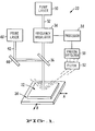
- FIG. 1 there is illustrated an apparatus 20 for performing the method of the subject invention.
- a sample 22 is placed on a movable stage 24.
- the stage is capable of being rastered in two dimensions, as indicated by arrows A and B.
- Such movable stages are well-known in the prior art. It should be noted, however, that the sample could also be kept stationary, and the pump and probe beams scanned across the sample using appropriate optical deflection techniques.
- a means for periodically exciting the sample.
- the means is provided by a laser 30.
- Laser 30 may be an argon-ion laser.
- the energy source or pump can also be provided from any suitable electromagnetic radiation or a particle beam, such as an electron beam. The energy of the beam must be sufficient to generate the thermal waves and/or plasma density variations of interest.
- Laser 30 emits a beam 32 which is passed through a frequency modulator 34.
- the frequency modulator is intended to periodically chop or intensity modulate the beam at a frequency which is variable and under control of the processor 36.
- Beam 32 then passes through a dichroic mirror 36 to the surface of the sample.
- Dichroic mirror 30' is designed to pass the wavelengths of light emitted by the argon ion laser 30 and reflect the light of probe laser 40, as discussed below.
- Beam 32 is directed to the surface of the sample in a manner to periodically excite the sample at its surface.
- the periodic energy beam will function to create thermal waves having a frequency corresponding to the frequency of modulator 34. These thermal waves, while critically damped, will travel one to two wavelengths before becoming too weak to detect.
- the distance which the waves travel in the sample is given by the following equation: where u is the thermal diffusion length, K is the thermal conductivity, P is the density, C is the specific heat, and ⁇ is the modulation frequency of the beam.
- the energy beam can produce an electron-hole plasma.
- An electron-hole plasma will be created if the energy of the beam is sufficient to raise electrons from the valence band to the conduction band, thereby creating electron hole pairs.
- thermal waves may also be produced.
- the energy exceeds the band gap energy electrons which have been excited above the conduction band will, in a relatively short period of time (tau [T] is approximatley equal to 10 -13 seconds) give up a portion of their energy to the lattice through nonradiative transitions to the unoccupied states near the bottom of the conduction band.
- Equations which set forth the diffusion length of the periodic plasma density variations are set forth below. More specifically, in a situation where the decay time tau ( T ) (the time it takes for the electron hole pairs to recombine) is relatively short compared to the modulation period 1/ ⁇ , where ⁇ is the modulation frequency in radian/second (i.e., ⁇ is less than one) then the diffusion length of the plasma is given by the following equation: where D is the diffusivity of the plasma. Note that in this situation plasma waves will not be generated. However, changes in plasma density can still be detected and used to derive information about the sample.
- the above equations which define the diffusion lengths are provided in order to define the area of the sample which is being "periodically excited.” More specifically, and as discussed below, in order to detect the thermal waves and/or plasma density variations, the beam 42 from probe laser 40 must be directed within the periodically excited area on the surface of the sample.
- This periodically excited area can be defined in terms of an excited diameter "D" by the following equation: where the spot radius R is defined by the radius of the modulated energy beam.
- the second term of the equation, diffusion length is given by one of the formulas (1-3) set forth above and will depend on the particular measurement situation. Specifically, where only thermal waves are being measured, the thermal diffusion length u is set forth in equation (1). Similarly, the plasma wave diffusion length equations can be substituted in the proper circumstances. If both thermal and plasma waves are prsent, the exicted area will be defined as the largest of the calculated regions.
- the subject invention further includes a radiation probe 40 which can be defined by an optical beam.
- the radiation probe should emit a beam which is capable of optical scattering.
- probe 40 is defined by a helium-neon laser.
- Beam 42 is deflected by a mirror 44 and onto dichroic mirror 36.
- the dichroic mirror is optically reflective to the wavelengths emitted by probe laser 40.
- the probe laser beam is directed to be coincident with the pump laser beam 32.
- the probe laser beam be directed within the periodically excited region which emanates from the modulated heating beam 32 and extends a distance as defined by equation (4). Note that where the diffusion length is very short, the periodically excited region will be essentially coincident with the periodic energy beam.
- the probe beam will be specularly reflected from the surface of the sample. In addition, portions of the beam will also be scattered. Scattering of a probe beam will generally take place whether or not the energy beam is impinged on the sample. Thus, there will generally be a constant or DC scattering signal which is dependent upon the strength of the probe laser and on the local scattering characteristics of the sample surface. As discussed below, when a periodic excitation source 30 is directed on the surface of the sample, a periodic scattering phenomenon will also occur that is a function of the thermal waves and/or plasma density variations on the surface of the sample.
- the scattering of the probe beam may be detected by a photon detector 50.
- the photon detector 50 can be, for example, a photodetector or photomultiplier tube.
- a filter 52 is provided in front of the input of the detector 50 which allows optical energy from the probe laser to pass, but shields the detector from any radiation from the pump laser beam 32.
- a detector 50 which is adapted to detect impacting photons, will measure both the "DC" scattering and the periodic scattering induced by the presence of thermal and/or plasma waves.
- 1/S o (dS/dn) represents the complex refractive coefficient for scattering.
- Thermal waves can also affect the local geometry of the sample surface. Specifically, the roughness of the surface that produces the DC scattering may also be modulated to some extent by the local thermoelastic expansion of the sample from the thermal waves. This geometric modulation of the sample surface roughness may also contribute to the AC scattering signal. Such an effect has not been observed with plasma waves.
- the output signal generated by detector 50 will include both this DC scattering and the frequency dependent variations in intensity.
- S the amount of DC scattering, into the photon detector, will vary as the local DC scattering characteristics vary.
- the AC signal will also vary as o
- the signal is normalized. More specifically, the signal of interest is examined by normalizing out any output signals from the detector which are not synchronous with the excitation modulation frequency or any of its harmonics.
- One method of deriving the desired signals is to divide the DC signal into the detected signal. The normalized output gives a measure of the thermal or plasma wave activity in a sample.
- the normalized output signal can then be analyzed in a manner described in any of the above patents or applications to derive information about the sample. For example, the signal may be compared to a previously recorded signal of a known sample. Variations between the predetermined signal and the measured signal will indicate variations in the composition of the material. Where dopant concentrations are to be measured, variations in the signal as the probe and energy beam are scanned across the sample surface will give a measure of the varying dopant concentrations mapped out in a two-dimensional image.
- the apparatus includes a periodic excitation source for generating thermal and/or plasma waves in a sample.
- a radiation probe is directed to the surface of the sample within the area which has been periodically excited.
- a means is provided for measuring a portion of the probe beam which has been optically scattered.
- a means is provided for processing the output signals corresponding to the intensity changes of the scattered probe beam that are a function of the periodic variations.
Landscapes
- Physics & Mathematics (AREA)
- Health & Medical Sciences (AREA)
- Life Sciences & Earth Sciences (AREA)
- Chemical & Material Sciences (AREA)
- Analytical Chemistry (AREA)
- Biochemistry (AREA)
- General Health & Medical Sciences (AREA)
- General Physics & Mathematics (AREA)
- Immunology (AREA)
- Pathology (AREA)
- Investigating Or Analysing Materials By Optical Means (AREA)
- Investigating Or Analyzing Materials By The Use Of Ultrasonic Waves (AREA)
- Analysing Materials By The Use Of Radiation (AREA)
- Investigating Materials By The Use Of Optical Means Adapted For Particular Applications (AREA)
Applications Claiming Priority (2)
| Application Number | Priority Date | Filing Date | Title |
|---|---|---|---|
| US06/728,759 US4632561A (en) | 1985-04-30 | 1985-04-30 | Evaluation of surface and subsurface characteristics of a sample |
| US728759 | 1985-04-30 |
Publications (2)
| Publication Number | Publication Date |
|---|---|
| EP0200342A2 true EP0200342A2 (de) | 1986-11-05 |
| EP0200342A3 EP0200342A3 (de) | 1987-08-19 |
Family
ID=24928181
Family Applications (1)
| Application Number | Title | Priority Date | Filing Date |
|---|---|---|---|
| EP86302119A Withdrawn EP0200342A3 (de) | 1985-04-30 | 1986-03-21 | Verfahren zur Auswertung der oberflächlichen und unteroberflächlichen Kennzeichen einer Probe |
Country Status (3)
| Country | Link |
|---|---|
| US (1) | US4632561A (de) |
| EP (1) | EP0200342A3 (de) |
| JP (1) | JPS62251640A (de) |
Cited By (2)
| Publication number | Priority date | Publication date | Assignee | Title |
|---|---|---|---|---|
| EP0239408A3 (de) * | 1986-03-28 | 1989-06-21 | Therma-Wave Inc. | Verfahren und Vorrichtung zur optischen Erfassung von Oberflächenzuständen in Stoffen |
| FR2661754A1 (fr) * | 1990-05-03 | 1991-11-08 | Brunner Thomas | Principe et systeme de l'imagerie optique de hautes resolutions a effet corpusculaire du photon et effet spatio-temporel. |
Families Citing this family (50)
| Publication number | Priority date | Publication date | Assignee | Title |
|---|---|---|---|---|
| FR2593917B1 (fr) * | 1986-02-06 | 1988-06-03 | Univ Reims Champagne Ardenne | Procede et dispositif d'analyse et de mesure des parametres physiques d'un materiau en couches par radiometrie thermique |
| JP2685482B2 (ja) * | 1988-04-08 | 1997-12-03 | 株式会社日立製作所 | 粒子状物質の分析方法及び装置 |
| US4921348A (en) * | 1989-01-26 | 1990-05-01 | Iowa State University Research Foundation, Inc. | Method and means for a spatial and temporal probe for laser-generated plumes based on density gradients |
| US5015950A (en) * | 1989-07-21 | 1991-05-14 | Iowa State University Research Foundation, Inc. | Method and apparatus for determining thermal resistance and structural integrity of coatings on conducting materials by monitoring electrical conductance of the underlying material upon localized heating of the overlying coating |
| US5019775A (en) * | 1989-07-21 | 1991-05-28 | Iowa State University Research Foundation, Inc. | Calibrating an eddy-current-probe using a modulated thermal energy source |
| US5361638A (en) * | 1990-03-30 | 1994-11-08 | Stfi | Arrangement for measuring mechanical properties of a foil material through use of an excitation unit that includes a laser |
| US5196906A (en) * | 1990-06-29 | 1993-03-23 | Tma Technologies, Inc. | Modular scatterometer with interchangeable scanning heads |
| US5270546A (en) * | 1992-04-29 | 1993-12-14 | Mpb Technologies Inc. | Method and apparatus for non-contact, rapid and continuous moisture measurements |
| FR2714970B1 (fr) * | 1994-01-12 | 1996-03-29 | Centre Nat Rech Scient | Ellipsomètre spectroscopique modulé. |
| US5657754A (en) * | 1995-07-10 | 1997-08-19 | Rosencwaig; Allan | Apparatus for non-invasive analyses of biological compounds |
| US5706094A (en) * | 1995-08-25 | 1998-01-06 | Brown University Research Foundation | Ultrafast optical technique for the characterization of altered materials |
| US6008906A (en) | 1995-08-25 | 1999-12-28 | Brown University Research Foundation | Optical method for the characterization of the electrical properties of semiconductors and insulating films |
| US6321601B1 (en) | 1996-08-06 | 2001-11-27 | Brown University Research Foundation | Optical method for the characterization of laterally-patterned samples in integrated circuits |
| US5748318A (en) * | 1996-01-23 | 1998-05-05 | Brown University Research Foundation | Optical stress generator and detector |
| US6175416B1 (en) | 1996-08-06 | 2001-01-16 | Brown University Research Foundation | Optical stress generator and detector |
| US5709471A (en) * | 1996-02-29 | 1998-01-20 | The Aerospace Corporation | Method for thermally testing with a laser the edge of a sapphire window |
| US5844684A (en) * | 1997-02-28 | 1998-12-01 | Brown University Research Foundation | Optical method for determining the mechanical properties of a material |
| US5748317A (en) * | 1997-01-21 | 1998-05-05 | Brown University Research Foundation | Apparatus and method for characterizing thin film and interfaces using an optical heat generator and detector |
| US5978074A (en) * | 1997-07-03 | 1999-11-02 | Therma-Wave, Inc. | Apparatus for evaluating metalized layers on semiconductors |
| US5864393A (en) * | 1997-07-30 | 1999-01-26 | Brown University Research Foundation | Optical method for the determination of stress in thin films |
| US6054868A (en) * | 1998-06-10 | 2000-04-25 | Boxer Cross Incorporated | Apparatus and method for measuring a property of a layer in a multilayered structure |
| US6049220A (en) * | 1998-06-10 | 2000-04-11 | Boxer Cross Incorporated | Apparatus and method for evaluating a wafer of semiconductor material |
| US6885444B2 (en) * | 1998-06-10 | 2005-04-26 | Boxer Cross Inc | Evaluating a multi-layered structure for voids |
| US6038026A (en) | 1998-07-07 | 2000-03-14 | Brown University Research Foundation | Apparatus and method for the determination of grain size in thin films |
| US6025918A (en) * | 1998-07-07 | 2000-02-15 | Brown University Research Foundation | Apparatus and method for measurement of the mechanical properties and electromigration of thin films |
| DE19837889C1 (de) * | 1998-08-20 | 2000-12-21 | Siemens Ag | Thermowellen-Meßverfahren |
| US6323951B1 (en) * | 1999-03-22 | 2001-11-27 | Boxer Cross Incorporated | Apparatus and method for determining the active dopant profile in a semiconductor wafer |
| GB9924425D0 (en) * | 1999-10-16 | 1999-12-15 | British Aerospace | Material analysis |
| US6317216B1 (en) | 1999-12-13 | 2001-11-13 | Brown University Research Foundation | Optical method for the determination of grain orientation in films |
| KR100611109B1 (ko) * | 2000-01-14 | 2006-08-09 | 삼성전자주식회사 | 반도체 장치의 콘택홀 검사 방법 |
| GB0001181D0 (en) * | 2000-01-20 | 2000-03-08 | British Aerospace | Material analysis |
| US6812047B1 (en) * | 2000-03-08 | 2004-11-02 | Boxer Cross, Inc. | Evaluating a geometric or material property of a multilayered structure |
| US6381019B1 (en) * | 2000-06-30 | 2002-04-30 | Brown University Research Foundation | Ultrasonic generator and detector using an optical mask having a grating for launching a plurality of spatially distributed, time varying strain pulses in a sample |
| US6517236B2 (en) * | 2001-02-15 | 2003-02-11 | The University Of Chicago | Method and apparatus for automated thermal imaging of combustor liners and other products |
| US6911349B2 (en) * | 2001-02-16 | 2005-06-28 | Boxer Cross Inc. | Evaluating sidewall coverage in a semiconductor wafer |
| US6812717B2 (en) * | 2001-03-05 | 2004-11-02 | Boxer Cross, Inc | Use of a coefficient of a power curve to evaluate a semiconductor wafer |
| DE10119599A1 (de) * | 2001-04-21 | 2002-10-31 | Bosch Gmbh Robert | Verfahren zur Bestimmung von Temperaturen an Halbleiterbauelementen |
| US6940592B2 (en) * | 2001-10-09 | 2005-09-06 | Applied Materials, Inc. | Calibration as well as measurement on the same workpiece during fabrication |
| US6971791B2 (en) * | 2002-03-01 | 2005-12-06 | Boxer Cross, Inc | Identifying defects in a conductive structure of a wafer, based on heat transfer therethrough |
| US6958814B2 (en) * | 2002-03-01 | 2005-10-25 | Applied Materials, Inc. | Apparatus and method for measuring a property of a layer in a multilayered structure |
| US6963393B2 (en) * | 2002-09-23 | 2005-11-08 | Applied Materials, Inc. | Measurement of lateral diffusion of diffused layers |
| US6878559B2 (en) * | 2002-09-23 | 2005-04-12 | Applied Materials, Inc. | Measurement of lateral diffusion of diffused layers |
| US6888632B2 (en) * | 2003-02-28 | 2005-05-03 | Therma-Wave, Inc. | Modulated scatterometry |
| US6822472B1 (en) * | 2003-06-27 | 2004-11-23 | International Business Machines Corporation | Detection of hard mask remaining on a surface of an insulating layer |
| US7026175B2 (en) * | 2004-03-29 | 2006-04-11 | Applied Materials, Inc. | High throughput measurement of via defects in interconnects |
| WO2006002150A1 (en) * | 2004-06-22 | 2006-01-05 | Applied Materials Israel, Ltd. | Wafer inspection system |
| US7379185B2 (en) | 2004-11-01 | 2008-05-27 | Applied Materials, Inc. | Evaluation of openings in a dielectric layer |
| US7679029B2 (en) * | 2005-10-28 | 2010-03-16 | Cymer, Inc. | Systems and methods to shape laser light as a line beam for interaction with a substrate having surface variations |
| DE102008032555B3 (de) * | 2008-07-10 | 2010-01-21 | Innolas Systems Gmbh | Strukturierungsvorrichtung für die Strukturierung von plattenförmigen Elementen, insbesondere von Dünnschicht-Solarmodulen, entsprechendes Strukturierungsverfahren sowie Verwendung derselben |
| EP3108205B1 (de) * | 2014-02-18 | 2022-08-10 | Novelis, Inc. | Photoakustische vorrichtung und verfahren zur berührungslosen messung von dünnschichten |
Family Cites Families (8)
| Publication number | Priority date | Publication date | Assignee | Title |
|---|---|---|---|---|
| US4243329A (en) * | 1977-11-01 | 1981-01-06 | Citizen Watch Co., Ltd. | Watch movement construction |
| US4255971A (en) * | 1978-11-01 | 1981-03-17 | Allan Rosencwaig | Thermoacoustic microscopy |
| US4243327A (en) * | 1979-01-31 | 1981-01-06 | Nasa | Double-beam optical method and apparatus for measuring thermal diffusivity and other molecular dynamic processes in utilizing the transient thermal lens effect |
| US4284356A (en) * | 1979-09-26 | 1981-08-18 | Ppg Industries, Inc. | Method of and apparatus for comparing surface reflectivity |
| US4513384A (en) * | 1982-06-18 | 1985-04-23 | Therma-Wave, Inc. | Thin film thickness measurements and depth profiling utilizing a thermal wave detection system |
| US4522510A (en) * | 1982-07-26 | 1985-06-11 | Therma-Wave, Inc. | Thin film thickness measurement with thermal waves |
| US4521118A (en) * | 1982-07-26 | 1985-06-04 | Therma-Wave, Inc. | Method for detection of thermal waves with a laser probe |
| US4579463A (en) * | 1984-05-21 | 1986-04-01 | Therma-Wave Partners | Detecting thermal waves to evaluate thermal parameters |
-
1985
- 1985-04-30 US US06/728,759 patent/US4632561A/en not_active Expired - Lifetime
-
1986
- 1986-03-21 EP EP86302119A patent/EP0200342A3/de not_active Withdrawn
- 1986-04-25 JP JP61094973A patent/JPS62251640A/ja active Pending
Cited By (2)
| Publication number | Priority date | Publication date | Assignee | Title |
|---|---|---|---|---|
| EP0239408A3 (de) * | 1986-03-28 | 1989-06-21 | Therma-Wave Inc. | Verfahren und Vorrichtung zur optischen Erfassung von Oberflächenzuständen in Stoffen |
| FR2661754A1 (fr) * | 1990-05-03 | 1991-11-08 | Brunner Thomas | Principe et systeme de l'imagerie optique de hautes resolutions a effet corpusculaire du photon et effet spatio-temporel. |
Also Published As
| Publication number | Publication date |
|---|---|
| US4632561A (en) | 1986-12-30 |
| JPS62251640A (ja) | 1987-11-02 |
| EP0200342A3 (de) | 1987-08-19 |
Similar Documents
| Publication | Publication Date | Title |
|---|---|---|
| US4632561A (en) | Evaluation of surface and subsurface characteristics of a sample | |
| EP0165711B1 (de) | Verfahren und Vorrichtung zum Nachweis von thermischen Wellen | |
| EP0163466B1 (de) | Verfahren und Vorrichtung zur Messung der Dicke und Zusammensetzungen einer geschichteten oder dünnschichtigen Probe | |
| US4634290A (en) | Method and apparatus for detecting thermal waves | |
| EP0200301A1 (de) | Verfahren und Vorrichtung zum Auswerten von Eigenschaften der Oberfläche und des Inneren eines Halbleiters | |
| CA2471334C (en) | Methods for determining the depth of defects | |
| US4513384A (en) | Thin film thickness measurements and depth profiling utilizing a thermal wave detection system | |
| EP0102730B1 (de) | Verfahren zur Detektion thermischer Wellen in einem Prüfling | |
| US8622612B2 (en) | Method and apparatus for determining the thermal expansion of a material | |
| US5042952A (en) | Method and apparatus for evaluating surface and subsurface and subsurface features in a semiconductor | |
| US6183126B1 (en) | Method for nondestructive/noncontact microwave detection of electrical and magnetic property discontinuities in materials | |
| US4952063A (en) | Method and apparatus for evaluating surface and subsurface features in a semiconductor | |
| US5228776A (en) | Apparatus for evaluating thermal and electrical characteristics in a sample | |
| JP4653723B2 (ja) | 光応力発生器及び検出器 | |
| EP0239408A2 (de) | Verfahren und Vorrichtung zur optischen Erfassung von Oberflächenzuständen in Stoffen | |
| JPS6239705B2 (de) | ||
| US6393915B1 (en) | Method and device for simultaneously measuring multiple properties of multilayer films | |
| Bashkansky et al. | Subsurface defect detection in ceramics using an optical gated scatter reflectometer | |
| JPS6234040A (ja) | サンプルの表面および表面下の特性の評価 | |
| JP4932708B2 (ja) | 屈折媒体内に存在するナノ物体の光学的検出方法とシステム | |
| JP3674738B2 (ja) | 少数キャリアのライフタイム測定装置 | |
| Liezers | Thermal Wave Imaging for Nondestructive Testing | |
| US20040246485A1 (en) | Far-field measurement of properties of metallic thin films | |
| Glazov et al. | irradiated semiconductors by photothermal microscopy | |
| Kohlgraf-Owens et al. | Sub-Surface Interferometric Near-Field Tomography |
Legal Events
| Date | Code | Title | Description |
|---|---|---|---|
| PUAI | Public reference made under article 153(3) epc to a published international application that has entered the european phase |
Free format text: ORIGINAL CODE: 0009012 |
|
| AK | Designated contracting states |
Kind code of ref document: A2 Designated state(s): DE FR GB NL |
|
| PUAL | Search report despatched |
Free format text: ORIGINAL CODE: 0009013 |
|
| AK | Designated contracting states |
Kind code of ref document: A3 Designated state(s): DE FR GB NL |
|
| 17P | Request for examination filed |
Effective date: 19880217 |
|
| 17Q | First examination report despatched |
Effective date: 19890627 |
|
| STAA | Information on the status of an ep patent application or granted ep patent |
Free format text: STATUS: THE APPLICATION IS DEEMED TO BE WITHDRAWN |
|
| 18D | Application deemed to be withdrawn |
Effective date: 19891108 |
|
| RIN1 | Information on inventor provided before grant (corrected) |
Inventor name: ROSENCWAIG, ALLAN Inventor name: OPSAL, JON |