EP0200271A1 - Trägerrückgewinnungsschaltung für digitale Übertragungssysteme - Google Patents
Trägerrückgewinnungsschaltung für digitale Übertragungssysteme Download PDFInfo
- Publication number
- EP0200271A1 EP0200271A1 EP86200712A EP86200712A EP0200271A1 EP 0200271 A1 EP0200271 A1 EP 0200271A1 EP 86200712 A EP86200712 A EP 86200712A EP 86200712 A EP86200712 A EP 86200712A EP 0200271 A1 EP0200271 A1 EP 0200271A1
- Authority
- EP
- European Patent Office
- Prior art keywords
- signal
- phase
- delivering
- signals
- error
- Prior art date
- Legal status (The legal status is an assumption and is not a legal conclusion. Google has not performed a legal analysis and makes no representation as to the accuracy of the status listed.)
- Granted
Links
- 238000011084 recovery Methods 0.000 title claims description 12
- 230000005540 biological transmission Effects 0.000 title abstract description 6
- 238000005070 sampling Methods 0.000 claims abstract description 20
- 230000007704 transition Effects 0.000 claims abstract description 15
- 238000010586 diagram Methods 0.000 description 8
- 239000000969 carrier Substances 0.000 description 2
- 230000001427 coherent effect Effects 0.000 description 2
- 230000000737 periodic effect Effects 0.000 description 2
- 230000006866 deterioration Effects 0.000 description 1
- 230000000694 effects Effects 0.000 description 1
- 230000008030 elimination Effects 0.000 description 1
- 238000003379 elimination reaction Methods 0.000 description 1
- 238000001914 filtration Methods 0.000 description 1
- 230000003287 optical effect Effects 0.000 description 1
Images

Classifications
-
- H—ELECTRICITY
- H04—ELECTRIC COMMUNICATION TECHNIQUE
- H04L—TRANSMISSION OF DIGITAL INFORMATION, e.g. TELEGRAPHIC COMMUNICATION
- H04L27/00—Modulated-carrier systems
- H04L27/18—Phase-modulated carrier systems, i.e. using phase-shift keying
- H04L27/22—Demodulator circuits; Receiver circuits
- H04L27/227—Demodulator circuits; Receiver circuits using coherent demodulation
- H04L27/2271—Demodulator circuits; Receiver circuits using coherent demodulation wherein the carrier recovery circuit uses only the demodulated signals
- H04L27/2273—Demodulator circuits; Receiver circuits using coherent demodulation wherein the carrier recovery circuit uses only the demodulated signals associated with quadrature demodulation, e.g. Costas loop
-
- H—ELECTRICITY
- H04—ELECTRIC COMMUNICATION TECHNIQUE
- H04L—TRANSMISSION OF DIGITAL INFORMATION, e.g. TELEGRAPHIC COMMUNICATION
- H04L27/00—Modulated-carrier systems
- H04L27/0014—Carrier regulation
- H04L2027/0024—Carrier regulation at the receiver end
- H04L2027/0026—Correction of carrier offset
- H04L2027/003—Correction of carrier offset at baseband only
-
- H—ELECTRICITY
- H04—ELECTRIC COMMUNICATION TECHNIQUE
- H04L—TRANSMISSION OF DIGITAL INFORMATION, e.g. TELEGRAPHIC COMMUNICATION
- H04L27/00—Modulated-carrier systems
- H04L27/0014—Carrier regulation
- H04L2027/0024—Carrier regulation at the receiver end
- H04L2027/0026—Correction of carrier offset
- H04L2027/0038—Correction of carrier offset using an equaliser
- H04L2027/0042—Correction of carrier offset using an equaliser the equaliser providing the offset correction per se
-
- H—ELECTRICITY
- H04—ELECTRIC COMMUNICATION TECHNIQUE
- H04L—TRANSMISSION OF DIGITAL INFORMATION, e.g. TELEGRAPHIC COMMUNICATION
- H04L27/00—Modulated-carrier systems
- H04L27/0014—Carrier regulation
- H04L2027/0044—Control loops for carrier regulation
- H04L2027/0063—Elements of loops
- H04L2027/0067—Phase error detectors
Definitions
- the invention also relates to devices where a carrier wave recovery circuit finds its application, such as digital transmission devices, in particular those for which information, after having been transmitted by modulation of an electromagnetic wave is restored. by coherent demodulation. These devices find their application in data transmission modems, radio-relay systems, spatial or optical communications systems in the case of heterodyne links.
- the phase of the carrier wave is generally restored using an oscillator placed in a carrier recovery loop.
- This oscillator is voltage-controlled by a filtered version of the output signal from a phase comparator which detects the phase error between the oscillator and the transmission carrier wave.
- phase difference between the oscillator and the carrier wave must be limited to small values.
- the noise band of the recovery loop is then reduced using narrow low-pass filtering. This reduction results in low phase noise, and also a considerable reduction in the acquisition range.
- acquisition aid devices are used.
- frequency discriminators are commonly used which generate a voltage which depends on the frequency difference between the oscillator and the carrier wave such as that described in the French patent application. httpis n ° 2 552 959.
- This request relates to a carrier recovery circuit for digital modulations of 2 ⁇ / M symmetry in which a variable rate sampling of the output of the phase comparator transforms it into frequency discriminator. This property is obtained by eliminating the zero transitions of the phase comparator output which occur when the phase error between the oscillator and the carrier wave is equal to X + 2k w , MM where k and M are whole numbers.
- the frequency discriminator described in this request, has drawbacks, its gain being degraded, because it remains on the sampled output of the phase comparator transitions by zero which are taken into account, and which do not correspond to a zero phase error. Indeed, it discrimi - Frequency denominator generates a sampling clock from a basic clock H, wherein some active edges of the latter are eliminated. This elimination occurs when zero transitions are detected for which the phase difference between the oscillator and the carrier wave is equal to ⁇ + 2k ⁇ .
- the object of the invention is therefore to avoid this dice gradation by removing the taking into account of all the undesirable zero transitions.
- This device is based on the memorization of the sign of the output of the phase comparator when the absolute value of the phase difference exceeds a certain value.
- This storage takes place in a flip-flop whose output has a voltage which remains constant between two zero transitions recognized as valid. This constant voltage is the same sign as the frequency difference between the oscillator and the carrier wave.
- zones are defined for which the phase error at the output of the comparator is canceled out only once, the sign of the output of the phase comparator remaining identical to the sign of the phase error.
- the invention finds its application for digital modulations of phase symmetry 2n / M where M is the order of symmetry of the constellation.
- M is the order of symmetry of the constellation.
- a 4-state phase modulation has a 4-order symmetry, for an 8-state phase modulation the symmetry is of an 8 order, for a phase and amplitude modulation of two carriers in quadrature MAQ 16, symmetry is of order 4.
- the invention has its decisive advantages in the case of amplitude and phase modulations for which the phase differences between certain points of the constellation are less than the 2r / M symmetry.
- the symmetry is ⁇ / 2
- the phase difference between the states (1,1) and (1,3) is ⁇ / 4 - arc (tg. 1/3) therefore less than w / 2.
- the digitally modulated wave will be able to present all the points of the constellation.
- the invention therefore eliminates all the points received which are liable to cause an erroneous acquisition.
- the carrier wave recovery circuit has means for selecting the points received using zones located around certain states of the constellation.
- these zones can be formed by squares centered on diagonal states of the modulation. More generally, the zones can consist of a closed contour, bounded in X and Y, surrounding these diagonal states.
- the invention constructs a phase comparison device which is inserted into a circuit for recovering a carrier wave.
- the digitally modulated wave is introduced simultaneously on two demodulators, one also receiving the output of the oscillator and the other this same output but after having passed through a phase shifter of t / 2 and respectively delivering the demodulated signals X, and Y 1 . These are filtered and respectively provide the signals X (in phase) and Y (in quadrature) from which reconstructed signals X and Y are obtained.
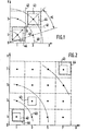
- the lines 41, 42 and the axes OX and OY define the decision zones for the states of the quarter plane shown in FIG. 1.
- the received point will move on a circle centered in 0 and passing through the particular state.
- On the circle 40 appears a position A which corresponds to the smallest distance between the circle 40 and the state (3,3).
- a detected state located at A is interpreted as being a state (3.3) whereas it is a state (3.1) or a state (1.3) with a phase difference.
- the invention defines around each state an acquisition zone 43 which does not come into contact with the circle 40 for the example chosen.
- the states selected for acquisition are states (1,1) and (3,3) because in fact the phase difference between the 4 type states ( ⁇ 1, ⁇ 1), as well as between the 4 type states ( ⁇ 3, ⁇ 3), is ⁇ / 2.
- phase error modulo ⁇ / 2
- the invention therefore selects the states which have the same symmetry as the modulation itself and defines around each state an area where the acquisition can be carried out.
- the acquisition area 43 is centered on the selected state.
- the acquisition area 44 is eccentric.
- Figure 2 shows the same type of representation for a 64 MAQ modulation.
- the acquisition problems are much more numerous due to the existence of a large number of states which can lead to a disturbance of the mechanism d 'acquisition.
- the selected states are the states (1,1), (3,3), (7,7) which have an order of symmetry identical to that of the modulation itself.
- the state (5, 5) cannot be selected because it is on the circle which passes through the states (1, 7) and (7, 1).
- an acquisition zone 43 or 44 is defined in which the acquisition must take place, this acquisition zone not coming into contact with the circles passing through the other states.
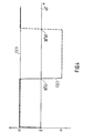
- FIG. 3 shows in B the characteristics of a phase comparator for a phase between -w / M and + ⁇ / M.
- the phase comparator delivers a voltage which is a function of the phase difference which makes it possible to control the frequency of the oscillator.
- the comparator output voltage is shown in C.
- the average value of this output voltage is zero.
- the value of the output voltage of the phase comparator is memorized using selection and acquisition means which characterize the invention.
- an acquisition circuit stores the state of the comparator output signal.
- Such a stored signal is represented in D, its average value is no longer zero. It allows the frequency correction of the oscillator to be carried out.
- the curves C and D of FIG. 3 are representative of a positive frequency deviation, that is to say a frequency of the modulated wave carrier greater than the frequency of the oscillator. For a negative frequency difference the curves C and D have an inverted shape.
- FIG. 4 represents, in the case of an MAQ 16 modulation, the state of the output signal of a phase comparator for a phase difference varying from 0 to v / 4. This domain is sufficient because the characteristic of the comparator is periodic of v / 2 and is odd.
- Such a comparator will deliver a signal which, examined over a half-period (O, w / 4), will present certain singularities depending on the state of the constellation studied.
- the half-period (0, ⁇ / 4), that is to say half of the symmetry, we note that certain states will lead to transitions by zero of the output of the comparator but for which the error of phase is not zero.
- Figure 4 shows that a state (3,1) can lead to zero transitions of the comparator output which must be eliminated to carry out the acquisition.
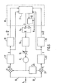
- FIG. 5 represents the block diagram of the carrier wave recovery circuit.
- the digitally modulated wave arrives at the input connection 5 and is subdivided into two channels 10 and 20 respectively in phase and in quadrature with the wave of the oscillator 17.
- the latter delivers its signal directly to the demodulator 11 of the channel in phase, and also to the demodulator 21 of the quadrature channel through the phase shifter of r / 2 24.
- the outputs of the demodulators 11 and 21 are filtered respectively in the low-pass filters 12 and 22 having the output signal respectively X and Y.
- the error signals e x and ey as well as the filtered signals X and Y enter the phase comparison device 30, which also receives the base clock H and which delivers the binary comparison signal S and the clock d 'sampling.
- These two signals enter a flip-flop 14 whose data input receives the comparison signal S and the clock input receives the sampling clock from the selection and comparison means 31 and the generation means 32 constituting the phase comparison device 30 which contains the invention.
- the output signal of the flip-flop 14 passes through a low-pass filter 15 then through an amplifier 16 to supply the control signal ⁇ ( ⁇ ) which controls the oscillator 17.
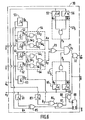
- the signals A x and Ay enter a NON-OR-exclusive gate 70 whose output enters, with the signals P x and Py, in an AND gate 71 which delivers the signal P z .
- This signal P z indicates whether the point (X, Y) received belongs or does not belong to the particular zones which it is desired to detect.
- the signal P z and the base clock H enter an AND gate 32 which delivers the sampling clock He.
- the outputs of comparators 81 and 53 enter an exclusive OR gate 85 and the outputs of comparators 83 and 63 enter an exclusive OR gate 86.
- the outputs of doors 85 and 86 enter an exclusive OR gate 87 whose output enters, with the base clock H, in an AND gate 88 which delivers a signal which serves as a clock for a flip-flop 89 whose input data come from the output of the OR-exclusive gate 85.
- This flip-flop 89 delivers an output signal S which enters the data input of the flip-flop 14 of FIG. 5, the clock of the latter being constituted by the sampling clock.
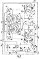
- FIG. 7 represents the logic diagram of an exemplary embodiment of the phase comparison device 30, according to the invention, in the case of zones eccentric on the diagonal states of a constellation MAQ 16.
- a first difference lies in the fact that the signals Ny, My and Qy enter a selection circuit 67 which performs the logical operation defined by:
- a second difference lies in the fact that the signals N x , M x and Q x enter a selection circuit 57 which performs the logic operation defined by:
Landscapes
- Engineering & Computer Science (AREA)
- Computer Networks & Wireless Communication (AREA)
- Signal Processing (AREA)
- Digital Transmission Methods That Use Modulated Carrier Waves (AREA)
- Communication Control (AREA)
Applications Claiming Priority (2)
| Application Number | Priority Date | Filing Date | Title |
|---|---|---|---|
| FR8506561 | 1985-04-30 | ||
| FR8506561A FR2581277A1 (fr) | 1985-04-30 | 1985-04-30 | Circuit de recuperation de l'onde porteuse de systemes de transmissions numeriques |
Publications (2)
| Publication Number | Publication Date |
|---|---|
| EP0200271A1 true EP0200271A1 (de) | 1986-11-05 |
| EP0200271B1 EP0200271B1 (de) | 1990-01-31 |
Family
ID=9318824
Family Applications (1)
| Application Number | Title | Priority Date | Filing Date |
|---|---|---|---|
| EP86200712A Expired - Lifetime EP0200271B1 (de) | 1985-04-30 | 1986-04-25 | Trägerrückgewinnungsschaltung für digitale Übertragungssysteme |
Country Status (9)
| Country | Link |
|---|---|
| US (1) | US4687999A (de) |
| EP (1) | EP0200271B1 (de) |
| JP (1) | JPH0793644B2 (de) |
| AU (1) | AU5676986A (de) |
| CA (1) | CA1256953A (de) |
| DE (1) | DE3668741D1 (de) |
| FI (1) | FI86126C (de) |
| FR (1) | FR2581277A1 (de) |
| NO (1) | NO172670C (de) |
Cited By (5)
| Publication number | Priority date | Publication date | Assignee | Title |
|---|---|---|---|---|
| FR2620885A1 (fr) * | 1987-09-18 | 1989-03-24 | Alcatel Thomson Faisceaux | Procede de detection de faux accrochages du signal reference sur le signal a demoduler en demodulation numerique coherente et dispositif mettant en oeuvre un tel procede |
| GB2282030A (en) * | 1993-09-14 | 1995-03-22 | Plessey Semiconductors Ltd | Direct conversion receivers |
| EP0703687A1 (de) * | 1994-09-23 | 1996-03-27 | France Telecom | Trägerrückwinnung für PSK Signale |
| EP0719002A1 (de) * | 1994-12-22 | 1996-06-26 | ALCATEL BELL Naamloze Vennootschap | Prozessor für Trägerrückgewinnung |
| EP1940104A3 (de) * | 2006-12-29 | 2012-07-25 | Trident Microsystems (Far East) Ltd. | Vorrichtung und Verfahren zum Entscheiden eines Symbols beim Empfang eines mit einem Quadratursignalpaar gekoppelten Signals zur QAM-Frequenzregelung und/oder Rotationsregelung |
Families Citing this family (36)
| Publication number | Priority date | Publication date | Assignee | Title |
|---|---|---|---|---|
| DE3619744A1 (de) * | 1986-06-12 | 1987-12-17 | Ant Nachrichtentech | Verfahren zum gewinnen eines phasendifferenzsignals |
| US4860320A (en) * | 1986-06-12 | 1989-08-22 | Ant Nachrichtentechnik Gmbh | Method for recovering a control signal for controlling the phase of a local carrier signal |
| DE3766614D1 (de) * | 1987-03-10 | 1991-01-17 | Ant Nachrichtentech | Verfahren zum gewinnen eines phasendifferenzsignals. |
| US4736386A (en) * | 1987-04-06 | 1988-04-05 | Rockwell International Corporation | Carrier out-of-lock detector apparatus |
| US4771438A (en) * | 1987-08-04 | 1988-09-13 | Hayes Microcomputer Products, Inc. | Method and apparatus for phase reference recovery in high speed fast turnaround modem |
| FR2621188B1 (fr) * | 1987-09-25 | 1989-12-29 | Labo Electronique Physique | Circuit de recuperation de l'onde porteuse de systemes de transmissions numeriques |
| FR2627653B1 (fr) * | 1988-02-18 | 1994-04-08 | Alcatel Thomson Faisceaux Hertzi | Procede d'asservissement de l'instant de regeneration dans une transmission numerique utilisant une modulation de porteuse selon deux axes en quadrature et dispositif de mise en oeuvre de ce procede |
| JPH02217045A (ja) * | 1989-02-17 | 1990-08-29 | Fujitsu Ltd | 信号点配置方式 |
| US4959844A (en) * | 1989-10-24 | 1990-09-25 | Amp Incorporated | Clock recovery circuit for digital demodulator |
| US5287351A (en) * | 1990-11-27 | 1994-02-15 | Scientific-Atlanta, Inc. | Method and apparatus for minimizing error propagation in correlative digital and communication system |
| AU1918892A (en) * | 1991-05-10 | 1992-12-30 | Echelon Corporation | Power line communication while avoiding determinable interference harmonics |
| US5271041A (en) * | 1992-03-16 | 1993-12-14 | Scientific-Atlanta, Inc. | Method and apparatus for QPR carrier recovery |
| US5528632A (en) * | 1994-07-28 | 1996-06-18 | Motorola, Inc. | Non-complex dual-correlation phase reversal detector and method |
| JP3540393B2 (ja) * | 1994-10-31 | 2004-07-07 | 三洋電機株式会社 | コスタスループ |
| AUPN455695A0 (en) * | 1995-08-01 | 1995-08-24 | Canon Kabushiki Kaisha | Qam spread spectrum demodulation system |
| US5640425A (en) * | 1995-12-26 | 1997-06-17 | Golden Bridge Technology, Inc. | Fast-acting costas loop |
| EP0895386B1 (de) * | 1997-07-31 | 2003-01-29 | Micronas Semiconductor Holding AG | Trägerregelkreis für einen Empfänger von digital übertragenen Signalen |
| DE19733732C2 (de) * | 1997-08-04 | 1999-05-12 | Siemens Ag | Verfahren zur Unterstützung der einfachen Synchronisierung auf den Träger eines energieverwischten QPSK-Signals |
| US6738429B1 (en) * | 1999-06-01 | 2004-05-18 | Harris Corporation | Decision-directed carrier frequency detector and method for QAM |
| EP1503500B1 (de) * | 2003-07-28 | 2006-06-28 | Frank Dr.-Ir. Op 't Eynde | Phasenregelkreis |
| US7355470B2 (en) | 2006-04-24 | 2008-04-08 | Parkervision, Inc. | Systems and methods of RF power transmission, modulation, and amplification, including embodiments for amplifier class transitioning |
| US7327803B2 (en) * | 2004-10-22 | 2008-02-05 | Parkervision, Inc. | Systems and methods for vector power amplification |
| US8041538B2 (en) * | 2005-07-05 | 2011-10-18 | Stmicroelectronics S.A. | Estimating of the amplitude of a noisy binary signal |
| RU2296432C1 (ru) * | 2005-10-07 | 2007-03-27 | Военно-космическая академия имени А.Ф. Можайского | Способ автокорреляционного приема шумоподобных сигналов |
| US7911272B2 (en) * | 2007-06-19 | 2011-03-22 | Parkervision, Inc. | Systems and methods of RF power transmission, modulation, and amplification, including blended control embodiments |
| US8334722B2 (en) | 2007-06-28 | 2012-12-18 | Parkervision, Inc. | Systems and methods of RF power transmission, modulation and amplification |
| US9106316B2 (en) | 2005-10-24 | 2015-08-11 | Parkervision, Inc. | Systems and methods of RF power transmission, modulation, and amplification |
| RU2309550C1 (ru) * | 2006-02-22 | 2007-10-27 | Институт Прикладной Астрономии Российской Академии Наук | Способ автокорреляционного приема шумоподобного сигнала |
| US8031804B2 (en) | 2006-04-24 | 2011-10-04 | Parkervision, Inc. | Systems and methods of RF tower transmission, modulation, and amplification, including embodiments for compensating for waveform distortion |
| WO2008144017A1 (en) | 2007-05-18 | 2008-11-27 | Parkervision, Inc. | Systems and methods of rf power transmission, modulation, and amplification |
| WO2008156800A1 (en) | 2007-06-19 | 2008-12-24 | Parkervision, Inc. | Combiner-less multiple input single output (miso) amplification with blended control |
| RU2422989C1 (ru) * | 2010-01-11 | 2011-06-27 | Открытое акционерное общество "Концерн "Созвездие" | Способ передачи информации широкополосными псевдослучайными сигналами |
| KR20140026458A (ko) | 2011-04-08 | 2014-03-05 | 파커비전, 인크. | Rf 전력 송신, 변조 및 증폭 시스템들 및 방법들 |
| KR20140034895A (ko) | 2011-06-02 | 2014-03-20 | 파커비전, 인크. | 안테나 제어 |
| CN106415435B (zh) | 2013-09-17 | 2020-08-11 | 帕克维辛股份有限公司 | 用于呈现信息承载时间函数的方法、装置和系统 |
| CN113872902B (zh) * | 2020-06-30 | 2023-04-07 | 华为技术有限公司 | 信号调制电路、方法及相关产品 |
Citations (5)
| Publication number | Priority date | Publication date | Assignee | Title |
|---|---|---|---|---|
| US3970946A (en) * | 1973-07-12 | 1976-07-20 | Nippon Electric Company, Ltd. | Demodulator for amplitude-and-phase modulated signals having control means for reducing phase and amplitude errors |
| US4057762A (en) * | 1975-12-26 | 1977-11-08 | Nippon Electric Company, Ltd. | Device for phase synchronizing a reproduced reference carrier signal with windows specified for preselected ones of amplitude and phase modulated signal points |
| US4334312A (en) * | 1979-08-10 | 1982-06-08 | Nippon Electric Co., Ltd. | Phase synchronizing circuit for use in multi-level, multi-phase, superposition-modulated signal transmission system |
| EP0118156A1 (de) * | 1983-03-07 | 1984-09-12 | Telecommunications Radioelectriques Et Telephoniques T.R.T. | Schaltung zur Trägerrückgewinnung für ein in Amplituden- und Phasenstufen moduliertes Signal |
| FR2552959A1 (fr) * | 1983-10-04 | 1985-04-05 | Vandamme Patrick | Circuit de recuperation d'une onde porteuse muni d'un moyen d'aide a l'acquisition automatique et rapide |
Family Cites Families (2)
| Publication number | Priority date | Publication date | Assignee | Title |
|---|---|---|---|---|
| JPS5820181B2 (ja) * | 1974-09-25 | 1983-04-21 | 日本電気株式会社 | タソウイソウドウキフクチヨウソウチ |
| US4571550A (en) * | 1984-06-22 | 1986-02-18 | Rockwell International Corporation | QAM Demodulator carrier recovery loop using n-m LSB's |
-
1985
- 1985-04-30 FR FR8506561A patent/FR2581277A1/fr not_active Withdrawn
-
1986
- 1986-04-23 US US06/855,527 patent/US4687999A/en not_active Expired - Lifetime
- 1986-04-24 CA CA000507482A patent/CA1256953A/en not_active Expired
- 1986-04-25 EP EP86200712A patent/EP0200271B1/de not_active Expired - Lifetime
- 1986-04-25 FI FI861757A patent/FI86126C/fi not_active IP Right Cessation
- 1986-04-25 DE DE8686200712T patent/DE3668741D1/de not_active Expired - Lifetime
- 1986-04-28 NO NO861664A patent/NO172670C/no unknown
- 1986-04-28 AU AU56769/86A patent/AU5676986A/en not_active Abandoned
- 1986-04-30 JP JP61098394A patent/JPH0793644B2/ja not_active Expired - Lifetime
Patent Citations (5)
| Publication number | Priority date | Publication date | Assignee | Title |
|---|---|---|---|---|
| US3970946A (en) * | 1973-07-12 | 1976-07-20 | Nippon Electric Company, Ltd. | Demodulator for amplitude-and-phase modulated signals having control means for reducing phase and amplitude errors |
| US4057762A (en) * | 1975-12-26 | 1977-11-08 | Nippon Electric Company, Ltd. | Device for phase synchronizing a reproduced reference carrier signal with windows specified for preselected ones of amplitude and phase modulated signal points |
| US4334312A (en) * | 1979-08-10 | 1982-06-08 | Nippon Electric Co., Ltd. | Phase synchronizing circuit for use in multi-level, multi-phase, superposition-modulated signal transmission system |
| EP0118156A1 (de) * | 1983-03-07 | 1984-09-12 | Telecommunications Radioelectriques Et Telephoniques T.R.T. | Schaltung zur Trägerrückgewinnung für ein in Amplituden- und Phasenstufen moduliertes Signal |
| FR2552959A1 (fr) * | 1983-10-04 | 1985-04-05 | Vandamme Patrick | Circuit de recuperation d'une onde porteuse muni d'un moyen d'aide a l'acquisition automatique et rapide |
Non-Patent Citations (2)
| Title |
|---|
| ELECTRONICS & COMMUNICATIONS IN JAPAN, vol. 63, no. 7, 1980, pages 75-84, Scripta Publishing Co., Silver Spring, Maryland, US; I. HORIKAWA et al.: "16-QAM carrier recovery with selective gated phase-locked loop" * |
| IEEE TRANSACTIONS ON COMMUNICATIONS, vol. COM-31, no. 1, janvier 1983, pages 130-136, IEEE, New York, US; A. LECLERT et al.: "Universal carrier recovery loop for QASK and PSK signal sets" * |
Cited By (12)
| Publication number | Priority date | Publication date | Assignee | Title |
|---|---|---|---|---|
| FR2620885A1 (fr) * | 1987-09-18 | 1989-03-24 | Alcatel Thomson Faisceaux | Procede de detection de faux accrochages du signal reference sur le signal a demoduler en demodulation numerique coherente et dispositif mettant en oeuvre un tel procede |
| EP0309306A1 (de) * | 1987-09-18 | 1989-03-29 | Alcatel Telspace | Verfahren zur Detektion eines Phasenfehlers zwischen Referenzsignal und zu demodulierendem Signal bei kohärenter digitaler Demodulation und Vorrichtung zur Durchführung des Verfahrens |
| US4847578A (en) * | 1987-09-18 | 1989-07-11 | Alcatel Thomson Faiscequx Hertziens | Method and device for detecting false locks between a reference signal and a signal to be demodulated by coherent digital demodulation |
| GB2282030A (en) * | 1993-09-14 | 1995-03-22 | Plessey Semiconductors Ltd | Direct conversion receivers |
| US5451899A (en) * | 1993-09-14 | 1995-09-19 | Plessey Semiconductors Limited | Direct conversion FSK receiver using frequency tracking filters |
| GB2282030B (en) * | 1993-09-14 | 1997-09-24 | Plessey Semiconductors Ltd | Direct conversion receiver |
| EP0703687A1 (de) * | 1994-09-23 | 1996-03-27 | France Telecom | Trägerrückwinnung für PSK Signale |
| FR2725097A1 (fr) * | 1994-09-23 | 1996-03-29 | France Telecom | Procede et dispositif d'evaluation numerique de la phase d'une porteuse modulee |
| US5740202A (en) * | 1994-09-23 | 1998-04-14 | France Telecom | Method and apparatus for digitally evaluating the phase of a modulated carrier |
| EP0719002A1 (de) * | 1994-12-22 | 1996-06-26 | ALCATEL BELL Naamloze Vennootschap | Prozessor für Trägerrückgewinnung |
| US5657355A (en) * | 1994-12-22 | 1997-08-12 | Alcatel N.V. | Signal processor module |
| EP1940104A3 (de) * | 2006-12-29 | 2012-07-25 | Trident Microsystems (Far East) Ltd. | Vorrichtung und Verfahren zum Entscheiden eines Symbols beim Empfang eines mit einem Quadratursignalpaar gekoppelten Signals zur QAM-Frequenzregelung und/oder Rotationsregelung |
Also Published As
| Publication number | Publication date |
|---|---|
| FI86126B (fi) | 1992-03-31 |
| EP0200271B1 (de) | 1990-01-31 |
| CA1256953A (en) | 1989-07-04 |
| FI86126C (fi) | 1992-07-10 |
| AU5676986A (en) | 1986-11-06 |
| FI861757A7 (fi) | 1986-10-31 |
| NO861664L (no) | 1986-10-31 |
| DE3668741D1 (de) | 1990-03-08 |
| FR2581277A1 (fr) | 1986-10-31 |
| JPH0793644B2 (ja) | 1995-10-09 |
| US4687999A (en) | 1987-08-18 |
| JPS61253959A (ja) | 1986-11-11 |
| FI861757A0 (fi) | 1986-04-25 |
| NO172670C (no) | 1993-08-18 |
| NO172670B (no) | 1993-05-10 |
Similar Documents
| Publication | Publication Date | Title |
|---|---|---|
| EP0200271B1 (de) | Trägerrückgewinnungsschaltung für digitale Übertragungssysteme | |
| EP0309038B1 (de) | Schaltung zur Regenerierung des Trägers für Datenübertragungsanordnungen | |
| EP0071514B1 (de) | Einrichtung zur Rückgewinnung von Trägerwellen | |
| EP0530107B1 (de) | PSK-Demodulator mit Korrektur im Basisband für Phasen- oder Frequenzfehler | |
| FR2494059A1 (fr) | Procede et dispositif de demodulation de porteuse a acquisition rapide | |
| FR2523388A1 (fr) | Dispositif a seuil adaptatif | |
| FR2880482A1 (fr) | Dispositif de conversion d'un signal transmis en un signal numerique | |
| FR2713855A1 (fr) | Procédé de détection de décrochage de récupération de porteuse et de détermination du rapport EB/NO d'une liaison de transmission numérique et dispositif mettant en Óoeuvre ce procédé. | |
| EP0459968B1 (de) | Digitaler Demodulator für mehrphasenmodulierte Signale | |
| CA2201387A1 (fr) | Estimateur et recuperateur de phase robuste pour signaux numeriques affectes notamment de gigue de phase | |
| EP0352159B1 (de) | Frequenzabweichungstolerierendes Verfahren und Vorrichtung zur Demodulation von, durch eine Binärsymbolreihe, winkelmodulierten Signalen mit konstanter Umhüllung und kontinuierlicher Phase | |
| EP0063842B1 (de) | Trägerrückgewinnung für eine Amplituden- und Phasenmodulation mit 16 Zuständen und Empfangssystem für digitale Daten, welches eine solche Einrichtung enthält | |
| FR2466145A1 (fr) | Circuit de synchronisation de phases pour systeme de transmission de signaux modules par superposition a phases multiples, a niveaux multiples | |
| EP0230900B1 (de) | Taktwiedergewinnungseinrichtung | |
| EP0285954B1 (de) | Automatischer Entzerrer für digitale Übertragung | |
| CA1312657C (fr) | Dispositif de synchronisation en modulation de phase a quatre etats decalee | |
| FR2824977A1 (fr) | Procede de demodulation et de modulation d'un signal tenant compte de l'effet d'erreurs de phase, recepteur, systeme et signal correspondants | |
| EP2504963B1 (de) | System und verfahren zum senden und zum empfangen eines digitalen funksignals | |
| FR2552959A1 (fr) | Circuit de recuperation d'une onde porteuse muni d'un moyen d'aide a l'acquisition automatique et rapide | |
| FR2758038A1 (fr) | Dispositif d'estimation de l'ecart de frequence existant entre la frequence porteuse d'un signal numerique et la frequence d'un oscillateur local de reception, et recepteur correspondant | |
| FR2663177A1 (fr) | Dispositif de recuperation d'une onde porteuse muni d'un moyen d'inhibition de faux accrochages en frequence. | |
| FR2812985A1 (fr) | Circuit de demodulation d'un signal logique transmis par des voies analogiques | |
| EP0309306B1 (de) | Verfahren zur Detektion eines Phasenfehlers zwischen Referenzsignal und zu demodulierendem Signal bei kohärenter digitaler Demodulation und Vorrichtung zur Durchführung des Verfahrens | |
| WO2005083964A1 (fr) | Procede de reception multi modulation s’appliquant à la demodulation de signaux issus de modulations dont les symboles sont inclus dans une constellation principale | |
| EP0683946B1 (de) | System zum empfang oder lesen eines informationsstromes durch abtastung in regelmässigen abständen |
Legal Events
| Date | Code | Title | Description |
|---|---|---|---|
| PUAI | Public reference made under article 153(3) epc to a published international application that has entered the european phase |
Free format text: ORIGINAL CODE: 0009012 |
|
| AK | Designated contracting states |
Kind code of ref document: A1 Designated state(s): BE CH DE FR GB IT LI NL SE |
|
| 17P | Request for examination filed |
Effective date: 19870505 |
|
| 17Q | First examination report despatched |
Effective date: 19890517 |
|
| GRAA | (expected) grant |
Free format text: ORIGINAL CODE: 0009210 |
|
| RAP1 | Party data changed (applicant data changed or rights of an application transferred) |
Owner name: N.V. PHILIPS' GLOEILAMPENFABRIEKEN Owner name: LABORATOIRES D'ELECTRONIQUE PHILIPS |
|
| AK | Designated contracting states |
Kind code of ref document: B1 Designated state(s): BE CH DE FR GB IT LI NL SE |
|
| REF | Corresponds to: |
Ref document number: 3668741 Country of ref document: DE Date of ref document: 19900308 |
|
| ITF | It: translation for a ep patent filed | ||
| PGFP | Annual fee paid to national office [announced via postgrant information from national office to epo] |
Ref country code: NL Payment date: 19900430 Year of fee payment: 5 |
|
| GBT | Gb: translation of ep patent filed (gb section 77(6)(a)/1977) | ||
| PLBE | No opposition filed within time limit |
Free format text: ORIGINAL CODE: 0009261 |
|
| STAA | Information on the status of an ep patent application or granted ep patent |
Free format text: STATUS: NO OPPOSITION FILED WITHIN TIME LIMIT |
|
| 26N | No opposition filed | ||
| PG25 | Lapsed in a contracting state [announced via postgrant information from national office to epo] |
Ref country code: NL Effective date: 19911101 |
|
| NLV4 | Nl: lapsed or anulled due to non-payment of the annual fee | ||
| PGFP | Annual fee paid to national office [announced via postgrant information from national office to epo] |
Ref country code: BE Payment date: 19930429 Year of fee payment: 8 |
|
| PGFP | Annual fee paid to national office [announced via postgrant information from national office to epo] |
Ref country code: CH Payment date: 19930720 Year of fee payment: 8 |
|
| ITTA | It: last paid annual fee | ||
| PG25 | Lapsed in a contracting state [announced via postgrant information from national office to epo] |
Ref country code: LI Effective date: 19940430 Ref country code: CH Effective date: 19940430 Ref country code: BE Effective date: 19940430 |
|
| BERE | Be: lapsed |
Owner name: PHILIPS' GLOEILAMPENFABRIEKEN N.V. Effective date: 19940430 Owner name: LABORATOIRES D'ELECTRONIQUE PHILIPS Effective date: 19940430 |
|
| REG | Reference to a national code |
Ref country code: CH Ref legal event code: PL |
|
| EAL | Se: european patent in force in sweden |
Ref document number: 86200712.7 |
|
| ITPR | It: changes in ownership of a european patent |
Owner name: CAMBIO RAGIONE SOCIALE;PHILIPS ELECTRONICS N.V. |
|
| REG | Reference to a national code |
Ref country code: FR Ref legal event code: CJ Ref country code: FR Ref legal event code: CD |
|
| PGFP | Annual fee paid to national office [announced via postgrant information from national office to epo] |
Ref country code: SE Payment date: 19960425 Year of fee payment: 11 |
|
| PG25 | Lapsed in a contracting state [announced via postgrant information from national office to epo] |
Ref country code: SE Effective date: 19970426 |
|
| EUG | Se: european patent has lapsed |
Ref document number: 86200712.7 |
|
| PGFP | Annual fee paid to national office [announced via postgrant information from national office to epo] |
Ref country code: GB Payment date: 19990420 Year of fee payment: 14 |
|
| PGFP | Annual fee paid to national office [announced via postgrant information from national office to epo] |
Ref country code: FR Payment date: 19990427 Year of fee payment: 14 |
|
| PGFP | Annual fee paid to national office [announced via postgrant information from national office to epo] |
Ref country code: DE Payment date: 19990624 Year of fee payment: 14 |
|
| REG | Reference to a national code |
Ref country code: FR Ref legal event code: TP |
|
| PG25 | Lapsed in a contracting state [announced via postgrant information from national office to epo] |
Ref country code: GB Free format text: LAPSE BECAUSE OF NON-PAYMENT OF DUE FEES Effective date: 20000425 |
|
| GBPC | Gb: european patent ceased through non-payment of renewal fee |
Effective date: 20000425 |
|
| PG25 | Lapsed in a contracting state [announced via postgrant information from national office to epo] |
Ref country code: FR Free format text: LAPSE BECAUSE OF NON-PAYMENT OF DUE FEES Effective date: 20001229 |
|
| PG25 | Lapsed in a contracting state [announced via postgrant information from national office to epo] |
Ref country code: DE Free format text: LAPSE BECAUSE OF NON-PAYMENT OF DUE FEES Effective date: 20010201 |
|
| REG | Reference to a national code |
Ref country code: FR Ref legal event code: ST |
|
| PG25 | Lapsed in a contracting state [announced via postgrant information from national office to epo] |
Ref country code: IT Free format text: LAPSE BECAUSE OF NON-PAYMENT OF DUE FEES;WARNING: LAPSES OF ITALIAN PATENTS WITH EFFECTIVE DATE BEFORE 2007 MAY HAVE OCCURRED AT ANY TIME BEFORE 2007. THE CORRECT EFFECTIVE DATE MAY BE DIFFERENT FROM THE ONE RECORDED. Effective date: 20050425 |