EP0200241B1 - Detektor für thermische Strahlung - Google Patents
Detektor für thermische Strahlung Download PDFInfo
- Publication number
- EP0200241B1 EP0200241B1 EP86200478A EP86200478A EP0200241B1 EP 0200241 B1 EP0200241 B1 EP 0200241B1 EP 86200478 A EP86200478 A EP 86200478A EP 86200478 A EP86200478 A EP 86200478A EP 0200241 B1 EP0200241 B1 EP 0200241B1
- Authority
- EP
- European Patent Office
- Prior art keywords
- detecting means
- flexible film
- layer
- detector
- radiation
- Prior art date
- Legal status (The legal status is an assumption and is not a legal conclusion. Google has not performed a legal analysis and makes no representation as to the accuracy of the status listed.)
- Expired - Lifetime
Links
Images

Classifications
-
- H—ELECTRICITY
- H10—SEMICONDUCTOR DEVICES; ELECTRIC SOLID-STATE DEVICES NOT OTHERWISE PROVIDED FOR
- H10N—ELECTRIC SOLID-STATE DEVICES NOT OTHERWISE PROVIDED FOR
- H10N15/00—Thermoelectric devices without a junction of dissimilar materials; Thermomagnetic devices, e.g. using the Nernst-Ettingshausen effect
- H10N15/10—Thermoelectric devices using thermal change of the dielectric constant, e.g. working above and below the Curie point
-
- G—PHYSICS
- G01—MEASURING; TESTING
- G01J—MEASUREMENT OF INTENSITY, VELOCITY, SPECTRAL CONTENT, POLARISATION, PHASE OR PULSE CHARACTERISTICS OF INFRARED, VISIBLE OR ULTRAVIOLET LIGHT; COLORIMETRY; RADIATION PYROMETRY
- G01J5/00—Radiation pyrometry, e.g. infrared or optical thermometry
- G01J5/10—Radiation pyrometry, e.g. infrared or optical thermometry using electric radiation detectors
- G01J5/34—Radiation pyrometry, e.g. infrared or optical thermometry using electric radiation detectors using capacitors, e.g. pyroelectric capacitors
Definitions
- the invention relates to a thermal radiation detector comprising means having a temperature-dependent characteristic for detecting thermal energy, wherein the detecting means are supported by at least one flexible film which is substantially transparent in the wavelength range of the radiation to be detected in operation, and wherein with respect to the direction of incidence of thermal radiation to be detected, said one flexible film precedes the detecting means.
- the invention further relates to an array of such detectors.
- a detector as set forth in the opening sentence wherein the detecting means comprise an element of pyroelectric material is known from European Patent Application EP-A-0041297.
- the element of pyroelectric material is supported by and between two flexible plastics films of polyimide material around 0.85»m in thickness which transmit approximately 80% of incident radiation in the wavelength range of 8-14»m, and the detector is adapted for infrared radiation that is to be detected to be incident on one of the plastics films.
- the plastics films support electrically conductive layers providing electrical connections to the pyroelectric element. This arrangement enables the detector to have particularly low susceptibility to microphony as well as low lateral thermal conductance.
- thermal radiation detectors A problem with thermal radiation detectors is to absorb sufficient of the incident radiation.
- pyroelectric materials suitable for good-quality detectors typically have rather low absorption over at least part of the wavelength range for which it is desirable to provide such detectors; furthermore, the thinner the detector (a feature which is desirable to reduce particularly thermal capacitance as well as its thermal conductance to the surroundings), the lower will be the overall absorption of the incident radiation by the pyroelectric material.
- a conventional way of improving absorption has been to apply a "black" (blackening); however, appropriate materials have the disadvantages of being awkward to apply and having poor adhesion.
- LaDelfe et al refers to the work of Annis and Simpson ("Absorption of Radiation in PLZT Pyroelectric Detectors", Infrared Physics, Volume 14 (1974), pages 199-205) who applied the theoretical work of Hadley & Dennison, Hilsum and Silberg to a three-layer structure wherein the dielectric sandwiched between the two metal layers was the pyroelectric material itself and had a thickness of 10-15»m, giving an optical thickness of roughly 21 ⁇ 2 wavelengths in a typical operating range.
- LaDelfe et al themselves applied a two-layer coating consisting of a metal layer and an anti-reflection layer to chips of pyroelectric material 0.25 mm thick.
- a thermal radiation detector for detecting radiation in a selected wavelength range, comprising means having a temperature-dependent characteristic for detecting thermal energy, wherein the detecting means are supported by at least one flexible film which is substantially transparent in said wavelength range, and wherein with respect to the direction of incidence of thermal radiation to be detected, said one flexible film precedes the detecting means, characterised in that the detector comprises an electrically resistive layer which has a net effective resistance per square of substantially 377/(1+n2) ohms per square, where n is the refractive index of said one flexible film, and is disposed immediately adjacent said one flexible film between the flexible film and the detecting means whereby to absorb incident radiation in said wavelength range, in that the detecting means are thermally coupled to the resistive layer, and in that the optical thickness of substantially transparent dielectric material preceding the detecting means and comprising said one flexible film is one quarter of a selected wavelength in said wavelength range.
- a thermal radiation detector for detecting radiation in a selected wavelength range, comprising means having a temperature-dependent characteristic for detecting thermal energy, wherein the detecting means are supported by at least one flexible film which is substantially transparent in said wavelength range, and wherein with respect to the direction of incidence of thermal radiation to be detected, said one flexible film precedes the detecting means, characterised in that the detector comprises an electrically resistive layer which is disposed immediately adjacent the side of said one flexible film remote from the detecting means and which has a net effective resistance per square so as to absorb incident radiation in said wavelength range, in that a reflecting, electrically conductive, layer, which reflects incident radiation in the thermal radiation range, substantially coextensive with the resistive layer is disposed between said one flexible film and the detecting means, in that the detecting means are thermally coupled to the resistive layer, and in that the optical thickness of substantially transparent dielectric material preceding the detecting means and comprising said one flexible film is one quarter of a selected wavelength in said wavelength range.
- the optical thickness of said one flexible film is one quarter of said selected wavelength. This avoids difficulties such as "crazing" which would be liable to arise if a layer of suitable dielectric material, which typically is brittle, were to be deposited on a flexible film to make up a total optical thickness of a quarter of the selected wavelength.
- the invention involves the recognition that a flexible film which is used to support the detecting means and which can provide the mechanical advantage of low microphony and the thermal advantage of low thermal conductance can also be used as part or, preferably, the whole of the thickness of a quarter-wavelength optical layer in combination with an electrically resistive layer for improving the absorption of incident thermal radiation.
- the resistive layer has a net effective resistance per square such that it absorbs a substantial proportion of incident radiation in the wavelength range.
- the selected wavelength is that at which it is desired that the absorption of incident radiation by the resistive layer should be substantially a maximum.
- the electrically resistive layer is electrically in parallel with one or more adjacent further layers having some electrical conductivity, then either the resistance per square of the further layer(s) should be sufficiently high not substantially to reduce the effective resistance per square of the first-mentioned electrically resistive layer, or the resistance per square of said electrically resistive layer should be selected so that in combination with the further layer(s), its net effective resistance per square has a suitable value for substantially absorbing radiation in the desired operating wavelength range.
- a detector embodying the invention can be relatively easy to make, and the means used to improve the absorption of radiation need add only relatively little thermal capacitance to the detector.
- Said selected wavelength may be such as substantially to maximise the absorption of incident radiation by the detector over said wavelength range.
- UK Patent Application GB 2 100 058 A discloses a thermal radiation detector comprising an element of pyroelectric material supported by and between two flexible films of polyimide material each having a thickness of about 1»m and further comprising a layer for absorbing incident radiation that is disposed between one of the flexible films and the pyroelectric element; the absorbing layer may be of antimony 50 nm thick.
- the absorbing layer is contiguous with a coextensive electrically conductive further layer which may be of aluminium about 0.5»m thick.
- the latter layer has a very low resistance per square, so that the net effective resistance per square of the absorbing layer is at least as low. Consequently, the absorption of incident radiation by the absorbing layer will depend on processes not concerned with the electrical conductance of the layer.
- the resistive layer may be immediately preceded by free space, and in this case the resistive layer suitably has a resistance per square substantially equal to the characteristic impedance of free space.
- the total thermal capacitance of said layer or layers and of the portion of said one flexible film coextensive therewith is much less than the thermal capacitance of the detecting means.
- a layer may supply to the detecting means at said surface thereof thermal energy from radiation incident on every part of said resistive layer.
- This aspect of the present invention involves the recognition that the layer disposed between the detecting means and the flexible film in an embodiment of the present invention can extend substantially beyond at least part of the periphery of the adjacent face of the detecting means and can be used to supply to the detecting means at that face thermal energy from radiation incident on an operative surface region larger than that face.
- the layer disposed between the detecting means and the flexible film is a resistive layer
- the extent of that layer generally constitutes the operative surface region of the detector, and thermal energy from radiation incident on a portion of the layer not overlying the detecting means may be supplied laterally to the detecting means along the flexible film as well as along the layer itself.
- the operative surface region of the detector is generally constituted by the extent of the resistive layer on the opposite side of the flexible film.
- Thermal energy from radiation incident on the resistive layer in any case has to travel through the flexible film and, in the case of radiation incident on a portion of the resistive layer not overlying the detecting means, can travel laterally towards the detecting means more readily along the electrically conductive layer than along the resistive layer.
- a detecting array may comprise a plurality of substantially similar, substantially uniformly spaced such detectors, wherein said one flexible film is common to all the detectors, and wherein the gap between the respective layers, disposed between the detecting means and said one flexible film, of adjacent detectors is substantially smaller than the gap between the respective detector means thereof.
- the detecting means comprise an element of pyroelectric material.
- a detector of thermal radiation comprises an element 1 of pyroelectric material supported by at least one flexible film 2.
- the detector is adapted for radiation that is to be detected to be incident in the direction of the arrow 3, the flexible film 2 (which thus precedes the pyroelectric element 1) transmitting a substantial majority of incident radiation in the operating wavelength range of the detector.
- the temperature of the pyroelectric element 1 changes owing to the absorption of thermal energy from incident radiation, charges are developed at opposed faces of the element, in this case the upper and lower major surfaces (as drawn) 4 and 5 respectively, and may be detected via electrical connections (not shown) made to those faces; the surfaces 4 and 5 are in this embodiment provided with respective electrode layers 6 and 7.
- the radiation incident on the detector must vary with time in order that it may be detected. This may inherently be the case where it is desired that the detector should respond to changes in an otherwise substantially unchanging environment as for example in an intruder detector; it may alternatively be achieved by scanning the detector across a scene being viewed or by chopping the incident radiation.
- the pyroelectric element 1 (especially if it is very thin) as well as the flexible film 2 may generally absorb relatively little of the incident radiation over at least part of the operating wavelength range, it is desirable to increase the absorption of radiation in order to increase the sensitivity of the detector. This may be done by choosing the thickness of the flexible film 2 so as to reduce the reflection of incident radiation and by providing between the pyroelectric element 1 and the flexible film 2 an electrically resistive layer 8 with a suitable resistance per square substantially to absorb radiation. Reflection is a minimum at wavelengths for which the optical thickness of the film 2, i.e. the product of its physical thickness and its refractive index n , is an odd number of quarter wavelengths, and is a maximum at wavelengths for which the optical thickness is an even number of quarter wavelengths. The greatest bandwidth over which reflection is reduced is obtained by making the optical thickness substantially one quarter of a selected wavelength; the wavelength suitable is selected:
- the pyroelectric element Since radiation is absorbed by the resistive layer, it is of course necessary that the pyroelectric element should be thermally well coupled to it in order for the temperature of the element to be changed by the thermal energy of the absorbed radiation.
- the resistive layer is followed by further material comprising for example a pyroelectric element
- the actual value of A will vary with wavelength between alternate local maxima and minima (whose spacing in wavelength will for example depend on the thickness of the pyroelectric element), the maxima lying on the theoretical curve for A .
- the pyroelectric element 1 may be mounted in the manner described in the above-mentioned European Patent Application EP 41 297 A, suitably using a second flexible film (not shown) adjacent the lower face 5 of the pyroelectric element so that the element is sandwiched between the films.
- the pyroelectric material may for example be PLMZT, and the element 1 may for example have major surfaces which are square with a side of 0.5 mm and may have a thickness of 20 »m, obtained by polishing down a thicker slice of the material.
- the flexible film(s) may be of polyimide material.
- the thickness of the flexible film 2 should be 1.1 »m.
- the electrode layers 6 and 7, which suitably are provided if the pyroelectric material is a ceramic to ensure good electrical contact to the surfaces of the pyroelectric element, may be of sputtered nickel/chromium alloy.
- the resistive layer 8 may also be of a nickel/chromium alloy, provided by evaporation or sputtering on the flexible film 2 before the pyroelectric element with its deposited electrodes is brought up to the film. Good electrical and thermal contact between the electrode 6 and the resistive layer 8 can be obtained by wetting the surfaces with an organic solvent which will then evaporate by permeation through the film 2.
- the resistance per square of the electrically resistive layer 8 of the contiguous coextensive electrode layer 6 should be sufficiently high not substantially to reduce the net effective resistance per square of the electrically resistive layer 8 (which may be quite acceptable for high-impedance detecting means such as a pyroelectric element), or the resistance per square of the layer 8 per se should be such that in parallel with the layer 6, its net effective resistance per square has a suitable value for substantially absorbing radiation.
- FIG 2 is a cross-section of a second embodiment of the invention wherein the same reference numerals are used as in Figure 1 for corresponding integers.
- an electrically conductive substantially reflecting layer 9 is disposed between the pyroelectric element 1 and the flexible film 2, and an electrically resistive layer 10 coextensive with the layer 9 is disposed on the other side of the film 2.
- incident thermal radiation which is transmitted rather than being absorbed by the resistive layer 10 can be reflected back by the layer 9 for further absorption by the layer 10; the optical thickness of the film 2 is again one quarter of the selected wavelength.
- the resistance per square of the resistive layer is suitably equal to the characteristic impedance of free space, i.e. substantially 377 ohms. It is considered that for the reflecting layer 9, a resistance per square of the order of 1 ohm should be adequately low.
- the reflecting layer 9 suitably comprises a nickel/chromium "seed" layer coated with a gold layer (both formed by vacuum-deposition).
- an electrical connection to the upper electrode layer 6 may be made by forming the electrically resistive layer 8 with an extension to provide such a connection.
- the dimensions of this extension may be selected as a compromise between minimising thermal conductance (to reduce the loss of thermal energy from the detector) and minimising Johnson noise due to the connection.
- An electrical resistance for the connection (for example to an amplifier) roughly of the order of 1 kilohm may be suitable.
- a similar connection may be provided by a further electrically resistive layer on the flexible film 2 (on the lower surface thereof as drawn) overlapping an edge portion of the electrically conductive layer 9.
- an electrical connection to the lower electrode layer 5 may for example be provided in the manner described in the above-mentioned European Patent Application EP 41 297 A.
- the embodiment of Figure 2 has the disadvantage that the thermal energy of radiation absorbed in the resistive layer 10 has to be conducted through the flexible film 2 to reach the detecting means (the pyroelectric element 1) but the advantage that it can achieve higher absorption of the incident radiation.
- the detecting means the pyroelectric element 1
- the thickness of the film is generally so small (typically about 1 »m) that the thermal conductance is fairly high, and overall it is considered that the advantage will usually outweigh the disadvantage.
- the area, from radiation incident on which area thermal energy is supplied to the pyroelectric element 1, is substantially equal to the area of the upper major surface 4 of the pyroelectric element. It may be desirable for thermal energy to be collected from radiation incident on a larger area:
- Figures 3 and 4 show two further embodiments corresponding respectively to those of Figures 1 and 2 in which this is the case.
- the resistive layer 8A in the embodiment of Figure 3 and, in the embodiment of Figure 4, the conducting layer 9A and the coextensive resistive layer 10A extend over the whole of the surface 4 of the pyroelectric element and substantially beyond the periphery thereof, in this case at least on two opposite sides of the periphery (i.e. to the left and to the right as drawn).
- the pyroelectric element may be situated substantially centrally with respect to the layer(s), but this is by no means critical; it is however important that thermal energy from radiation incident on a part of the detector remote from the detecting means should be supplied to the detecting means by thermal conduction over a distance which is substantially less than the thermal diffusion distance (which depends on the maximum frequency of operation of the detector), as discussed in the above-mentioned UK Patent Application GB 2 100 058 A.
- the layer(s) need not be of the same shape as the adjacent surface of the pyroelectric element; for example, where the latter is square (as mentioned above), the layers may be rectangular or circular.
- the embodiments of Figures 3 and 4 may be made in a similar manner to those of Figures 1 and 2.
- the electrically resistive layer 8A since the electrically resistive layer 8A extends beyond the electrode layer 6, it may be desirable for the latter layer to have a relatively high resistance per square so that the net effective resistance per square of the electrically resistive layer 8A does not vary greatly across the layer 8A.
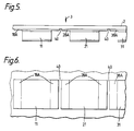
- FIGS 5 and 6 are respectively a cross-section and a plan view from the underside of part of a linear array of detectors each of the form shown in Figure 3; the three detectors shown comprise respective pyroelectric elements 11, 21 and 31 and respective resistive layers 18A, 28A and 38A, and are supported on a common flexible film 2. Each two adjacent resistive layers are separated by a respective narrow gap 40.
- the gaps may be produced by evaporation of the resistive metal through a mask, or by photolithograpy and etching of a continuous resistive coating for the complete array.
- the pyroelectric elements may each be squares of 0.5 mm side, and the resistive layers may measure 0.5 mm x 0.6 mm, i.e. an average overlap of 50 »m on each of two opposite sides of the associated pyroelectric element; the gap between adjacent resistive layers may be 20 »m wide.
- Thermal detecting means other than a pyroelectric element may be used in an embodiment of the invention, for example a dielectric element whose capacitance changes with temperature, changes in capacitance being measured.
- the flexible film 2 constitutes all the substantially transparent dielectric material preceding the detecting means, such material (whose total optical thickness is a quarter of the selected wavelength) might comprise other dielectric material as well, the thickness of the flexible film being reduced accordingly.
- a layer of other dielectric material could be vacuum-deposited on the flexible film on the side thereof remote from that on which the thermal detecting means are disposed; if this other dielectric material had a refractive index higher than that of the flexible film material, this would mean that the total physical thickness of the dielectric material would be reduced.
Landscapes
- Engineering & Computer Science (AREA)
- Power Engineering (AREA)
- Physics & Mathematics (AREA)
- General Physics & Mathematics (AREA)
- Spectroscopy & Molecular Physics (AREA)
- Photometry And Measurement Of Optical Pulse Characteristics (AREA)
- Radiation Pyrometers (AREA)
Claims (8)
- Detektor für thermische Strahlung zur Detektion von Strahlung in einem selektierten Wellenlängenbereich, aufweisend Einrichtungen, die eine temperaturabhängige Charakteristik zur Detektion thermischer Energie aufweisen, in welchem die Detektoreinrichtungen von zumindest einer flexiblen Folie getragen sind, die in diesem Wellenlängenbereich im wesentlichen transparent ist, und in welchem diese eine flexible Folie mit Bezug auf die Einfallsrichtung der zu detektierenden thermischen Strahlung den Detektoreinrichtungen vorgestellt ist,
dadurch gekennzeichnet,
daß der Detektor eine elektrische Widerstandsschicht aufweist, die einen Gesamtwirkwiderstand pro Oberflächenquadrat von im wesentlichen 377/(1+n²) Ohm pro Flächenquadrat aufweist, wobei n der Brechungsindex dieser einen flexiblen Folie ist, und die unmittelbar angrenzend an diese eine flexible Folie zwischen der flexiblen Folie und den Detektoreinrichtungen angeordnet ist, um hierdurch einfallende Strahlung in diesem Wellenlängenbereich zu absorbieren, daß die Detektoreinrichtungen thermisch mit der Widerstandsschicht gekoppelt sind und daß die optische Dicke von einem im wesentlichen transparenten dielektrischen Material, das den Detektoreinrichtungen vorgestellt ist und diese eine flexible Folie umfaßt, ein Viertel einer selektierten Wellenlänge im Wellenlängenbereich beträgt. - Detektor für thermische Strahlung zur Detektion von Strahlung in einem selektierten Wellenlängenbereich, aufweisend Einrichtungen, die eine temperaturabhängige Charakteristik zur Detektion thermischer Energie aufweisen, in welchem die Detektoreinrichtungen von zumindest einer flexiblen Folie getragen sind, die in diesem Wellenlängenbereich im wesentlichen transparent ist, und in welchem diese eine flexible Folie mit Bezug auf die Einfallsrichtung der zu detektierenden thermischen Strahlung den Detektoreinrichtungen vorgestellt ist,
dadurch gekennzeichnet,
daß der Detektor eine elektrische Widerstandsschicht aufweist, die unmittelbar angrenzend an die von den Detektoreinrichtungen abgewandte Seite dieser einen flexiblen Folie angeordnet ist und die einen Gesamtwirkwiderstand pro Flächenquadrat derart aufweist, um die einfallende Strahlung in diesem Wellenlängenbereich zu absorbieren, daß eine reflektierende, elektrisch leitende Schicht, die einfallende Strahlung im Bereich der thermischen Strahlung reflektiert, im wesentlichen in gemeinsamer Ausdehnung mit der Widerstandsschicht zwischen dieser einen flexiblen Folie und den Detektoreinrichtungen angeordnet ist, daß die Detektoreinrichtungen thermisch mit der Widerstandsschicht gekoppelt sind und daß die optische Dicke von einem im wesentlichen transparenten dielektrischen Material, das den Detektoreinrichtungen vorgestellt ist und diese eine flexible Folie umfaßt, ein Viertel einer selektierten Wellenlänge im Wellenlängenbereich beträgt. - Detektor nach Anspruch 2,
dadurch gekennzeichnet,
daß bezüglich der Einfallsrichtung zu detektierender thermischer Strahlung der Widerstandsschicht unmittelbar ein Freiraum vorgeschaltet ist und die Widerstandsschicht einen Widerstand pro Flächenquadrat im wesentlichen gleich der Kennimpedanz vom Freiraum aufweist. - Detektor nach Anspruch 1, 2 oder 3,
dadurch gekennzeichnet,
daß die optische Dicke dieser einen flexiblen Folie ein Viertel der selektierten Wellenlänge beträgt. - Detektor nach einem vorhergehenden Anspruch,
dadurch gekennzeichnet,
daß die gesamte Wärmekapazität der Schicht oder Schichten und des sich hiermit gemeinsam ausdehnenden Teils der einen flexiblen Folie sehr viel geringer als die Wärmekapazität der Detektoreinrichtungen ist. - Detektor nach einem vorhergehenden Anspruch,
dadurch gekennzeichnet,
daß die Schicht, die zwischen den Detektoreinrichtungen und dieser einen flexiblen Folie angeordnet ist, sich über im wesentlichen die Gesamtheit einer Oberfläche der Detektoreinrichtungen erstreckt, die an diese Schicht angrenzt,und im wesentlichen über zumindest einen Teil deren Umfangsbegrenzung hinaus, und durch die Wärmeenergie aus auf jeden Teil dieser Widerstandsschicht auftreffender Strahlung dieser Oberfläche der Detektoreinrichtungen zugeführt wird. - Detektor nach einem vorhergehenden Anspruch,
dadurch gekennzeichnet,
daß die Detektoreinrichtungen ein Element aus pyroelektrischem Material umfassen. - Anordnung von im wesentlichen gleichen, im wesentlichen gleichförmig beabstandeten Detektoren, jeweils nach Anspruch 6,
dadurch gekennzeichnet,
daß diese eine flexible Folie sämtlichen Detektoren gemeinsam ist, und daß in der Anordnung der Spalt zwischen den jeweiligen Schichten, die zwischen den Detektoreinrichtungen und dieser einen flexiblen Folie angeordnet sind, benachbarter Detektoren wesentlich kleiner als der Spalt zwischen den jeweiligen Detektoreinrichtungen der Detektoren ist.
Applications Claiming Priority (2)
| Application Number | Priority Date | Filing Date | Title |
|---|---|---|---|
| GB8508204 | 1985-03-29 | ||
| GB08508204A GB2173038B (en) | 1985-03-29 | 1985-03-29 | Thermal radiation detector |
Publications (3)
| Publication Number | Publication Date |
|---|---|
| EP0200241A2 EP0200241A2 (de) | 1986-11-05 |
| EP0200241A3 EP0200241A3 (en) | 1988-08-10 |
| EP0200241B1 true EP0200241B1 (de) | 1995-06-07 |
Family
ID=10576876
Family Applications (1)
| Application Number | Title | Priority Date | Filing Date |
|---|---|---|---|
| EP86200478A Expired - Lifetime EP0200241B1 (de) | 1985-03-29 | 1986-03-21 | Detektor für thermische Strahlung |
Country Status (5)
| Country | Link |
|---|---|
| US (1) | US4704534A (de) |
| EP (1) | EP0200241B1 (de) |
| JP (1) | JPH0675010B2 (de) |
| DE (1) | DE3650331T2 (de) |
| GB (1) | GB2173038B (de) |
Families Citing this family (10)
| Publication number | Priority date | Publication date | Assignee | Title |
|---|---|---|---|---|
| GB8621688D0 (en) * | 1986-09-09 | 1986-10-15 | Graviner Ltd | Radiation detection arrangements |
| GB2197753B (en) * | 1986-11-12 | 1990-01-24 | Philips Electronic Associated | Infrared radiation detection device |
| GB2198879A (en) * | 1986-12-05 | 1988-06-22 | Philips Electronic Associated | Thermal radiation detector |
| GB2202084A (en) * | 1987-03-13 | 1988-09-14 | Philips Electronic Associated | Thermal-image sensing devices and their manufacture |
| GB2206997A (en) * | 1987-07-10 | 1989-01-18 | Philips Electronic Associated | Arrays of pyroelectric or ferroelectric infrared detector elements |
| GB2236016A (en) * | 1989-09-13 | 1991-03-20 | Philips Electronic Associated | Pyroelectric and other infrared detection devices with thin films |
| DE102006010808B4 (de) * | 2006-03-07 | 2009-08-13 | BEGO Bremer Goldschlägerei Wilh. Herbst GmbH & Co. KG | Vorrichtung, System, Verfahren, Computerprogramm und Datenträger zur elektrophoretischen Abscheidung mit einer beweglichen Elektrode |
| EP2274756A1 (de) | 2008-05-08 | 2011-01-19 | Nxp B.V. | Einstellbarer kondensator |
| JP2014235146A (ja) * | 2013-06-05 | 2014-12-15 | セイコーエプソン株式会社 | テラヘルツ波検出装置、カメラ、イメージング装置および計測装置 |
| WO2018168151A1 (ja) * | 2017-03-17 | 2018-09-20 | 富士フイルム株式会社 | 焦電センサ |
Family Cites Families (8)
| Publication number | Priority date | Publication date | Assignee | Title |
|---|---|---|---|---|
| GB1508299A (en) * | 1975-06-20 | 1978-04-19 | Mullard Ltd | Pyroelectric detectors |
| JPS6015006B2 (ja) * | 1978-05-25 | 1985-04-17 | 松下電器産業株式会社 | 赤外線検出器 |
| JPS54174384U (de) * | 1978-05-30 | 1979-12-08 | ||
| GB2077034A (en) * | 1980-06-02 | 1981-12-09 | Philips Electronic Associated | Pyroelectric detector with reduced microphony |
| US4379971A (en) * | 1980-11-10 | 1983-04-12 | Statitrol, Inc. | Pyroelectric sensor |
| GB2100058B (en) * | 1981-06-05 | 1985-03-20 | Philips Electronic Associated | Pyroelectric detector |
| JPS603528A (ja) * | 1983-06-20 | 1985-01-09 | Toshiba Component Kk | 焦電形素子 |
| US4595832A (en) * | 1984-03-30 | 1986-06-17 | The United States Of America As Represented By The United States Department Of Energy | Thermal sensor with an improved coating |
-
1985
- 1985-03-29 GB GB08508204A patent/GB2173038B/en not_active Expired
-
1986
- 1986-03-03 US US06/835,709 patent/US4704534A/en not_active Expired - Lifetime
- 1986-03-21 DE DE3650331T patent/DE3650331T2/de not_active Expired - Fee Related
- 1986-03-21 EP EP86200478A patent/EP0200241B1/de not_active Expired - Lifetime
- 1986-03-26 JP JP61066080A patent/JPH0675010B2/ja not_active Expired - Lifetime
Non-Patent Citations (3)
| Title |
|---|
| Infrared Physics, vol. 14 (1974), pages 199-205 * |
| Journal of the Optical Society of America, vol. 47 (1957), pages 575-578 * |
| SPIE, vol. 380 (1983), pages 266-273 * |
Also Published As
| Publication number | Publication date |
|---|---|
| JPS61226623A (ja) | 1986-10-08 |
| GB2173038B (en) | 1988-09-14 |
| US4704534A (en) | 1987-11-03 |
| EP0200241A3 (en) | 1988-08-10 |
| JPH0675010B2 (ja) | 1994-09-21 |
| DE3650331D1 (de) | 1995-07-13 |
| GB2173038A (en) | 1986-10-01 |
| DE3650331T2 (de) | 1995-10-19 |
| EP0200241A2 (de) | 1986-11-05 |
Similar Documents
| Publication | Publication Date | Title |
|---|---|---|
| US6097031A (en) | Dual bandwith bolometer | |
| JP3597069B2 (ja) | 複数の赤外波長帯を検出する熱型赤外アレイセンサ | |
| US5424544A (en) | Inter-pixel thermal isolation for hybrid thermal detectors | |
| US6441374B1 (en) | Thermal type infrared ray detector with thermal separation structure for high sensitivity | |
| KR0135119B1 (ko) | 적외선 검출기 | |
| US2742550A (en) | Dual photoconductive infrared detector | |
| US4072864A (en) | Multilayered slant-angle thin film energy detector | |
| EP0200241B1 (de) | Detektor für thermische Strahlung | |
| US5122666A (en) | Pyroelectric and other infrared detection devices with thin films | |
| US4806763A (en) | Infrared radiation detection device | |
| US6222111B1 (en) | Spectrally selective thermopile detector | |
| EP0272731B1 (de) | Wärmestrahlungsdetektor | |
| US4469943A (en) | Pyroelectric detector | |
| US5286975A (en) | Pyro-electric type infrared-ray sensor | |
| US6429428B1 (en) | Radiation detectors | |
| US4475040A (en) | Pyroelectric infrared detector | |
| US6194721B1 (en) | Uncooled far infrared thermal imaging system | |
| US4701619A (en) | Pyroelectric detectors | |
| US20060104319A1 (en) | Device for reflecting and detecting electromagnetic radiation | |
| JPH0716016B2 (ja) | 赤外線検知素子 | |
| JP2001116616A (ja) | 熱型赤外線検出素子 | |
| JPH03146831A (ja) | 赤外検出装置 |
Legal Events
| Date | Code | Title | Description |
|---|---|---|---|
| PUAI | Public reference made under article 153(3) epc to a published international application that has entered the european phase |
Free format text: ORIGINAL CODE: 0009012 |
|
| AK | Designated contracting states |
Kind code of ref document: A2 Designated state(s): DE FR GB IT |
|
| PUAB | Information related to the publication of an a document modified or deleted |
Free format text: ORIGINAL CODE: 0009199EPPU |
|
| RA1 | Application published (corrected) |
Date of ref document: 19861210 Kind code of ref document: A2 |
|
| PUAL | Search report despatched |
Free format text: ORIGINAL CODE: 0009013 |
|
| RAP3 | Party data changed (applicant data changed or rights of an application transferred) |
Owner name: N.V. PHILIPS' GLOEILAMPENFABRIEKEN Owner name: PHILIPS ELECTRONIC AND ASSOCIATED INDUSTRIES LIMIT |
|
| AK | Designated contracting states |
Kind code of ref document: A3 Designated state(s): DE FR GB IT |
|
| 17P | Request for examination filed |
Effective date: 19890123 |
|
| 17Q | First examination report despatched |
Effective date: 19910220 |
|
| RAP3 | Party data changed (applicant data changed or rights of an application transferred) |
Owner name: N.V. PHILIPS' GLOEILAMPENFABRIEKEN Owner name: PHILIPS ELECTRONICS UK LIMITED |
|
| RAP1 | Party data changed (applicant data changed or rights of an application transferred) |
Owner name: GEC-MARCONI LIMITED |
|
| RBV | Designated contracting states (corrected) |
Designated state(s): DE FR IT |
|
| GRAA | (expected) grant |
Free format text: ORIGINAL CODE: 0009210 |
|
| AK | Designated contracting states |
Kind code of ref document: B1 Designated state(s): DE FR IT |
|
| ITF | It: translation for a ep patent filed | ||
| ET | Fr: translation filed | ||
| REF | Corresponds to: |
Ref document number: 3650331 Country of ref document: DE Date of ref document: 19950713 |
|
| PLBE | No opposition filed within time limit |
Free format text: ORIGINAL CODE: 0009261 |
|
| STAA | Information on the status of an ep patent application or granted ep patent |
Free format text: STATUS: NO OPPOSITION FILED WITHIN TIME LIMIT |
|
| PGFP | Annual fee paid to national office [announced via postgrant information from national office to epo] |
Ref country code: DE Payment date: 19960525 Year of fee payment: 11 |
|
| 26N | No opposition filed | ||
| PG25 | Lapsed in a contracting state [announced via postgrant information from national office to epo] |
Ref country code: DE Effective date: 19971202 |
|
| REG | Reference to a national code |
Ref country code: FR Ref legal event code: CD |
|
| PGFP | Annual fee paid to national office [announced via postgrant information from national office to epo] |
Ref country code: FR Payment date: 20040209 Year of fee payment: 19 |
|
| PG25 | Lapsed in a contracting state [announced via postgrant information from national office to epo] |
Ref country code: IT Free format text: LAPSE BECAUSE OF NON-PAYMENT OF DUE FEES;WARNING: LAPSES OF ITALIAN PATENTS WITH EFFECTIVE DATE BEFORE 2007 MAY HAVE OCCURRED AT ANY TIME BEFORE 2007. THE CORRECT EFFECTIVE DATE MAY BE DIFFERENT FROM THE ONE RECORDED. Effective date: 20050321 |
|
| PG25 | Lapsed in a contracting state [announced via postgrant information from national office to epo] |
Ref country code: FR Free format text: LAPSE BECAUSE OF NON-PAYMENT OF DUE FEES Effective date: 20051130 |
|
| REG | Reference to a national code |
Ref country code: FR Ref legal event code: ST Effective date: 20051130 |