EP0197475B1 - Mutiplicative scrambler and descrambler operating wordwise - Google Patents
Mutiplicative scrambler and descrambler operating wordwise Download PDFInfo
- Publication number
- EP0197475B1 EP0197475B1 EP19860104355 EP86104355A EP0197475B1 EP 0197475 B1 EP0197475 B1 EP 0197475B1 EP 19860104355 EP19860104355 EP 19860104355 EP 86104355 A EP86104355 A EP 86104355A EP 0197475 B1 EP0197475 B1 EP 0197475B1
- Authority
- EP
- European Patent Office
- Prior art keywords
- shift register
- stage
- exor
- outputs
- gate
- Prior art date
- Legal status (The legal status is an assumption and is not a legal conclusion. Google has not performed a legal analysis and makes no representation as to the accuracy of the status listed.)
- Expired - Lifetime
Links
Images

Classifications
-
- H—ELECTRICITY
- H03—ELECTRONIC CIRCUITRY
- H03M—CODING; DECODING; CODE CONVERSION IN GENERAL
- H03M5/00—Conversion of the form of the representation of individual digits
- H03M5/02—Conversion to or from representation by pulses
- H03M5/04—Conversion to or from representation by pulses the pulses having two levels
- H03M5/14—Code representation, e.g. transition, for a given bit cell depending on the information in one or more adjacent bit cells, e.g. delay modulation code, double density code
- H03M5/145—Conversion to or from block codes or representations thereof
-
- H—ELECTRICITY
- H04—ELECTRIC COMMUNICATION TECHNIQUE
- H04L—TRANSMISSION OF DIGITAL INFORMATION, e.g. TELEGRAPHIC COMMUNICATION
- H04L25/00—Baseband systems
- H04L25/02—Details ; arrangements for supplying electrical power along data transmission lines
- H04L25/03—Shaping networks in transmitter or receiver, e.g. adaptive shaping networks
- H04L25/03828—Arrangements for spectral shaping; Arrangements for providing signals with specified spectral properties
- H04L25/03866—Arrangements for spectral shaping; Arrangements for providing signals with specified spectral properties using scrambling
- H04L25/03872—Parallel scrambling or descrambling
-
- H—ELECTRICITY
- H04—ELECTRIC COMMUNICATION TECHNIQUE
- H04L—TRANSMISSION OF DIGITAL INFORMATION, e.g. TELEGRAPHIC COMMUNICATION
- H04L25/00—Baseband systems
- H04L25/38—Synchronous or start-stop systems, e.g. for Baudot code
- H04L25/40—Transmitting circuits; Receiving circuits
- H04L25/49—Transmitting circuits; Receiving circuits using code conversion at the transmitter; using predistortion; using insertion of idle bits for obtaining a desired frequency spectrum; using three or more amplitude levels ; Baseband coding techniques specific to data transmission systems
- H04L25/4906—Transmitting circuits; Receiving circuits using code conversion at the transmitter; using predistortion; using insertion of idle bits for obtaining a desired frequency spectrum; using three or more amplitude levels ; Baseband coding techniques specific to data transmission systems using binary codes
- H04L25/4908—Transmitting circuits; Receiving circuits using code conversion at the transmitter; using predistortion; using insertion of idle bits for obtaining a desired frequency spectrum; using three or more amplitude levels ; Baseband coding techniques specific to data transmission systems using binary codes using mBnB codes
Definitions
- the invention relates to a word-by-word, multiplicative scrambler or descrambler for m-bit-wide data words according to the preamble of claim 1 or 2.
- Such scramblers or scramblers are known, for example by the essay "Realization of scramblers for PCM signals high clock frequency "by Mauchmann, Siemens Research and Development Report Volume 6 of 1977 No. 1 Pages 1 to 5.
- the principle of the multiplicative scrambler or descrambler can be derived from the above-mentioned article, a feedback shift register being used to generate quasi-random sequences which are linked to the data bit sequence to be scrambled or descrambled.
- serial scrambler or descrambler At high transmission rates or step speeds, the realization of a serial scrambler or descrambler becomes critical. In the same article, it was therefore proposed to split the serial data signal with a high clock frequency into several partial data streams, which are then fed to a parallelized scrambler or descrambler.
- serial-parallel conversion of a scambler or descrambler structure requires extensive computing work, and the effort of the recursive network to be implemented is relatively high.
- the object of the present invention was therefore to find a scrambler or descrambler structure which enables operation even at very high clock frequencies and involves less effort for implementation. These Structure should be able to meet the high demands placed on modern scramblers and descramblers, which are listed below.
- the scrambler or descrambler according to the invention has the advantage of ensuring, with little effort for the implementation, the synchronization of the reception decoder of a line transmission device even at high step speeds and when transmitting periodic signals. In addition, the self-test of the encoder and decoder of a transmission link is made possible.
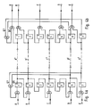
- FIG. 3 shows a general scrambler-descrambler structure for using the method according to the invention.
- FIG. 3a shows the scrambler and
- FIG. 3b shows the descrambler, a shift register with n stages being recognizable in each case, which has two returns QR1 and QR2.
- a mod-2 adder is inserted before the input of a stage, at whose second input one of the m parallel data signals is present. If m ⁇ n, nm stages of the shift register are only used with the shift function. The relevant mod-2 adder is then bridged, see dashed line in Fig. 3a and 3b at the second stage.
- 3b also contains a shift register, but the forward coupling between the individual stages is separated and replaced by a mod-2 adder in such a way that the output of the previous stage and the input of the next stage are linked to mod-2 one of the m parallel signals at the output of the mod-2 adder.
- the feedback in the descrambler has to be done in exactly the same way as with the scrambler. Only then is it guaranteed that the scrambled parallel signals Ai, Aj, ... Am are converted back into m parallel signals Ei, Ej, ... Em, which correspond to the input signals of the scrambler.
- 3a and 3b are selected for the transmission of this signal via optical waveguide transmission systems. Since a 5 or 6-stage scrambler cannot generate all possible values in the code table at the code output if a signal with a permanent position is present at the data inputs of the srambler, n must be selected at least equal to 7.
- Tables 1 and 2 show a list of the different possible feedbacks of a 7-stage scrambler of maximum length and a list of the different possibilities of data management A, B, C, D and E in order to meet the requirements for a 5B6B code according to the European patent application 64 097 to be met if a data signal with permanent position 1 (table 1) or permanent position 0 (table 2) is present at the scrambler input.
- Table 2 it should be noted that a corresponding descrambler structure according to FIG. 3b is not possible for the scrambler structure according to line 1.
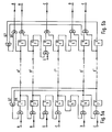
- the parallelized input signals A to E are fed to stages 1, 2, 4, 6 and 7, at whose outputs the scrambled parallel signals A ', B', ... E 'are present.
- the feedback takes place from the 6th and the 7th stage to the input of the 1st stage.
- the descrambling takes place in the corresponding manner, this structure is shown in FIG. 4b.
- FIG. 5 shows a further embodiment of the invention. It shows the same structure as in FIG. 4. In addition, however, monitoring is provided to prevent the scrambler from delivering a periodic output signal.
- the scrambler is in such a permanent position when there is 0 at the data inputs with the scrambler content 0000000 in the case of a permanent position and 0110010 at the data inputs with the permanent position 1. In order to exclude these permanent positions, the scrambler contents are decoded to the values mentioned. If one of these two 7-bit words is recognized, a scrambler bit is inverted. It is particularly favorable to invert the 3rd or 5th scrambler bit, since no additional gate level is required. In FIG.
- an inversion of the 3rd scrambler stage was provided, a mod-2 adder being inserted in the scrambler at the input of the 3rd stage, the inverting monitoring signal U being present at its 2nd input.
- a corresponding measure is provided in the descrambler according to FIG. 5b.
Description
Die Erfindung bezieht sich auf einen wortweise arbeitenden, multiplikativen Verwürfler bzw. Entwürfler für m-Bit-breite Datenworte gemäß Oberbegriff des Patentanspruchs 1 bzw. 2. Solche Verwürfler bzw. Entwürfler sind bekannt, beispielsweise durch den Aufsatz "Realisierung von Scramblern für PCM-Signale hoher Taktfrequenz" von Möhrmann, Siemens Forschungs- und Entwicklungsbericht Band 6 von 1977 Nr. 1 Seiten 1 bis 5.
Aus dem genannten Aufsatz ist das Prinzip des multiplikativen Scramblers bzw. Descramblers entnehmbar, wobei ein rückgekoppeltes Schieberegister benutzt wird, um Quasi-Zufallsfolgen zu erzeugen, welche mit der zu verwürfelnden bzw. zu entwürfelnden Datenbitfolge verknüpft werden.
Bei hohen Übertragungsraten bzw. Schrittgeschwindigkeiten wird die Realisierung eines seriellen Scramblers bzw. Descramblers kritisch. Im selben Aufsatz ist deshalb vorgeschlagen worden, das serielle Datensignal hoher Taktfrequenz aufzuteilen in mehrere Teildatenströme, die dann einem parallelisierten Scrambler bzw. Descrambler zugeführt werden.The invention relates to a word-by-word, multiplicative scrambler or descrambler for m-bit-wide data words according to the preamble of
The principle of the multiplicative scrambler or descrambler can be derived from the above-mentioned article, a feedback shift register being used to generate quasi-random sequences which are linked to the data bit sequence to be scrambled or descrambled.
At high transmission rates or step speeds, the realization of a serial scrambler or descrambler becomes critical. In the same article, it was therefore proposed to split the serial data signal with a high clock frequency into several partial data streams, which are then fed to a parallelized scrambler or descrambler.
Die Serien-Parallel-Umwandlung einer Scambler- bzw. Descrambler-Struktur erfordert eine umfangreiche Rechenarbeit, und der Aufwand des zu realisierenden rekursiven Netzwerkes ist relativ hoch.The serial-parallel conversion of a scambler or descrambler structure requires extensive computing work, and the effort of the recursive network to be implemented is relatively high.
Aufgabe der vorliegenden Erfindung war es deshalb, eine Scrambler- bzw. Descrambler-Struktur zu finden, die einen Betrieb auch bei sehr hohen Taktfrequenzen ermöglicht und weniger Aufwand für die Realisierung mit sich bringt. Diese Struktur sollte in der Lage sein, die an moderne Scrambler und Descrambler gestellten hohen Anforderungen, die weiter unten aufgelistet werden, zu erfüllen.The object of the present invention was therefore to find a scrambler or descrambler structure which enables operation even at very high clock frequencies and involves less effort for implementation. These Structure should be able to meet the high demands placed on modern scramblers and descramblers, which are listed below.
Diese Aufgabe wird durch den erfindungsgemäßen Verwürfler und Entwürfler nach Anspruch 1 bzw. 2 gelöst. Optimale Ausgestaltungen ergeben sich durch die Unteransprüche.This object is achieved by the scrambler and descrambler according to the invention. Optimal designs result from the subclaims.
Der erfindungsgemäße Verwürfler bzw. Entwürfler hat den Vorteil, bei wenig Aufwand für die Realisierung die Synchronisation des Empfangsdecoders einer Leitungsübertragungseinrichtung auch bei hohen Schrittgeschwindigkeiten und bei Übertragung von periodischen Signalen zu gewährleisten. Außerdem wird der Selbsttest von Coder und Decoder einer Übertragungsstrecke ermöglicht.The scrambler or descrambler according to the invention has the advantage of ensuring, with little effort for the implementation, the synchronization of the reception decoder of a line transmission device even at high step speeds and when transmitting periodic signals. In addition, the self-test of the encoder and decoder of a transmission link is made possible.
In dem Aufsatz "Parallel arbeitende Scrambler Descrambler und Zufallsfolgegeneratoren" in ELEKTRONIK Band 32 Nr. 26 Dez. 1983, Seiten 67 bis 70, sind multiplikative Verwürfler (Bild 4) bzw. Entwürfler (Bild 6) maximaler Länge bekanntgeworden, die einige Merkmale gemäß Oberbegriff Patentanspruch 1 bzw. 2 aber auch jeweils eine doppelte Kopplung der Schieberegisterstufen und über zwei Gatterebenen aufweisen. Dies hat die Nachteile eines mehrfachen Aufwandes für Logikschaltung und Verdrahtung sowie, daß die zweifachen Gatterebenen eine zusätzliche Laufzeit bedingen, wodurch die maximale Taktfrequenz, mit der die Schaltungen noch arbeiten können, stark begrenzt ist.In the essay "Parallel Scrambler Descrambler and Random Sequence Generators" in ELEKTRONIK Volume 32 No. 26 Dec. 1983, pages 67 to 70, multiplicative scramblers (Fig. 4) and descramblers (Fig. 6) of maximum length have become known, some features according to the
Es folgt nun die Beschreibung der Erfindung anhand der Figuren.
In digitalen Übertragungssystemen großer Übertragungskapazität kommt der Überwachung der Übertragungsstrecke im laufenden Betrieb besondere Bedeutung zu. Mit Hilfe von redundanten Leitungscodes ist eine derartige Überwachung möglich. Darüber hinaus kann durch geeignete Wahl des Codes die Übertragungsqualität verbessert werden. Die Figur 1 zeigt die prinzipielle Anordnung von Coder und Decoder bei einem Lichtwellenleiter-Übertragungssystem. Für die Übertragung über Lichtwellenleiter werden Blockcodes mit begrenzter laufenden digitalen Summe (LDS) eingesetzt. Fehler bei der Übertragung führen zum Überschreiten der Grenzen der LDS. Damit ist eine einfache Möglichkeit zur Fehlererkennung während des Betriebs gegeben. In der optischen Übertragungstechnik wird für die Leitungscodierung im allgemeinen ein 5B6B-Code mit einer begrenzten laufenden digitalen Summe von ±3 verwendet.
Bei der Übertragung von periodischen Signalen wie z.B. dem "Alarm Inhibit Signal" (AIS) treten Probleme bei der Synchronisation des Decoders auf. Bei bestimmten periodischen Signalen ist eine sichere Synchronisation des Decoders nicht gewährleistet, weshalb weitere Maßnahmen ergriffen werden müssen.
Die Figur 2 zeigt, wie vor dem Coder ein Verwürfler (Scrambler) und auf der Empfangsseite nach dem Decoder ein entsprechender Entwürfler (Descrambler) eingefügt ist. Ein solcher Verwürfler hat die Aufgabe, das anfallende Datensignal in ein zufallsähnliches Signal zu überführen, wobei folgende Forderungen gestellt werden müssen.
- 1. Durch den Scrambler soll eine Datenfolge angeboten werden, die nach der Codierung möglichst viele 1-0-Übergänge erzeugt, so daß eine günstige Taktableitung und eine gute Synchronisation ermöglicht werden.
- 2. Durch den Scrambler soll dem Coder ein Datensignal mit einer möglichst statistischen Folge auch dann angeboten werden, wenn am Scramblereingang das Dateneingangssignal mit Dauerlage ansteht.
- 3. Wenn am Dateneingang des Scramblers ein Datensignal mit einer bestimmten Dauerlage ansteht, so muß der Scrambler eine Datenfolge liefern, durch die am Coderausgang die vollständige Codetabelle erzeugt wird, dadurch ist eine vollständige Überprüfung im Selbsttest des Coders und des Decoders einschließlich der Synchronisation möglich.
- 4. Bei Nicht-Synchronisation des Decoders müssen möglichst viele Codeverletzungen erzeugt werden.
- 5. Im allgemeinen sind diese Anforderungen nur mit einem Verwürfler erreichbar, der über ein n-stufiges Schieberegister verfügt, welches derart rückgekoppelt ist, daß eine Quasi-Zufallsfolge mit maximaler Länge erzeugt wird.
In digital transmission systems with a large transmission capacity, monitoring the transmission link during operation is of particular importance. Such monitoring is possible with the help of redundant line codes. In addition, the transmission quality can be improved by a suitable choice of the code. Figure 1 shows the basic arrangement of encoder and decoder in an optical fiber transmission system. Block codes with limited running digital sum (LDS) are used for the transmission via fiber optic cables. Transmission errors lead to the limits of the LDS being exceeded. This provides an easy way to identify errors during operation. In optical transmission technology, a 5B6B code with a limited running digital sum is generally used for line coding used by ± 3.
When periodic signals such as the "Alarm Inhibit Signal" (AIS) are transmitted, problems occur when the decoder is synchronized. With certain periodic signals, reliable synchronization of the decoder is not guaranteed, which is why further measures must be taken.
FIG. 2 shows how a scrambler is inserted in front of the coder and a corresponding descrambler on the reception side after the decoder. Such a scrambler has the task of converting the resulting data signal into a randomly similar signal, the following requirements having to be made.
- 1. The scrambler is intended to offer a data sequence which, after coding, generates as many 1-0 transitions as possible, so that favorable clock derivation and good synchronization are made possible.
- 2. The scrambler is intended to offer the coder a data signal with a statistical sequence as possible, even if the data input signal with permanent position is present at the scrambler input.
- 3. If a data signal with a certain permanent position is present at the data input of the scrambler, the scrambler must supply a data sequence by which the complete code table is generated at the coder output. This enables a complete check in the self-test of the encoder and decoder, including the synchronization.
- 4. If the decoder is not synchronized, as many code violations as possible must be generated.
- 5. In general, these requirements can only be achieved with a scrambler that has an n-stage shift register, which is fed back in such a way that a quasi-random sequence of maximum length is generated.
Die Figur 3 zeigt eine allgemeine Scrambler-Descramblerstruktur zur Anwendung des erfindungsgemäßen Verfahrens. Die Figur 3a zeigt den Scrambler und die Figur 3b den Descrambler, wobei jeweils ein Schieberegister mit n Stufen erkennbar ist, welches über 2 Rückführungen QR1 und QR2 verfügt. Vor dem Eingang einer Stufe ist jeweils ein mod-2-Addierer eingefügt, an dessen zweitem Eingang eines der m parallelen Datensignale anliegt. Falls m < n ist, werden n-m Stufen des Schieberegisters lediglich mit der Funktion Schieben benutzt. Das betreffende mod-2-Addierglied wird dann überbrückt, siehe gestrichelte Linie in Fig. 3a und 3b bei der zweiten Stufe.
Auch der Descrambler nach Fig. 3b enthält ein Schieberegister, wobei jedoch die Vorwärts-Kopplung zwischen den einzelnen Stufen aufgetrennt und durch ein mod-2-Addierer derart ersetzt wird, daß Ausgang der vorhergehenden Stufe und Eingang der nächsten Stufe mod-2 verknüpft werden zu einem der m parallelen Signale am Ausgang des mod-2-Addierers. Es ist selbstverständlich, daß die Rückkopplung im Descrambler in genau der gleichen Weise zu erfolgen hat wie beim Scrambler. Nur dann ist gewährleistet, daß die verwürfelten parallelen Signale Ai, Aj, ... Am wieder in m parallele Signale Ei, Ej, ... Em zurückgewandelt werden, die den Eingangssignalen des Scramblers entsprechen.
Neben der hohen Verträglichkeit dieser Verwürfler-Struktur bezüglich hoher Schrittgeschwindigkeiten und der Selbstsynchronisationsfähigkeit besteht ein weiterer Vorteil darin, daß durch Vertauschen der Eingangssignale, durch Vergrößern der Stufenzahl und durch verschiedene Möglichkeiten der Rückkopplungen QR1 und QR2 viele Freiheitsgrade ermöglicht werden.
Diese Freiheitsgrade ermöglichen wiederum, spezielle Anforderungen an einen Scrambler zu stellen und zu realisieren. Der in Lichtwellenleiter-Übertragungssystemen verwendete 5B6B-Code hat die Eigenschaft, daß es viele periodische Folgen und Dauerlagen gibt, die auf der Decoderseite keine Synchronisation ermöglichen. Zu diesen Dauerlagen gehört auch die Dauerlage 1, welche das AIS-Signal darstellt. Zur Übertragung dieses Signals über Lichtwellenleiter-Übertragungssysteme werden die Verwürfler-Struktur nach Figur 4a und die Entwürfler-Struktur nach Figur 4b, welche eine Ausgestaltung der allgemeineren Struktur nach den Figuren 3a und 3b darstellt, ausgewählt. Da mit einem 5- oder 6-stufigen Scrambler am Code-Ausgang nicht alle möglichen Werte der Code-Tabelle erzeugt werden können, wenn an den Dateneingängen des Sramblers ein Signal mit Dauerlage ansteht, muß n zumindestens gleich 7 gewählt werden.
Die Tabellen 1 und 2 zeigen eine Auflistung der verschiedenen möglichen Rückkopplungen eines 7-stufigen Scramblers maximaler Länge und eine Auflistung der verschiedenen Möglichkeiten der Datenführung A, B, C, D und E, um die gestellten Anforderungen für einen 5B6B-Code nach der europäischen Patentanmeldung 64 097 zu erfüllen, wenn am Scramblereingang ein Datensignal mit der Dauerlage 1 (Tabelle 1) bzw. Dauerlage 0 (Tabelle 2) ansteht. In Ergänzung zur Tabelle 2 ist festzustellen, daß zu der Scrambler-Stuktur gemäß Zeile 1 ein entsprechender Descrambler-Aufbau gemäß Figur 3b nicht möglich ist.FIG. 3 shows a general scrambler-descrambler structure for using the method according to the invention. FIG. 3a shows the scrambler and FIG. 3b shows the descrambler, a shift register with n stages being recognizable in each case, which has two returns QR1 and QR2. A mod-2 adder is inserted before the input of a stage, at whose second input one of the m parallel data signals is present. If m <n, nm stages of the shift register are only used with the shift function. The relevant mod-2 adder is then bridged, see dashed line in Fig. 3a and 3b at the second stage.
The descrambler according to FIG. 3b also contains a shift register, but the forward coupling between the individual stages is separated and replaced by a mod-2 adder in such a way that the output of the previous stage and the input of the next stage are linked to mod-2 one of the m parallel signals at the output of the mod-2 adder. It goes without saying that the feedback in the descrambler has to be done in exactly the same way as with the scrambler. Only then is it guaranteed that the scrambled parallel signals Ai, Aj, ... Am are converted back into m parallel signals Ei, Ej, ... Em, which correspond to the input signals of the scrambler.
In addition to the high compatibility of this scrambler structure with regard to high step speeds and the ability to self-synchronize, there is a further advantage that many degrees of freedom are made possible by interchanging the input signals, increasing the number of stages and using various possibilities of the QR1 and QR2 feedbacks.
These degrees of freedom in turn make it possible to place and implement special requirements for a scrambler. The one used in fiber optic transmission systems 5B6B code has the property that there are many periodic sequences and permanent positions that do not allow synchronization on the decoder side. These permanent positions also include
Tables 1 and 2 show a list of the different possible feedbacks of a 7-stage scrambler of maximum length and a list of the different possibilities of data management A, B, C, D and E in order to meet the requirements for a 5B6B code according to the European patent application 64 097 to be met if a data signal with permanent position 1 (table 1) or permanent position 0 (table 2) is present at the scrambler input. In addition to Table 2, it should be noted that a corresponding descrambler structure according to FIG. 3b is not possible for the scrambler structure according to
Beim Scrambler nach Figur 4a werden die parallelisierten Eingangssignale A bis E den Stufen 1, 2, 4, 6 und 7 zugeführt, an deren Ausgängen die verwürfelten parallelen Signale A', B', ... E' anstehen. Die Rückkopplung erfolgt von der 6. und der 7. Stufe auf den Eingang der 1. Stufe. Die Entwürfelung erfolgt in der entsprechenden Weise, diese Struktur ist in Figur 4b gezeichnet.In the scrambler according to FIG. 4a, the parallelized input signals A to E are fed to
Eine weitere Ausgestaltung der Erfindung zeigt die Figur 5. Sie zeigt dieselbe Stuktur wie nach Figur 4. Zusätzlich ist jedoch eine Überwachung vorgesehen, die verhindern soll, daß der Scrambler ein periodisches Ausgangssignal liefert. In einer solchen Dauerlage befindet sich der Scrambler dann, wenn bei einer Dauerlage 0 an den Dateneingängen mit dem Scramblerinhalt 0000000 und bei der Dauerlage 1 an den Dateneingängen mit dem Scramblerinhalt 0110010 ansteht. Um diese Dauerlagen auszuschließen, werden die Scramblerinhalte auf die genannten Werte decodiert. Wird eines dieser beiden 7-Bit-Worte erkannt, so wird ein Scrambler-Bit invertiert. Besonders günstig ist es, das 3. oder das 5. Scrambler-Bit zu invertieren, da hierbei keine zusätzliche Gatterebene erforderlich ist.
In Figur 5 wurde jeweils eine Inversion der 3. Scrambler-Stufe vorgesehen, wobei im Scrambler am Eingang der 3. Stufe ein mod-2-Addierer eingefügt ist, an dessen 2. Eingang das invertierende Überwachungssignal Ü anliegt. Eine entsprechende Maßnahme ist im Descrambler nach Figur 5b vorgesehen.


In FIG. 5, an inversion of the 3rd scrambler stage was provided, a mod-2 adder being inserted in the scrambler at the input of the 3rd stage, the inverting monitoring signal U being present at its 2nd input. A corresponding measure is provided in the descrambler according to FIG. 5b.
Claims (5)
- Multiplication scrambler operating in parallel mode word by word for data words having a width of m bits, with an n-stage shift register which is provided with feedback and connected behind a single EXOR stage having a width of m gates for the parallel interlinking of the respective data word with the shift register content, wherein n is at least equal to m, wherein the first data bit (Ei) and the output of a further EXOR gate, to the inputs of which the outputs (QR1, QR2) of at least two stages are led for the feedback of the shift register (stages 1, 2, 3 ... n), are present at the first gate of the EXOR stage, characterised thereby, that the respective following data bit (Ej, Ek, E1 ... Em) and the output of the respective preceding shift register stage (1, 2, 3 ... n-1) are present at the following gates of the EXOR stage and that the scrambled data word having a width of m bits (Ai, Aj, Ak, Al ... Am) is present at the outputs of the shift register stages (1, 2, 3, 4 ... n), the inputs of which are respectively connected with the m gate outputs of the EXOR stage or with the outputs of the preceding shift register stages (Figure 3a).
- Multiplicative unscrambler operating in parallel mode word by word for scrambled data words having a width of m bits, with an n-stage shift register which is provided with feedback and connected in front of a single EXOR stage having a width of m gates for the parallel interlinking of the respective scrambled data word with the shift register content, wherein m is at most equal to n, wherein the first data bit (Ai) and the output of a further EXOR gate, at the inputs of which the outputs (QR1, QR2) of at least two shift register stages are present as feedback, are present at the first gate of the EXOR stage, characterised thereby, that the respective following data bit (Aj, Ak .,. Am) and the output of the respective preceding shift register stage are present at the following gates of the EXOR stage, that the individual bits (Ai, Aj, Ak ... Am) of the scrambled data word are each applied to respective inputs of m shift register stages (1, 2, 3 ... m), that each output of a shift register stage not applied to a gate of the EXOR stage is connected with the input of the following shift register stage and that the individual bits (Ei, Ej, Ek ... Em) of the unscrambled data word are present at the outputs of the EXOR stage (Figure 3b).
- Scrambler according to claim 1, characterised thereby, that m is equal to 5 and n is equal to 7, that the outputs (Q6, Q7) of the sixth and seventh shift register stages are led to the inputs of the further EXOR gate and that the gate outputs of the EXOR stage are connected with the inputs of the first, second, fourth , sixth and seventh shift register stages (Figure 4a).
- Unscrambler according to claim 2, characterised thereby, that m is equal to 5 and n is equal to 7, that the outputs of the sixth and seventh shift register stages (Q6, Q7) are led to the inputs of the further EXOR gate and that the outputs (Q1, Q2, Q4, Q6, Q7) of the first, second, fourth, sixth and seventh shift register stages are connected with the gates of the EXOR stage (Figure 4b).
- Circuit arrangement according to claim 3 or 4, characterised thereby, that the input of one of the shift register stages (3), with which no data bit is associated, is connected with the output of an additional EXOR gate, to the two inputs of which is applied the output of the preceding shift register stage (2) and a monitoring signal (Ü), the level of which causes an inversion of the bit (Q3) present in the case of a shift register content of 0 00 00 00 or 0 11 00 10 (Figures 5a and 5b).
Applications Claiming Priority (2)
| Application Number | Priority Date | Filing Date | Title |
|---|---|---|---|
| DE19853512126 DE3512126C1 (en) | 1985-04-03 | 1985-04-03 | Word-wise working, multiplicative caster and designer |
| DE3512126 | 1985-04-03 |
Publications (3)
| Publication Number | Publication Date |
|---|---|
| EP0197475A2 EP0197475A2 (en) | 1986-10-15 |
| EP0197475A3 EP0197475A3 (en) | 1988-09-21 |
| EP0197475B1 true EP0197475B1 (en) | 1992-05-27 |
Family
ID=6267168
Family Applications (1)
| Application Number | Title | Priority Date | Filing Date |
|---|---|---|---|
| EP19860104355 Expired - Lifetime EP0197475B1 (en) | 1985-04-03 | 1986-03-29 | Mutiplicative scrambler and descrambler operating wordwise |
Country Status (2)
| Country | Link |
|---|---|
| EP (1) | EP0197475B1 (en) |
| DE (1) | DE3512126C1 (en) |
Families Citing this family (2)
| Publication number | Priority date | Publication date | Assignee | Title |
|---|---|---|---|---|
| US4791653A (en) * | 1987-08-25 | 1988-12-13 | Hewlett-Packard Company | Pseudorandom word sequence synchronizer |
| US5307409A (en) * | 1992-12-22 | 1994-04-26 | Honeywell Inc | Apparatus and method for fault detection on redundant signal lines via encryption |
Family Cites Families (4)
| Publication number | Priority date | Publication date | Assignee | Title |
|---|---|---|---|---|
| DE2634353C2 (en) * | 1976-07-30 | 1978-08-31 | Siemens Ag, 1000 Berlin Und 8000 Muenchen | Message transmission system for pulse code modulation with scrambler on the sending side and synchronized descrambler on the receiving side |
| GB1591805A (en) * | 1978-01-12 | 1981-06-24 | Gen Electric Co Ltd | Electric signal generators |
| DE3403639A1 (en) * | 1984-02-02 | 1985-08-08 | Siemens AG, 1000 Berlin und 8000 München | SELF-SYNCHRONIZING DESIGNER |
| DE3403650A1 (en) * | 1984-02-02 | 1985-08-08 | Siemens AG, 1000 Berlin und 8000 München | SELF-SYNCHRONIZING SCRAMBLER |
-
1985
- 1985-04-03 DE DE19853512126 patent/DE3512126C1/en not_active Expired
-
1986
- 1986-03-29 EP EP19860104355 patent/EP0197475B1/en not_active Expired - Lifetime
Also Published As
| Publication number | Publication date |
|---|---|
| DE3512126C1 (en) | 1986-08-14 |
| EP0197475A2 (en) | 1986-10-15 |
| EP0197475A3 (en) | 1988-09-21 |
Similar Documents
| Publication | Publication Date | Title |
|---|---|---|
| DE1537062A1 (en) | Key generator | |
| EP0553648A1 (en) | Parallel scrambler and descrambler | |
| DE4308241A1 (en) | ||
| DE3403650C2 (en) | ||
| DE3420801C2 (en) | ||
| DE2712974B1 (en) | Circuit arrangement for generating signals in the code-mark inversion code | |
| EP0197475B1 (en) | Mutiplicative scrambler and descrambler operating wordwise | |
| EP0173842A2 (en) | Self-synchronizing descrambler | |
| DE2753999C3 (en) | Digital time division multiplex transmission system | |
| EP0150861B1 (en) | Self-synchronizing descrambler | |
| DE1934869B2 (en) | PROCEDURE AND CIRCUIT ARRANGEMENT FOR CODING ASYNCHRONOUS BINARY DIGITAL SIGNALS | |
| DE3042394C2 (en) | ||
| DE3031579C2 (en) | CMI encoder | |
| DE4223639C1 (en) | Transmission system for 2 independent digital signals - uses encoder supplied with digital signals at pulse channel and signal channel respectively | |
| DE2634353C2 (en) | Message transmission system for pulse code modulation with scrambler on the sending side and synchronized descrambler on the receiving side | |
| DE2633516C3 (en) | Digital messaging system | |
| DE3526052A1 (en) | Digital communication system with an nB/(n+1)B line code | |
| EP0136663A2 (en) | AMI coded signal transmission system | |
| DE4205623B4 (en) | line terminal | |
| DE2647716B1 (en) | Path section monitor for PCM TDMA system - replaces first frame identification word with second word during alarm indication | |
| DE2944377A1 (en) | JITTER REDUCTION IN BLOCK RECODING OF DIGITAL SIGNALS | |
| EP0038509A1 (en) | Logic circuit to avoid a latch-up condition between distant data buses | |
| DE3701926B3 (en) | A method of forming a pseudorandom bit string in a digital speech encryption device | |
| DE1537949A1 (en) | Circuit arrangement for the encryption and decryption of messages transmitted in pulses | |
| DE2430760A1 (en) | Coding device with transmitter coder and receiver decoder - has two shift registers, one with five and other with four d-flip-flops |
Legal Events
| Date | Code | Title | Description |
|---|---|---|---|
| PUAI | Public reference made under article 153(3) epc to a published international application that has entered the european phase |
Free format text: ORIGINAL CODE: 0009012 |
|
| AK | Designated contracting states |
Kind code of ref document: A2 Designated state(s): FR GB IT |
|
| PUAL | Search report despatched |
Free format text: ORIGINAL CODE: 0009013 |
|
| AK | Designated contracting states |
Kind code of ref document: A3 Designated state(s): FR GB IT |
|
| 17P | Request for examination filed |
Effective date: 19890223 |
|
| 17Q | First examination report despatched |
Effective date: 19910319 |
|
| GRAA | (expected) grant |
Free format text: ORIGINAL CODE: 0009210 |
|
| ITF | It: translation for a ep patent filed |
Owner name: BARZANO' E ZANARDO MILANO S.P.A. |
|
| AK | Designated contracting states |
Kind code of ref document: B1 Designated state(s): FR GB IT |
|
| ET | Fr: translation filed | ||
| GBT | Gb: translation of ep patent filed (gb section 77(6)(a)/1977) | ||
| PLBE | No opposition filed within time limit |
Free format text: ORIGINAL CODE: 0009261 |
|
| STAA | Information on the status of an ep patent application or granted ep patent |
Free format text: STATUS: NO OPPOSITION FILED WITHIN TIME LIMIT |
|
| 26N | No opposition filed | ||
| PGFP | Annual fee paid to national office [announced via postgrant information from national office to epo] |
Ref country code: GB Payment date: 19950307 Year of fee payment: 10 |
|
| PGFP | Annual fee paid to national office [announced via postgrant information from national office to epo] |
Ref country code: FR Payment date: 19950316 Year of fee payment: 10 |
|
| PG25 | Lapsed in a contracting state [announced via postgrant information from national office to epo] |
Ref country code: GB Effective date: 19960329 |
|
| GBPC | Gb: european patent ceased through non-payment of renewal fee |
Effective date: 19960329 |
|
| PG25 | Lapsed in a contracting state [announced via postgrant information from national office to epo] |
Ref country code: FR Effective date: 19961129 |
|
| REG | Reference to a national code |
Ref country code: FR Ref legal event code: ST |
|
| PG25 | Lapsed in a contracting state [announced via postgrant information from national office to epo] |
Ref country code: IT Free format text: LAPSE BECAUSE OF NON-PAYMENT OF DUE FEES Effective date: 20050329 |