EP0193315B1 - Method and apparatus for examining a workpiece - Google Patents
Method and apparatus for examining a workpiece Download PDFInfo
- Publication number
- EP0193315B1 EP0193315B1 EP86301008A EP86301008A EP0193315B1 EP 0193315 B1 EP0193315 B1 EP 0193315B1 EP 86301008 A EP86301008 A EP 86301008A EP 86301008 A EP86301008 A EP 86301008A EP 0193315 B1 EP0193315 B1 EP 0193315B1
- Authority
- EP
- European Patent Office
- Prior art keywords
- workpiece
- signal
- flaw
- coil
- signals
- Prior art date
- Legal status (The legal status is an assumption and is not a legal conclusion. Google has not performed a legal analysis and makes no representation as to the accuracy of the status listed.)
- Expired - Lifetime
Links
- 238000000034 method Methods 0.000 title claims description 10
- 238000012360 testing method Methods 0.000 claims abstract description 39
- 238000003384 imaging method Methods 0.000 claims abstract description 9
- 230000005672 electromagnetic field Effects 0.000 claims description 5
- 238000012544 monitoring process Methods 0.000 claims description 5
- 230000004048 modification Effects 0.000 claims description 4
- 238000012986 modification Methods 0.000 claims description 4
- 230000008878 coupling Effects 0.000 claims description 3
- 238000010168 coupling process Methods 0.000 claims description 3
- 238000005859 coupling reaction Methods 0.000 claims description 3
- 230000001939 inductive effect Effects 0.000 abstract description 2
- 238000001514 detection method Methods 0.000 description 9
- 239000000523 sample Substances 0.000 description 7
- 239000003990 capacitor Substances 0.000 description 5
- 230000007547 defect Effects 0.000 description 5
- 230000010363 phase shift Effects 0.000 description 5
- 229910000831 Steel Inorganic materials 0.000 description 3
- 239000000463 material Substances 0.000 description 3
- 239000002184 metal Substances 0.000 description 3
- 230000004044 response Effects 0.000 description 3
- 239000010959 steel Substances 0.000 description 3
- 230000001360 synchronised effect Effects 0.000 description 3
- 230000005540 biological transmission Effects 0.000 description 2
- 238000011161 development Methods 0.000 description 2
- 230000005670 electromagnetic radiation Effects 0.000 description 2
- 238000004519 manufacturing process Methods 0.000 description 2
- 230000035945 sensitivity Effects 0.000 description 2
- 238000007493 shaping process Methods 0.000 description 2
- 230000004075 alteration Effects 0.000 description 1
- 239000004020 conductor Substances 0.000 description 1
- 230000003247 decreasing effect Effects 0.000 description 1
- 230000001934 delay Effects 0.000 description 1
- 230000003111 delayed effect Effects 0.000 description 1
- 230000001066 destructive effect Effects 0.000 description 1
- 230000000694 effects Effects 0.000 description 1
- 238000011156 evaluation Methods 0.000 description 1
- 230000005284 excitation Effects 0.000 description 1
- 238000001914 filtration Methods 0.000 description 1
- 230000006872 improvement Effects 0.000 description 1
- 230000003993 interaction Effects 0.000 description 1
- 230000001788 irregular Effects 0.000 description 1
- 238000012423 maintenance Methods 0.000 description 1
- 230000007246 mechanism Effects 0.000 description 1
- 239000007769 metal material Substances 0.000 description 1
- 238000009659 non-destructive testing Methods 0.000 description 1
- 230000035515 penetration Effects 0.000 description 1
- 229910001220 stainless steel Inorganic materials 0.000 description 1
- 239000010935 stainless steel Substances 0.000 description 1
- 239000000126 substance Substances 0.000 description 1
- 230000036962 time dependent Effects 0.000 description 1
- 238000011179 visual inspection Methods 0.000 description 1
Images




Classifications
-
- G—PHYSICS
- G01—MEASURING; TESTING
- G01N—INVESTIGATING OR ANALYSING MATERIALS BY DETERMINING THEIR CHEMICAL OR PHYSICAL PROPERTIES
- G01N27/00—Investigating or analysing materials by the use of electric, electrochemical, or magnetic means
- G01N27/72—Investigating or analysing materials by the use of electric, electrochemical, or magnetic means by investigating magnetic variables
- G01N27/82—Investigating or analysing materials by the use of electric, electrochemical, or magnetic means by investigating magnetic variables for investigating the presence of flaws
- G01N27/90—Investigating or analysing materials by the use of electric, electrochemical, or magnetic means by investigating magnetic variables for investigating the presence of flaws using eddy currents
- G01N27/9046—Investigating or analysing materials by the use of electric, electrochemical, or magnetic means by investigating magnetic variables for investigating the presence of flaws using eddy currents by analysing electrical signals
Definitions
- the present invention relates to an eddy current flaw inspector and more particularly to method and apparatus for imaging of a workpiece shape as the workpiece is inspected.
- Eddy current testers employ a current carrying coil for inducing eddy currents in a workpiece surface in close proximity to the current carrying coil. To produce these eddy currents, an alternating current signal energizes the test coil causing electromagnetic radiation to impinge on the workpiece surface.
- the response of the workpiece to this electromagnetic radiation varies with the structure of the workpiece. Flaws and irregularities in the workpiece modify the eddy currents and these modified eddy currents are monitored to obtain an indication of flaw and/or irregularity locations. Disruptions due to flaws or irregularities in the workpiece can be monitored with a test coil closely positioned in relation to the workpiece surface. In some eddy current applications, the test coil is separate from the energization coil but in certain instances, the test and energization coil are one and the same.
- eddy current test apparatus One use of eddy current test apparatus is to detect flaws in a workpiece as that workpiece is produced.
- it is advantageous to isolate seams, gaps or other irregularities of a certain severity before large amounts of scrap bar product are produced. This testing must therefore be performed while the bar is still quite hot just after it has been rolled so that corrective measures can be taken to avoid those flaws.
- Flaw induced variations in energization coil output can be displayed on an oscilloscope.
- the existence of a flaw in the workpiece surface is exhibited by a spike or other variation in the oscilloscope sweep. Analyzing this type of signal requires skill on the part of the operator of the test unit.
- the height of the spike is referenced with respect to background signals which vary with noise and irregularities in the shape of the workpiece.
- the location of the spike along the oscilloscope waveform is not easily interpreted to determine the circumferential location of the flaw on the workpiece surface.
- Harris et al development represents a significant improvement in eddy current testing for flaws
- complete analysis of the workpiece condition still requires visual inspection of the workpiece and skill on the part of the operator using the Harris et al apparatus in interpreting the flaw information displayed with that apparatus.
- Flaw detection apparatus in which a workpiece such as a hollow cylindrical conduit or pipe is moved along a defined path through a coaxial shield of electrically conducting material which is coaxially disposed within a search coil.
- the search coil is coupled to eddy current excitation means and the shield has a radial aperture to disrupt continuous eddy current patterns in the shield and direct their penetration of the workpiece surface area radially opposed to the aperture.
- the shield is rotated to cause rotation of the scanning area about the workpiece surface.
- US-A-3 419 797 discloses a non-destructive eddy current testing device for testing metal tubing and instantaneously displaying the cross-section of the tubing.
- this device either one of a test probe coil or the metal tubing under test is rotated.
- the test probe coil is mounted so as to be rotatable within the tube by a motor drive unit mechanically coupled to a sine-cosine resolver.
- the eddy current coil rotates within the tube, defects within the walls of the tube together with the location of such defects relative to the inner and outer tube wall surfaces are converted into time-dependent signals to present a pictorial display on an oscilloscope.
- the tube may be rotated and the test coil held stationary.
- a tangent test coil is disposed externally of the tubing at a location past which the external surface of the tubing passes as it is rotated.
- US-A-3 872 379 discloses an eddy current testing apparatus for the non-destructive testing of objects.
- One or more slotted conductive members are employed having an inner aperture for receiving an object to be tested and a surface encircling the aperture and spaced therefrom, the slot extending from the aperture to the encircling surface.
- a coil supplied with alternating or pulsed current encircles the encircling surface and produces a current which flows down one side of the slot, around the surface of the aperture and up the other side of the slot to produce a magnetic field in and adjacent to the aperture.
- the slotted conductive member is termed a "monoturn" member.
- eddy currents are induced in an object located in the aperture which vary with variations in the object and which may be detected by suitable circuit means and used to indicate variations in an object under test.
- the variations in the object may be flaws, variations in dimensions, variations in chemical, physical and metallurgical properties, etc.
- GB-A-2 014 317 is concerned with surface defect detecting apparatus for round or cylindrical metallic material.
- At least one flaw detecting sensor is mounted on the periphery of a rotatable cylindrical member.
- a number of sensors or test coils are circumferentially spaced about the circumference of the rotatable cylindrical member to provide a signal representing a flaw.
- length measuring means and a turning angle indicator are provided to relate the location of the flaw to the length and angular disposition of the material under test.
- Another coil is mounted on the periphery of the rotatable cylindrical member on the same circle as the detecting sensors so as to be located between two such sensors and circumferentially spaced therefrom.
- This other coil provides a measure of the distance between the sensors and the surface of the material under test and is used to move the cylindrical member vertically and from side to side at right angles to the axial direction thereof so as to reduce to zero any eccentricity between the cylindrical member and the round or cylindrical body of material under test.
- the present invention concerns method and apparatus for generating shape information concerning a workpiece to simplify flaw analysis and evaluation of the condition of the workpiece.
- the disclosed method can not only show flaw location and severity but also give an accurate picture of the shape and position of the workpiece under study. This capability immediately indicates, for example, when the workpiece is mis-shapen or asymmetric.
- apparatus for testing a metallic workpiece comprising a test coil for mounting in proximity to the path of travel of a workpiece, means coupled to the test coil for cyclically energising the coil and an electrically conductive sleeve having an aperture arranged to modify a magnetic field created by the coil characterised in that means is coupled to the coil for creating a shape indicating signal related to distance between an outer workpiece surface and the coil as the magnetic field is modified and means is coordinated with the field modifying sleeve for scaling the shape indicating signal to provide an indicating signal suitable for real time imaging of a cross-section of the workpiece and which varies with changes in workpiece shape.
- a method for displaying an image of a workpiece comprising the steps of positioning a probe coil next to a workpiece path of movement; energizing said probe coil with a time varying signal to create an electromagnetic field that induces an eddy current in a workpiece moving along said path, modifying said field at varying locations around the workplece and monitoring signals in said coil induced by said modified field, characterised by the steps of generating a shape indicating signal related to a distance between the coil and a workpiece surface as the magnetic field is modified, scaling the shape indicating signal by a factor related to the location about the workpiece of said modified field to provide an indicating signal suitable for real time imaging of a cross-section of the workpiece and to properly orient a visible indication of the shape of the workpiece's outer surface on a screen and displaying said signal on a screen.
- a shape signal and a separate flaw indicating signal can be time multiplexed and then scaled to provide an indication of flaw depth, flaw location, and workpiece shape.
- the time multiplexed signals are coupled to apparatus for depicting the workpiece condition as the field modifying means scan the workpiece. Alternately, only the shape or only the flaw signal, appropriately scaled, can be displayed.
- time multiplexing of the flaw and workpiece information occurs at a rate of 50 times per second.
- Appropriately scaled signals are used as X and Y components for an oscilloscope display.
- the 50 hertz repetition rate causes the observer to see both shape and flaw displays simultaneously. Flaws or the like appear as notches in the workpiece and the shape signals depict an outer workpiece circumference.
- the scaling circuitry adds information unavailable in the prior art.
- the scaling circuitry includes an input from a shape and/or a flaw signal generating circuit and scales this signal with a factor related to the orientation of the field modifying means with respect to the workpiece.
- this scaling factor is coordinated with rotation of a field modifying sleeve.
- a test workpiece having a flaw in a particular orientation is scanned and the scaling factors adjusted until the flaw depicted on the oscilloscope screen is the same as the orientation of the flaw on the workpiece.
- the disclosed invention simplifies analysis of the workpiece for flaws and the like.
- An image is presented as the workpiece is scanned so that the appearance of flaws on the image can be readily identified without having to interpret a spike or other irregularly appearing signal on an oscilloscope screen. Off-centre positions of the workpiece can be readily spotted since the shape signal gives an indication of the entire workpiece surface.
- one aspect of the invention is improved method and apparatus for displaying an image of the cross-section of an elongated workpiece.
- an elongated metal workpiece 10 is driven in a direction indicated by an arrow 12 past a test head supporting two differentially wound energization and detection coils 14, 16.
- Apparatus for moving the workpiece past the detection coils 14, 16 is disclosed in the referenced and incorporated application to Harris et al.
- a stainless steel sleeve 20 is rotatably supported about the workpiece path of travel so that two slots or apertures 22 in the sleeve rotate beneath the differentially wound coils.
- the coils are energized with the high frequency signal which sets up magnetic fields in the vicinity of the workpiece 10.
- the sleeve 20 is rotated about the workpiece as the detection coils are energized so that the apertures or slots 22 periodically disrupt this magnetic field at different locations about the workpiece 10.
- the coils 14, 16 are differentially wound so that signals generated due to the presence of flaws or the like on the workpiece surface produce a positive spike from one coil 14 and a negative spike from the oppositely wound coil 16.
- the apertures or slots 22 are angularly offset with respect to each other so that first a positive and then a negative signal is generated by a flaw on the workpiece surface.
- Analyzing circuitry 110 coupled to the dlfferentially wound coil 14 creates signals suitable for real time imaging of a cross-section of the workpiece.
- FIG. 7A shows the flaw indicating capability of the present invention.
- the shape of the workpiece is viewed on an oscilloscope 23.
- the shape is acceptable, i.e. forms a uniform circle 10c in cross-section but a deep flaw 15d exists at the workpiece surface at an orientation of approximately 120° from the vertical.
- FIG. 7B a different analyzing capability of the invention is displayed on the oscilloscope 23. It is seen that a cross-section of the workpiece 10 approximates a circle. The workpiece 10, however, is mis-centered within the sleeve 20. This would indicate a defect or mis-adjustment in apparatus for moving the workpiece past the coils and suggest maintenance and/or modification of the apparatus to center the workpiece is in order.
- the Figure 7C illustration shows a hexagonal shaped bar 10 centered within the sleeve 20. If the shape of the bar were non-uniform with excessively rounded corners, for example, this would be apparent. Also, if the bar is to be circular yet appears to be rectangular with rounded corners this defect will be apparent and corrective measures can be taken.
- the operator of the apparatus can readily ascertain the existence of a flaw and a non-uniform or a non-centered workpiece without examining hard to interpret signal variations on an oscilloscope sweep.
- the Figure 7A-7C representations are created with the aid of the circuitry 110 ( Figure 4) which generates X and Y deflection inputs to an oscilloscope 23.
- the circuitry 110 generates one signal representing a distance between one coil 16 and the workpiece surface as the slotted sleeve 20 rotates about the workpiece and generates a second signal representing flaw location and depth.
- the two signals are time multiplexed and scaled by a factor indicating the instantaneous orientation of the sleeve with respect to the workpiece.
- Figure 4 presents an overview of the analyzing circuitry 110.
- Two outputs 111a, b from the detection coils 14, 16 are coupled to first and second demodulator circuits 112, 114.
- the output from one demodulator Circuit 112 is flat when no flaw exists on the workpiece surface and is a pulse or spike when a seam or flaw is detected. The height of the pulse represents flaw depth.
- a distance between the coil 16 and the workpiece surface is represented by the output from the second demodulator circuit 114.
- the magnitude of this signal is related to a distance between the coil 16 and workpiece surface at the circumferential position of the aperture 22 beneath the coil 16.
- a flat response from the demodulator 114 indicates a uniform circular cross-section bar centered within the sleeve.
- a summing and shaping circuit 116 halfwave rectifies the signal from the demodulator circuit 112 after those signals pass through 1 kilohertz bandpass filter 115.
- the rectified output is combined with a D.C. signal from a voltage source 117 proportional to an outside diameter of the workpiece.
- the signal from the demodulator 114 is level shifted with a D.C. bias from a second voltage source 119.
- the two outputs are coupled to a multiplex unit 118 which alternates first a flaw indicative signal and then a workpiece shape indicative signal.
- the multiplexed signals are each coupled to two analog multiplier circuits 120, 122 having outputs 124, 126 coupled to the oscilloscope 23.
- Synchronization and timing is provided to the X and Y deflection controls by a pulse shaper 130 coupled to a detection coil 132 ( Figure 1) which monitors rotation of a magnetic device 134 connected to the rotating sleeve 20.
- This pulse shaper circuit 130 receives spike inputs from the detector coil 132 and shapes those spikes into a square wave pulse.
- a multiplier circuit 140 is synchronized by an output from the pulse shaper 130 and generates 128 equally spaced pulses between receipt of each pulse shaper signal. An output from frequency multiplier 140 is used as a clock input to two phase shifter circuits 142, 144.
- the output from the pulse shaper triggers the first phase shift circuit 142 which in turn triggers an output to a synchronized sine wave generator 150 which provides a scaling input to the first analog multiplier 120.
- a delay applied by the first phase shifter can be programmed to be between 0 and 64 clock pulses as defined by the frequency multiplier 140. This delay allows the location of a flaw to be accurately depicted on an image screen.
- the second phase shifter 144 generates pulses 90° of sleeve rotation out of phase with respect to the first phase shifter 142. This delay or phase shift synchronizes a second sine wave generator 152.
- the multiplexer 118 On alternate revolutions of the shield, first the shape and then the flaw signal is transmitted by the multiplexer 118. The timing of this transmission is controlled by a bi-stable flip flop 154 clocked by the output from the pulse shaper 130. If the sleeve rotation is 100 hertz then the shape and flaw signals are each presented by the multiplexer 118 fifty times per second.
- Scaling these real time signals with a sine function at the first analog multiplier 120 results in a continuous output 124 of the form (F)(sin ⁇ ) and (S) (sin ⁇ ) where F is the flaw signal and S the shape signal.
- This scaled signal is coupled to Y axis deflection control to an oscilloscope and represents the instantaneous Y component of the workpiece diameter if the shape signal is being displayed or the Y axis component of a flaw depicting signal if the flaw signal is displayed.
- the human eye perceives both displays so that both flaw and shape signals appear on the screen.
- the 90 degree phase shift by the phase shifter 144 triggers the second sinewave generator 152 to produce an input to the multiplier 122 which is scaled with the output from the multiplexer 118 to produce an output 126 of the the form (F) (cos ⁇ ) and (S)(cos ⁇ ).
- This signal serves as the X deflection oscilloscope control.
- the result of this scaling and deflection control by the multipliers 120, 122 is a two dimensional image synchronized with the rotation of the sleeve to present real time representations ( Figure 7A-7C) of a cross-section of the workpiece.
- the phase shift circuit 142 allows the image to be adjusted empirically until the orientation of flaws in a test workpiece are properly oriented on the display. By suitably delaying the scaling signals the flaw orientation is rotated around the image.
- An energization and detection circuit 155 for the coils 14, 16 is shown in Figure 2.
- a 45 kilohertz oscillator 156 drives the coils 14, 16 through a balancing resistor 158 and two variable capacitors 160, 162.
- a signal across the two coils 14, 16 is coupled to an operational amplifier 164 through a transformer 166.
- An output from the operational amplifier 164 is coupled to the first demodulator 112.
- a second transformer 170 and operational amplifier 172 couple the signal across one coil 16 to the second demodulator 114.
- the oscillator 156 drives a power amplifier 174 which in turn is coupled to the two differentially wound coils 14, 16. Interposed between the power amplifier 174 and coils are the variable resistor 158 and two tuning and phase shifting variable capacitors 160, 162. These components allow the relative magnitude and phase of the alternating signals across the coils 14, 16 to be adjusted to enhance sensitivity of the flaw sensing.
- the oscillator frequency is adjustable and in a preferred embodiment is adjusted to produce a sinusoidal ouput having a frequency of approximately 40 kilohertz. This energization of the two coils sets up magnetic fields which induce eddy currents at the surface of the workpiece.
- the self induced current through the coils is also disrupted.
- the interaction of the fields with the sleeve and a workpiece flaw results in a spike or a pulse output from the coils 14, 16 which is sensed by a primary of the transformer 166.
- the output from a secondary of the transformer 166 is coupled to the amplifier 164 which has an output coupled to an analog switch 176 in the demodulator circuit 112.
- the analog switch 176 has a gate input 178 which selectively transmits signals through the switch 176 to a capacitor 180 and buffer amplifier 182. An output 183 from this buffer 182 is transmitted to the filter circuit 115.
- a gate signal for the analog switch originates at the oscillator 156.
- the gate signal is a pulse which periodically couples the analog gate input to its output.
- An output from the oscillator 156 is coupled to a comparator 184 which transmits a positive portion of the alternating current signal from the oscillator 156 to a switching transistor 186 for converting the analog output from the oscillator 156 into a series of pulses.
- a first one shot 188 produces a delay in these pulses of from 7 to 16 microseconds depending on the setting of a variable 20k resistor 190.
- a second one shot 192 varies the width of its output pulse from one to five microseconds depending on the setting of a 10k variable resistor 194.
- a 40 kilohertz oscillator output produces a time or period between peak-to-peak signals of 25 microseconds.
- the ability to shift and shape the gating signal within this 25 microsecond period allows the user to maximize the output and sensitivity of the flaw detection.
- the signal from the amplifier 182 is a voltage output whose magnitude varies with the presence of a flaw.
- the filter circuit 115 comprises four integrated circuits, each having four operational amplifiers for a total of sixteen operational amplifiers.
- the filter circuit is divided into a high pass filter and a low pass filter with the first eight operational amplifiers making up the high pass filter and the next eight operational amplifiers making up the low pass filter.
- these filters in combination attenuate all signals having frequencies less than or greater than approximately one kilohertz. In this way extraneous signals in the noisy environment of a steel production facility are eliminated and only signals generated by flaws in the workpiece will be transmitted to the summing and shaping circuit 116.
- Figure 5 shows in greater detail a major portion of the circuitry of Figure 4.
- Two inputs 210, 212 receive flaw and shape information respectively from the two demodulator circuits 112, 114.
- a representative flaw signal is illustrated in Figure 8A and is seen to include a relatively flat response with a large pulse centered at the flaw location.
- This typical flaw signal might for example be the output from a circular workpiece having a single elongated flaw 15 ( Figure 1) extending along its length.
- This flaw signal is coupled through a coupling capacitor 214 to an operational amplifier 216.
- the operational amplifier 216 is configured as a precision rectifier so that negative portions of the Figure 8A signal are eliminated.
- An optional diode 217 coupled to the output of the precision rectifier 216 performs a thresholding function to eliminate small positive signals from this output.
- the end result is a single positive pulse having a height related to the depth of the flaw.
- the size of this pulse is adjusted with a flaw gain potentiometer 218 having an output coupled to the inverting input of a operational amplifier 220.
- the amplifier 220 operates as a summing amplifier.
- a D.C. level shift is added by the voltage source 117 which is preferably a variable potentiometer 222, to the non-inverting input of the operational amplifier 220.
- the output 224 from this amplifier is a signal of constant magnitude unless a pulse generated by a flaw at the workpiece surface is encountered at which point the magnitude of the ouput is decreased by an amount proportional to the flaw depth. Therefore one input 224 to the multiplex unit 118 is a time varying signal having an information content depicting both location and severity of a flaw in the workpiece 10.
- the second input 212 contains shape information which is coupled through a coupling capacitor 230 to a shape gain potentiometer 232.
- This signal is also a time varying signal having a magnitude related to a distance between the coil 16 and a workpiece surface directly beneath the aperture 22 in the sleeve 20. If a uniform cross-section bar of a circular shape is off center as it passes through the rotating sleeve, a time varying signal ( Figure 8B) will be generated since the instantaneous distance between the workpiece surface and the coil in the vicinity of the aperture or slot varies with time.
- This signal is input to a non-inverting input of an operational amplifier 234 having a second input coupled to the voltage source 119 which is preferably a variable potentiometer 236.
- the input from this potentiometer is adjustable and can be adjusted to provide a suitable off-set to the shape signal.
- An output 238 from the operational amplifier 234 is therefore a time varying signal having an instantaneous value related to the distance between the workpiece surface and the coil 16 at the vicinity of the rotating slot in the sleeve.
- the output from the multiplexer 118 is coupled to the two scaling multiplier units 120, 122 which are commercially available circuits designated MPY 100.
- the two trigger signals from the pulse shaper 30 and frequency multiplier 140 are seen as two inputs 250, 252 to the Figure 5 circuitry. These trigger signals coordinate the scaling by the multiplier circuits 120, 122.
- the display rotation phase shifter 142 is set by the user by adjusting the setting on a set of six switches 254 coupled to the phase shifter.
- a pulse from the first trigger is delayed by anywhere from 1 to 64 clock signals generated by the second trigger input 252. Since the frequency multiplier 140 divides the interval between trigger #1 pulses into 128 equally spaced pulses, a time delay of between 1 and 64 clock signals results in delay of transmission of the first trigger pulse of up to one half of a sleeve rotation. This trigger signal is then transmitted directly to a first phase lock loop circuit 256.
- a delay circuit 260 Inserted between a second phase lock loop circuit 258 and the first trigger signal is a delay circuit 260 which in a preferred embodiment delays transmittal of the first trigger signal by 30 clock signals defined by the second trigger input 252. This 30 clock signal delay has been empirically determined to be an appropriate delay to produce a 90 degree phase shift between inputs to the two phase lock loop circuits 256, 258.
- One of the phase lock loop circuits 256 is illustrated in Figure 6. It is to be appreciated that a second phase lock loop circuit is identical to this circuit in all respects.
- the phase lock loop circuit 256 includes a frequency comparator 270 having two inputs 272, 274.
- a first input 272 is coupled to the trigger signal through a squaring transistor 276.
- Internal to the frequency comparator 270 is a mechanism for storing the time interval between receipt of signals at the input 272, 274.
- the purpose of the frequency comparator is to generate a voltage across its two outputs 275a, b which varies with the frequency of the input 272. The larger the frequency of the signals appearing at this input 272 the larger the voltage output.
- a second portion of the phase lock loop circuit shown in Figure 6 is a sine wave generator 278 which generates a constant amplitude sine wave signal whose frequency is determined by the voltage at an input 280.
- the Figure 6 circuitry receives a series of pulse inputs and converts the pulses into a sinusoidal waveform output 282 in the form of a sine wave having a frequency equal to the frequency of the signal appearing at the input 272.
- a comparator circuit 284 generates the input 274 to the phase comparator 270. This comparison insures that the frequency of the sine wave generator tracks the frequency of the incoming signals 272. Changes in the input frequency result in a discrepancy between the signals at the two inputs 272, 274 and an adjustment of the output voltage to again cause a match in frequency.
- an output from the phase lock loop circuits 256, 258 is selectively coupleable through an inverter circuit 290 depending on the setting of a switch 292.
- This switch inverts the phase lock loop sinusoidal output and may be necessitated by the signal requirements of a particular oscilloscope's input.
- a level shift is added to this signal and it is then coupled to an associated multiplier 120 of 122.
- the level shift cancels a multiplier offset inherent in the MPY 100 integrated circuit multipliers used in a preferred embodiment. These multipliers are commercially available from the Burr-Brown Co., 6730 S. Tuscon Blvd., Tuscon, Arizona 85706.
- the waveform in Figure 8A is a plot of voltage versus time at the input 210 ( Figure 5).
- An operator viewing this signal on an oscilloscope or the like may not have an idea of the severity or orientation of the flaw that caused this output.
- the "X" and "Y" oscilloscope control inputs produce the Figure 7A representation on the oscilloscope 23.
- the flaw severity is indicated by the depth of the notch 15d in the circle 10a representing the workpiece surface.
- the orientation of the notch 15d on the screen gives an indication of the circumferential location of the flaw. This added information is important in analyzing the severity and possible cause of the flaw.
- the shape signal 212 is a constant amplitude signal proportional to the workpiece distance to the coil 16.
- the shape signal is used to create an outline 10a for the workpiece. If the workpiece is off center or out-of-round the waveform, as in 10b indicates this fact to an observer. Note that the flaw information to create the notch 15d is not visible on the shape signal 212 generated outline since the selective filtering and gain applied to the flaw output 111a is not performed on the shape output 111b.
- Figures 8B and 8C show two additional waveforms output from the amplifier 172 representing shape signals. Again, a user viewing these waveforms would have difficulty confirming the shape of the workpiece.
- the Figure 4 circuit transforms these waveforms into the oscilloscope images of Figures 7B and 7C. The user can readily determine the image 10b representing the workpiece surface of Figure 7B is off center and that steps to more properly guide the workpiece should be instituted.
- Figure 7C the user sees a Figure 10C representing a well centered hex-shaped bar. A user confronted with the task of interpreting the Figure 8C wave form might not conclude the coils 14, 16 were scanning such a bar.
- the outline images 17 are generated from flaw signal outputs 111a.
- the flaw signal input to the multiplier 118 is a D.C. signal whose size is adjusted by the D.C. voltage source 119.
- the shape images 10a, 10b, 10c are outlined by circular images 17 to give the user a reference for determining an off-center workpiece travel path.
- the disclosed oscilloscope images are presented in essentially real time so that what the viewer sees is what is passing through the sleeve beneath the coils 14, 16. This capability fortifies the capability stressed in the previously incorporated Harris et al application to locate problems before a great amount of product has been produced.
Landscapes
- Chemical & Material Sciences (AREA)
- Chemical Kinetics & Catalysis (AREA)
- Electrochemistry (AREA)
- Physics & Mathematics (AREA)
- Health & Medical Sciences (AREA)
- Life Sciences & Earth Sciences (AREA)
- Analytical Chemistry (AREA)
- Biochemistry (AREA)
- General Health & Medical Sciences (AREA)
- General Physics & Mathematics (AREA)
- Immunology (AREA)
- Pathology (AREA)
- Investigating Or Analyzing Materials By The Use Of Magnetic Means (AREA)
- Measurement Of Length, Angles, Or The Like Using Electric Or Magnetic Means (AREA)
- Electrical Discharge Machining, Electrochemical Machining, And Combined Machining (AREA)
- Machine Tool Sensing Apparatuses (AREA)
- Forging (AREA)
Abstract
Description
- The present invention relates to an eddy current flaw inspector and more particularly to method and apparatus for imaging of a workpiece shape as the workpiece is inspected.
- Prior art eddy current test apparatus has been utilized for inspecting metallic workpieces for flaws and irregularities. Eddy current testers employ a current carrying coil for inducing eddy currents in a workpiece surface in close proximity to the current carrying coil. To produce these eddy currents, an alternating current signal energizes the test coil causing electromagnetic radiation to impinge on the workpiece surface.
- The response of the workpiece to this electromagnetic radiation varies with the structure of the workpiece. Flaws and irregularities in the workpiece modify the eddy currents and these modified eddy currents are monitored to obtain an indication of flaw and/or irregularity locations. Disruptions due to flaws or irregularities in the workpiece can be monitored with a test coil closely positioned in relation to the workpiece surface. In some eddy current applications, the test coil is separate from the energization coil but in certain instances, the test and energization coil are one and the same.
- One use of eddy current test apparatus is to detect flaws in a workpiece as that workpiece is produced. In the manufacture of steel bar product, for example, it is advantageous to isolate seams, gaps or other irregularities of a certain severity before large amounts of scrap bar product are produced. This testing must therefore be performed while the bar is still quite hot just after it has been rolled so that corrective measures can be taken to avoid those flaws.
- US-A- 4673879 of Harris et al, which was filed June 27, 1984, published on 16.06.1987 and is entitled "Eddy Current Flaw Detector Having Rotatable Field Defining Sleeve", discloses a recent development in eddy current testing. A corresponding PCT patent application was filed on 26th June 1985 and received the International Application No. PCT/US85/01241 and was published on 16.01.1986 under No. WO 86/00412. The disclosure of these pending applications is incorporated herein by reference. Apparatus disclosed in these applications utilizes a rotatable sleeve having apertures which periodically disrupt an electromagnetic field created by an energization coil. Monitoring circuitry coupled to the energization coil analyzes the effect the field disruption has on eddy currents in the workpiece surface. This disruption enhances changes in signal output due to a flaw or the like in the workpiece surface.
- Flaw induced variations in energization coil output can be displayed on an oscilloscope. The existence of a flaw in the workpiece surface is exhibited by a spike or other variation in the oscilloscope sweep. Analyzing this type of signal requires skill on the part of the operator of the test unit. The height of the spike is referenced with respect to background signals which vary with noise and irregularities in the shape of the workpiece. The location of the spike along the oscilloscope waveform is not easily interpreted to determine the circumferential location of the flaw on the workpiece surface.
- While the Harris et al development represents a significant improvement in eddy current testing for flaws, complete analysis of the workpiece condition still requires visual inspection of the workpiece and skill on the part of the operator using the Harris et al apparatus in interpreting the flaw information displayed with that apparatus.
- Other apparatus for detecting flaws in a workpiece is known. For example, US-A-3 152 302 is concerned with the detection of flaws in a workpiece. Flaw detection apparatus is disclosed in which a workpiece such as a hollow cylindrical conduit or pipe is moved along a defined path through a coaxial shield of electrically conducting material which is coaxially disposed within a search coil. The search coil is coupled to eddy current excitation means and the shield has a radial aperture to disrupt continuous eddy current patterns in the shield and direct their penetration of the workpiece surface area radially opposed to the aperture. The shield is rotated to cause rotation of the scanning area about the workpiece surface.
- US-A-3 419 797 discloses a non-destructive eddy current testing device for testing metal tubing and instantaneously displaying the cross-section of the tubing. In this device either one of a test probe coil or the metal tubing under test is rotated. In one disclosed embodiment the test probe coil is mounted so as to be rotatable within the tube by a motor drive unit mechanically coupled to a sine-cosine resolver. As the eddy current coil rotates within the tube, defects within the walls of the tube together with the location of such defects relative to the inner and outer tube wall surfaces are converted into time-dependent signals to present a pictorial display on an oscilloscope. As an alternative, the tube may be rotated and the test coil held stationary. In one such example, a tangent test coil is disposed externally of the tubing at a location past which the external surface of the tubing passes as it is rotated.
- US-A-3 872 379 discloses an eddy current testing apparatus for the non-destructive testing of objects. One or more slotted conductive members are employed having an inner aperture for receiving an object to be tested and a surface encircling the aperture and spaced therefrom, the slot extending from the aperture to the encircling surface. A coil supplied with alternating or pulsed current encircles the encircling surface and produces a current which flows down one side of the slot, around the surface of the aperture and up the other side of the slot to produce a magnetic field in and adjacent to the aperture. The slotted conductive member is termed a "monoturn" member.
- When alternating or pulsed current is supplied to the encircling coil, eddy currents are induced in an object located in the aperture which vary with variations in the object and which may be detected by suitable circuit means and used to indicate variations in an object under test. The variations in the object may be flaws, variations in dimensions, variations in chemical, physical and metallurgical properties, etc.
- GB-A-2 014 317 is concerned with surface defect detecting apparatus for round or cylindrical metallic material. At least one flaw detecting sensor is mounted on the periphery of a rotatable cylindrical member. Specifically, a number of sensors or test coils are circumferentially spaced about the circumference of the rotatable cylindrical member to provide a signal representing a flaw. Additionally, length measuring means and a turning angle indicator are provided to relate the location of the flaw to the length and angular disposition of the material under test. Another coil is mounted on the periphery of the rotatable cylindrical member on the same circle as the detecting sensors so as to be located between two such sensors and circumferentially spaced therefrom. This other coil provides a measure of the distance between the sensors and the surface of the material under test and is used to move the cylindrical member vertically and from side to side at right angles to the axial direction thereof so as to reduce to zero any eccentricity between the cylindrical member and the round or cylindrical body of material under test.
- In addition to testing for flaws of a certain depth it is important to recognize when the product is mis-shaped. An out-of-round steel bar may be scrap even though the product is free of flaws or seams in its outer surface. The specific shape of the misformed workpiece can give an indication of how the problem occured and what steps can be taken to rectify the problem. The Harris et al apparatus does not address the problem of identifying an irregular or mis-shaped workpiece.
- The present invention concerns method and apparatus for generating shape information concerning a workpiece to simplify flaw analysis and evaluation of the condition of the workpiece. The disclosed method can not only show flaw location and severity but also give an accurate picture of the shape and position of the workpiece under study. This capability immediately indicates, for example, when the workpiece is mis-shapen or asymmetric.
- According to one aspect of the present invention there is provided apparatus for testing a metallic workpiece comprising a test coil for mounting in proximity to the path of travel of a workpiece, means coupled to the test coil for cyclically energising the coil and an electrically conductive sleeve having an aperture arranged to modify a magnetic field created by the coil characterised in that means is coupled to the coil for creating a shape indicating signal related to distance between an outer workpiece surface and the coil as the magnetic field is modified and means is coordinated with the field modifying sleeve for scaling the shape indicating signal to provide an indicating signal suitable for real time imaging of a cross-section of the workpiece and which varies with changes in workpiece shape.
- According to another aspect of the present invention, there is provided in eddy current testing, a method for displaying an image of a workpiece comprising the steps of positioning a probe coil next to a workpiece path of movement; energizing said probe coil with a time varying signal to create an electromagnetic field that induces an eddy current in a workpiece moving along said path, modifying said field at varying locations around the workplece and monitoring signals in said coil induced by said modified field, characterised by the steps of generating a shape indicating signal related to a distance between the coil and a workpiece surface as the magnetic field is modified, scaling the shape indicating signal by a factor related to the location about the workpiece of said modified field to provide an indicating signal suitable for real time imaging of a cross-section of the workpiece and to properly orient a visible indication of the shape of the workpiece's outer surface on a screen and displaying said signal on a screen.
- In one embodiment, a shape signal and a separate flaw indicating signal can be time multiplexed and then scaled to provide an indication of flaw depth, flaw location, and workpiece shape. The time multiplexed signals are coupled to apparatus for depicting the workpiece condition as the field modifying means scan the workpiece. Alternately, only the shape or only the flaw signal, appropriately scaled, can be displayed.
- In a preferred embodiment of the invention, time multiplexing of the flaw and workpiece information occurs at a rate of 50 times per second. Appropriately scaled signals are used as X and Y components for an oscilloscope display. The 50 hertz repetition rate causes the observer to see both shape and flaw displays simultaneously. Flaws or the like appear as notches in the workpiece and the shape signals depict an outer workpiece circumference.
- The scaling circuitry adds information unavailable in the prior art. The scaling circuitry includes an input from a shape and/or a flaw signal generating circuit and scales this signal with a factor related to the orientation of the field modifying means with respect to the workpiece.
- The application of this scaling factor is coordinated with rotation of a field modifying sleeve. A test workpiece having a flaw in a particular orientation is scanned and the scaling factors adjusted until the flaw depicted on the oscilloscope screen is the same as the orientation of the flaw on the workpiece.
- The disclosed invention simplifies analysis of the workpiece for flaws and the like. An image is presented as the workpiece is scanned so that the appearance of flaws on the image can be readily identified without having to interpret a spike or other irregularly appearing signal on an oscilloscope screen. Off-centre positions of the workpiece can be readily spotted since the shape signal gives an indication of the entire workpiece surface.
- From the above it should be apparent that one aspect of the invention is improved method and apparatus for displaying an image of the cross-section of an elongated workpiece.
- An embodiment of the invention will now be described by way of example, reference being made to the accompanying drawings, in which:-
- Figure 1 is a schematic elevation view of a workpiece moving near a probe for analyzing the condition of the workpiece;
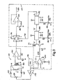
- Figures 2-6 are electrical schematics of circuitry for analyzing signals from the probe and for producing control signals used in generating the images of the workpiece shape;
- Figures 7A-7C are representative images of a workpiece cross-section as depicted on an image screen; and
- Figures 8A-8C illustrate probe output waveforms for generating the Figure 7A-7C images.
- Turning now to the drawings, and in particular Figure 1, an
elongated metal workpiece 10 is driven in a direction indicated by anarrow 12 past a test head supporting two differentially wound energization and detection coils 14, 16. Apparatus for moving the workpiece past the detection coils 14, 16 is disclosed in the referenced and incorporated application to Harris et al. - A
stainless steel sleeve 20 is rotatably supported about the workpiece path of travel so that two slots orapertures 22 in the sleeve rotate beneath the differentially wound coils. The coils are energized with the high frequency signal which sets up magnetic fields in the vicinity of theworkpiece 10. Thesleeve 20 is rotated about the workpiece as the detection coils are energized so that the apertures orslots 22 periodically disrupt this magnetic field at different locations about theworkpiece 10. - The
coils coil 14 and a negative spike from theoppositely wound coil 16. The apertures orslots 22 are angularly offset with respect to each other so that first a positive and then a negative signal is generated by a flaw on the workpiece surface. Analyzing circuitry 110 (Figure 4) coupled to thedlfferentially wound coil 14 creates signals suitable for real time imaging of a cross-section of the workpiece. - The illustration in Figure 7A shows the flaw indicating capability of the present invention. In that Figure the shape of the workpiece is viewed on an
oscilloscope 23. The shape is acceptable, i.e. forms auniform circle 10c in cross-section but adeep flaw 15d exists at the workpiece surface at an orientation of approximately 120° from the vertical. - Turning now to Figure 7B, a different analyzing capability of the invention is displayed on the
oscilloscope 23. It is seen that a cross-section of theworkpiece 10 approximates a circle. Theworkpiece 10, however, is mis-centered within thesleeve 20. This would indicate a defect or mis-adjustment in apparatus for moving the workpiece past the coils and suggest maintenance and/or modification of the apparatus to center the workpiece is in order. - The Figure 7C illustration shows a hexagonal shaped
bar 10 centered within thesleeve 20. If the shape of the bar were non-uniform with excessively rounded corners, for example, this would be apparent. Also, if the bar is to be circular yet appears to be rectangular with rounded corners this defect will be apparent and corrective measures can be taken. - Viewing these representations, the operator of the apparatus can readily ascertain the existence of a flaw and a non-uniform or a non-centered workpiece without examining hard to interpret signal variations on an oscilloscope sweep.
- The Figure 7A-7C representations are created with the aid of the circuitry 110 (Figure 4) which generates X and Y deflection inputs to an
oscilloscope 23. Thecircuitry 110 generates one signal representing a distance between onecoil 16 and the workpiece surface as the slottedsleeve 20 rotates about the workpiece and generates a second signal representing flaw location and depth. The two signals are time multiplexed and scaled by a factor indicating the instantaneous orientation of the sleeve with respect to the workpiece. - Figure 4 presents an overview of the analyzing
circuitry 110. Two outputs 111a, b from the detection coils 14, 16 are coupled to first andsecond demodulator circuits demodulator Circuit 112 is flat when no flaw exists on the workpiece surface and is a pulse or spike when a seam or flaw is detected. The height of the pulse represents flaw depth. - A distance between the
coil 16 and the workpiece surface is represented by the output from thesecond demodulator circuit 114. The magnitude of this signal is related to a distance between thecoil 16 and workpiece surface at the circumferential position of theaperture 22 beneath thecoil 16. A flat response from thedemodulator 114 indicates a uniform circular cross-section bar centered within the sleeve. - A summing and shaping
circuit 116 halfwave rectifies the signal from thedemodulator circuit 112 after those signals pass through 1 kilohertz bandpass filter 115. The rectified output is combined with a D.C. signal from a voltage source 117 proportional to an outside diameter of the workpiece. In an analogous manner the signal from thedemodulator 114 is level shifted with a D.C. bias from asecond voltage source 119. Subsequent to this D.C. level shift the two outputs are coupled to amultiplex unit 118 which alternates first a flaw indicative signal and then a workpiece shape indicative signal. The multiplexed signals are each coupled to twoanalog multiplier circuits oscilloscope 23. - Synchronization and timing is provided to the X and Y deflection controls by a
pulse shaper 130 coupled to a detection coil 132 (Figure 1) which monitors rotation of amagnetic device 134 connected to therotating sleeve 20. Thispulse shaper circuit 130 receives spike inputs from thedetector coil 132 and shapes those spikes into a square wave pulse. Amultiplier circuit 140 is synchronized by an output from thepulse shaper 130 and generates 128 equally spaced pulses between receipt of each pulse shaper signal. An output fromfrequency multiplier 140 is used as a clock input to twophase shifter circuits phase shift circuit 142 which in turn triggers an output to a synchronizedsine wave generator 150 which provides a scaling input to thefirst analog multiplier 120. A delay applied by the first phase shifter can be programmed to be between 0 and 64 clock pulses as defined by thefrequency multiplier 140. This delay allows the location of a flaw to be accurately depicted on an image screen. Thesecond phase shifter 144 generatespulses 90° of sleeve rotation out of phase with respect to thefirst phase shifter 142. This delay or phase shift synchronizes a second sine wave generator 152. - On alternate revolutions of the shield, first the shape and then the flaw signal is transmitted by the
multiplexer 118. The timing of this transmission is controlled by abi-stable flip flop 154 clocked by the output from thepulse shaper 130. If the sleeve rotation is 100 hertz then the shape and flaw signals are each presented by themultiplexer 118 fifty times per second. - Scaling these real time signals with a sine function at the
first analog multiplier 120 results in a continuous output 124 of the form (F)(sin ϑ) and (S) (sin ϑ) where F is the flaw signal and S the shape signal. This scaled signal is coupled to Y axis deflection control to an oscilloscope and represents the instantaneous Y component of the workpiece diameter if the shape signal is being displayed or the Y axis component of a flaw depicting signal if the flaw signal is displayed. At a rate of 50 hertz the human eye perceives both displays so that both flaw and shape signals appear on the screen. The 90 degree phase shift by thephase shifter 144 triggers the second sinewave generator 152 to produce an input to themultiplier 122 which is scaled with the output from themultiplexer 118 to produce an output 126 of the the form (F) (cos ϑ) and (S)(cos ϑ). This signal serves as the X deflection oscilloscope control. The result of this scaling and deflection control by themultipliers - The
phase shift circuit 142 allows the image to be adjusted empirically until the orientation of flaws in a test workpiece are properly oriented on the display. By suitably delaying the scaling signals the flaw orientation is rotated around the image. - An energization and
detection circuit 155 for thecoils kilohertz oscillator 156 drives thecoils resistor 158 and twovariable capacitors coils operational amplifier 164 through atransformer 166. An output from theoperational amplifier 164 is coupled to thefirst demodulator 112. Asecond transformer 170 andoperational amplifier 172 couple the signal across onecoil 16 to thesecond demodulator 114. - Referring to Figure 3, a portion of the
interface 155 is shown coupled to thedemodulator 112. Theoscillator 156 drives apower amplifier 174 which in turn is coupled to the two differentially wound coils 14, 16. Interposed between thepower amplifier 174 and coils are thevariable resistor 158 and two tuning and phase shiftingvariable capacitors coils - When these eddy currents are disrupted by the presence of a flaw, the self induced current through the coils is also disrupted. The interaction of the fields with the sleeve and a workpiece flaw results in a spike or a pulse output from the
coils transformer 166. The output from a secondary of thetransformer 166 is coupled to theamplifier 164 which has an output coupled to an analog switch 176 in thedemodulator circuit 112. The analog switch 176 has agate input 178 which selectively transmits signals through the switch 176 to acapacitor 180 andbuffer amplifier 182. Anoutput 183 from thisbuffer 182 is transmitted to the filter circuit 115. - A gate signal for the analog switch originates at the
oscillator 156. The gate signal is a pulse which periodically couples the analog gate input to its output. An output from theoscillator 156 is coupled to acomparator 184 which transmits a positive portion of the alternating current signal from theoscillator 156 to a switchingtransistor 186 for converting the analog output from theoscillator 156 into a series of pulses. A first one shot 188 produces a delay in these pulses of from 7 to 16 microseconds depending on the setting of avariable 20k resistor 190. A second one shot 192 varies the width of its output pulse from one to five microseconds depending on the setting of a10k variable resistor 194. - A 40 kilohertz oscillator output produces a time or period between peak-to-peak signals of 25 microseconds. The ability to shift and shape the gating signal within this 25 microsecond period allows the user to maximize the output and sensitivity of the flaw detection. The signal from the
amplifier 182 is a voltage output whose magnitude varies with the presence of a flaw. - The filter circuit 115 comprises four integrated circuits, each having four operational amplifiers for a total of sixteen operational amplifiers. The filter circuit is divided into a high pass filter and a low pass filter with the first eight operational amplifiers making up the high pass filter and the next eight operational amplifiers making up the low pass filter. In a preferred embodiment of the invention, these filters in combination attenuate all signals having frequencies less than or greater than approximately one kilohertz. In this way extraneous signals in the noisy environment of a steel production facility are eliminated and only signals generated by flaws in the workpiece will be transmitted to the summing and shaping
circuit 116. - Figure 5 shows in greater detail a major portion of the circuitry of Figure 4. Two
inputs demodulator circuits operational amplifier 216. Theoperational amplifier 216 is configured as a precision rectifier so that negative portions of the Figure 8A signal are eliminated. An optional diode 217 coupled to the output of theprecision rectifier 216 performs a thresholding function to eliminate small positive signals from this output. The end result is a single positive pulse having a height related to the depth of the flaw. The size of this pulse is adjusted with aflaw gain potentiometer 218 having an output coupled to the inverting input of aoperational amplifier 220. - The
amplifier 220 operates as a summing amplifier. A D.C. level shift is added by the voltage source 117 which is preferably avariable potentiometer 222, to the non-inverting input of theoperational amplifier 220. Theoutput 224 from this amplifier is a signal of constant magnitude unless a pulse generated by a flaw at the workpiece surface is encountered at which point the magnitude of the ouput is decreased by an amount proportional to the flaw depth. Therefore oneinput 224 to themultiplex unit 118 is a time varying signal having an information content depicting both location and severity of a flaw in theworkpiece 10. - The
second input 212 contains shape information which is coupled through acoupling capacitor 230 to ashape gain potentiometer 232. This signal is also a time varying signal having a magnitude related to a distance between thecoil 16 and a workpiece surface directly beneath theaperture 22 in thesleeve 20. If a uniform cross-section bar of a circular shape is off center as it passes through the rotating sleeve, a time varying signal (Figure 8B) will be generated since the instantaneous distance between the workpiece surface and the coil in the vicinity of the aperture or slot varies with time. This signal is input to a non-inverting input of anoperational amplifier 234 having a second input coupled to thevoltage source 119 which is preferably avariable potentiometer 236. The input from this potentiometer is adjustable and can be adjusted to provide a suitable off-set to the shape signal. An output 238 from theoperational amplifier 234 is therefore a time varying signal having an instantaneous value related to the distance between the workpiece surface and thecoil 16 at the vicinity of the rotating slot in the sleeve. The output from themultiplexer 118 is coupled to the two scalingmultiplier units MPY 100. - The two trigger signals from the
pulse shaper 30 andfrequency multiplier 140 are seen as twoinputs multiplier circuits rotation phase shifter 142 is set by the user by adjusting the setting on a set of sixswitches 254 coupled to the phase shifter. A pulse from the first trigger is delayed by anywhere from 1 to 64 clock signals generated by thesecond trigger input 252. Since thefrequency multiplier 140 divides the interval betweentrigger # 1 pulses into 128 equally spaced pulses, a time delay of between 1 and 64 clock signals results in delay of transmission of the first trigger pulse of up to one half of a sleeve rotation. This trigger signal is then transmitted directly to a first phaselock loop circuit 256. - Inserted between a second phase
lock loop circuit 258 and the first trigger signal is adelay circuit 260 which in a preferred embodiment delays transmittal of the first trigger signal by 30 clock signals defined by thesecond trigger input 252. This 30 clock signal delay has been empirically determined to be an appropriate delay to produce a 90 degree phase shift between inputs to the two phaselock loop circuits lock loop circuits 256 is illustrated in Figure 6. It is to be appreciated that a second phase lock loop circuit is identical to this circuit in all respects. - Turning now to Figure 6, the phase
lock loop circuit 256 includes afrequency comparator 270 having twoinputs first input 272 is coupled to the trigger signal through a squaringtransistor 276. Internal to thefrequency comparator 270 is a mechanism for storing the time interval between receipt of signals at theinput outputs 275a, b which varies with the frequency of theinput 272. The larger the frequency of the signals appearing at thisinput 272 the larger the voltage output. - A second portion of the phase lock loop circuit shown in Figure 6 is a
sine wave generator 278 which generates a constant amplitude sine wave signal whose frequency is determined by the voltage at aninput 280. The Figure 6 circuitry, thus, receives a series of pulse inputs and converts the pulses into asinusoidal waveform output 282 in the form of a sine wave having a frequency equal to the frequency of the signal appearing at theinput 272. Acomparator circuit 284 generates theinput 274 to thephase comparator 270. This comparison insures that the frequency of the sine wave generator tracks the frequency of the incoming signals 272. Changes in the input frequency result in a discrepancy between the signals at the twoinputs - Returning now to Figure 5, an output from the phase
lock loop circuits inverter circuit 290 depending on the setting of aswitch 292. This switch inverts the phase lock loop sinusoidal output and may be necessitated by the signal requirements of a particular oscilloscope's input. A level shift is added to this signal and it is then coupled to an associatedmultiplier 120 of 122. The level shift cancels a multiplier offset inherent in theMPY 100 integrated circuit multipliers used in a preferred embodiment. These multipliers are commercially available from the Burr-Brown Co., 6730 S. Tuscon Blvd., Tuscon, Arizona 85706. - Some of the advantages of the invention may be appreciated with reference to Figures 7A-7C and 8A-8C. The waveform in Figure 8A is a plot of voltage versus time at the input 210 (Figure 5). An operator viewing this signal on an oscilloscope or the like may not have an idea of the severity or orientation of the flaw that caused this output. When processed by the Figure 4 circuitry and multiplexed with a shape signal from the amplifier 172 (Figure 2), however, the "X" and "Y" oscilloscope control inputs produce the Figure 7A representation on the
oscilloscope 23. The flaw severity is indicated by the depth of thenotch 15d in thecircle 10a representing the workpiece surface. The orientation of thenotch 15d on the screen gives an indication of the circumferential location of the flaw. This added information is important in analyzing the severity and possible cause of the flaw. - The
shape signal 212 is a constant amplitude signal proportional to the workpiece distance to thecoil 16. In figure 7A the shape signal is used to create anoutline 10a for the workpiece. If the workpiece is off center or out-of-round the waveform, as in 10b indicates this fact to an observer. Note that the flaw information to create thenotch 15d is not visible on theshape signal 212 generated outline since the selective filtering and gain applied to the flaw output 111a is not performed on the shape output 111b. - Figures 8B and 8C show two additional waveforms output from the
amplifier 172 representing shape signals. Again, a user viewing these waveforms would have difficulty confirming the shape of the workpiece. The Figure 4 circuit transforms these waveforms into the oscilloscope images of Figures 7B and 7C. The user can readily determine theimage 10b representing the workpiece surface of Figure 7B is off center and that steps to more properly guide the workpiece should be instituted. In Figure 7C the user sees a Figure 10C representing a well centered hex-shaped bar. A user confronted with the task of interpreting the Figure 8C wave form might not conclude thecoils - In Figures 7A, 7B and 7C the
outline images 17 are generated from flaw signal outputs 111a. When no flaws exist on theworkpiece 10 the flaw signal input to themultiplier 118 is a D.C. signal whose size is adjusted by theD.C. voltage source 119. By adjusting this voltage theshape images circular images 17 to give the user a reference for determining an off-center workpiece travel path. - The disclosed oscilloscope images are presented in essentially real time so that what the viewer sees is what is passing through the sleeve beneath the
coils - Although the present invention has been described with a degree of particularity, it is to be understood that it is the intent that the invention include all modifications and alterations from the disclosed embodiment falling within the scope of the appended claims.
Claims (15)
- Apparatus for testing a metallic workpiece comprising a test coil (14,16) for mounting in proximity to the path of travel of a workpiece (10), means (156) coupled to the test coil for cyclically energising the coil and an electrically conductive sleeve (20) having one or more aperture (22) arranged to modify a magnetic field created by the coil
characterised in that means (110) is coupled to the coil for creating a shape indicating signal related to distance between an outer workpiece surface and the coil as the magnetic field is modified and means (120,122) is coordinated with the field modifying sleeve (20) for scaling the shape indicating, signal to provide an indicating signal suitable for real time imaging of a cross-section of the workpiece and which varies with changes in workpiece shape. - Apparatus according to claim 1 characterised in that a display is coupled to the scaling means (120,122) to depict the indicating signal on a display image screen (23).
- Apparatus according to claim 2 characterised in that means (112) for generating a flaw indicating signal and for displaying said flaw indicating signal on the display image screen (23) is coupled to the scaling means (120,122).
- Apparatus according to claim 3 characterised in that means (118) is provided for time multiplexing said shape and flaw signals, together with scaling means (120,122) for scaling said time multiplexed signals into component signals relative to a reference, whereby said component signals yield a real time image of a workpiece cross-section on the display image screen (23).
- Apparatus according to claim 4 characterised in that means is provided for rotating the field modifying sleeve about the workpiece path to enhance the flaw signals and the scaling means (120,122) includes synchronizing means (130,132,134) for determining the angular orientation of said sleeve (20) and creating a timing signal to coordinate scaling of said signals with rotation of said sleeve.
- Apparatus according to claim 5 characterised in that the scaling means (120,122) multiplies said signals by time varying factors which produce orthogonal components of said signal and said display screen (23) comprises a video monitor with inputs which respond to said orthogonal components to produce a two dimension representation of a workpiece cross-section.
- Apparatus according to claim 1 characterised in that imaging means (23) is coordinated with the field modifying sleeve (20) for displaying an indication of the shape indicating signal as the test coil (14,16) and the field modifying sleeve (20) scan the workpiece (10) to present a real time representation of the workpiece.
- Apparatus according to claim 7 characterised in that further means (112) is coupled to the test coil for generating a flaw signal and time multiplexing means (118) is provided to time multiplex the flaw related signal and the shape indicating signal for displaying on said imaging means (23) an illustration of the flaw about the workpiece (10).
- Apparatus according to claim 1 characterised in that the test coil (14,16) is differentially wound with two portions (14,16) mounted at spaced locations along the workpiece travel path;
the sleeve (20) is rotatably mounted and formed with apertures (22) at said spaced locations for selectively modifying an electromagnetic field created by said coil portions (14,16) to produce a flaw indicating signal across said coil portions;
means (110) is coupled across one of said coil portions (16) for creating a shape indicating signal related to a distance between an outer workpiece surface and said one coil portion (16) in a region of electromagnetic field modification;
means (120,122) is coordinated with the rotation of said sleeve (20) for scaling the shape and flaw signals to provide orthogonal components of said shape and flaw signals, and
display means (23) is provided for displaying said orthogonal components of one or the other or both said flaw signals as said coil and field modifying means scan the workpiece. - Apparatus according to claim 9 characterised in that said means for scal ing comprises a circuit (140,142,144) for monitoring rotation of the sleeve (20) and producing two trigger pulses separated in time by approximately 90 degrees of sleeve rotation; and first and second sine wave generators (150,152) coupled to said trigger pulses to create sine wave scaling signals for scaling said flaw and shape signals.
- Apparatus according to claim 10 characterised in that there is additionally provided a multiplexer circuit (118) for alternately coupling said shape and flaw signals to said scaling means (120,122) so that the display means displays first one and then the other of said orthogonal signal components.
- In eddy current testing, a method for displaying an image of a workpiece comprising the steps of positioning a coil (14,16) next to a workpiece path of movement; energizing said coil with a time varying signal to create an electromagnetic field that induces an eddy current in a workpiece moving along said path, modifying said field at varying locations around the workpiece and monitoring signals in said coil induced by said modified field, characterised by the steps of generating a shape indicating signal related to a distance between the coil and a workpiece surface as the magnetic field is modified,
scaling the shape indicating signal by a factor related to the location about the workpiece of said modified field to provide an indicating signal suitable for real time imaging of a cross-section of the workpiece and to properly orient a visible indication of the shape of the workpiece's outer surface on a screen and displaying said signal on a screen. - A method according to claim 12 characterised in that the modification to the field is accomplished by orbiting a field modifying object (20) about the workpiece and said scaling factor is derived from the instantaneous orientation of said object (20) with respect to said workpiece (10).
- A method according to claim 12 characterised by the step of generating from the monitored signals a further signal relating to the presence of a flaw in the workpiece, time multiplexing the flaw related signal and the distance related signal, scaling these signals by a factor related to the instantaneous location about the workpiece of the modified field and displaying a visible indication of the cross-section of the workpiece using the scaled signals as control signals to position the indication on a display means.
- A method according to claim 14 in which the field is modified by rotating about the workpiece path an electrically conductive sleeve (20) having an aperture (22) characterised by the step of using the motion of the sleeve (20) to coordinate the scaling step with the monitoring step so that the scaling step breaks the flaw related signal and the distance related signal into components along orthogonal directions for use in positioning said visible indication.
Priority Applications (1)
| Application Number | Priority Date | Filing Date | Title |
|---|---|---|---|
| AT86301008T ATE66071T1 (en) | 1985-02-25 | 1986-02-13 | METHOD AND DEVICE FOR INSPECTING A WORKPIECE. |
Applications Claiming Priority (2)
| Application Number | Priority Date | Filing Date | Title |
|---|---|---|---|
| US705149 | 1985-02-25 | ||
| US06/705,149 US4644271A (en) | 1985-02-25 | 1985-02-25 | Method and apparatus for examining a workpiece |
Publications (3)
| Publication Number | Publication Date |
|---|---|
| EP0193315A2 EP0193315A2 (en) | 1986-09-03 |
| EP0193315A3 EP0193315A3 (en) | 1987-08-19 |
| EP0193315B1 true EP0193315B1 (en) | 1991-08-07 |
Family
ID=24832241
Family Applications (1)
| Application Number | Title | Priority Date | Filing Date |
|---|---|---|---|
| EP86301008A Expired - Lifetime EP0193315B1 (en) | 1985-02-25 | 1986-02-13 | Method and apparatus for examining a workpiece |
Country Status (6)
| Country | Link |
|---|---|
| US (1) | US4644271A (en) |
| EP (1) | EP0193315B1 (en) |
| JP (1) | JPH087191B2 (en) |
| AT (1) | ATE66071T1 (en) |
| CA (1) | CA1238685A (en) |
| DE (1) | DE3680687D1 (en) |
Cited By (1)
| Publication number | Priority date | Publication date | Assignee | Title |
|---|---|---|---|---|
| WO2019202435A1 (en) * | 2018-04-16 | 2019-10-24 | Shree Magnets Private Limited | Magnetic apparatus with plurality of pole pieces and search coils for determining shape and/or contour of a work piece |
Families Citing this family (18)
| Publication number | Priority date | Publication date | Assignee | Title |
|---|---|---|---|---|
| US5030911A (en) * | 1980-10-19 | 1991-07-09 | Baker Hughes Incorporated | Method and apparatus for displaying defects in tubular members on a two-dimensional map in a variety of display modes |
| US5019775A (en) * | 1989-07-21 | 1991-05-28 | Iowa State University Research Foundation, Inc. | Calibrating an eddy-current-probe using a modulated thermal energy source |
| US5006800A (en) * | 1989-11-06 | 1991-04-09 | General Electric Company | Eddy current imaging apparatus and method using phase difference detection |
| JP2622536B2 (en) * | 1990-03-16 | 1997-06-18 | 株式会社日本非破壊計測研究所 | Eddy current flaw detection method and device |
| US5066913A (en) * | 1990-05-02 | 1991-11-19 | Westinghouse Electric Corp. | Ferrous metal detector for detecting a broken mandrel in a cold pilgering operation |
| AU673076B2 (en) * | 1993-07-05 | 1996-10-24 | Alan Boyle | A shielded tubular mineral detector |
| US5453688A (en) * | 1993-08-23 | 1995-09-26 | Atomic Energy Of Canada Limited | Rotating probe for inspecting tubes having an eccentric housing for supporting sensing means |
| US5541510A (en) * | 1995-04-06 | 1996-07-30 | Kaman Instrumentation Corporation | Multi-Parameter eddy current measuring system with parameter compensation technical field |
| US6657429B1 (en) | 1995-08-25 | 2003-12-02 | Jentek Sensors, Inc. | Material condition assessment with spatially periodic field sensors |
| US7161350B2 (en) | 1999-09-07 | 2007-01-09 | Jentek Sensors, Inc. | Method for material property monitoring with perforated, surface mounted sensors |
| GB2377028B (en) | 1999-09-20 | 2004-07-28 | Jentek Sensors Inc | Eddy-current sensor arrays |
| US7824244B2 (en) * | 2007-05-30 | 2010-11-02 | Corning Incorporated | Methods and apparatus for polishing a semiconductor wafer |
| US6593737B2 (en) * | 2000-08-24 | 2003-07-15 | Shell Oil Company | Method for measuring the wall thickness of an electrically conductive object |
| US6844722B2 (en) * | 2001-08-09 | 2005-01-18 | Avistar, Inc. | Mutual inductance bridge for detection of degradation in metallic components |
| US6741074B2 (en) | 2002-03-01 | 2004-05-25 | General Electric Company | Method and apparatus for separating electrical runout from mechanical runout |
| DE102012017871A1 (en) * | 2012-09-06 | 2014-03-06 | Institut Dr. Foerster Gmbh & Co. Kg | Differential sensor and method for detecting anomalies in electrically conductive materials |
| JP6362259B2 (en) * | 2014-08-07 | 2018-07-25 | 高島産業株式会社 | Eddy current inspection device |
| WO2024197416A1 (en) * | 2023-03-30 | 2024-10-03 | Evident Canada, Inc. | Eddy current (ec) defect view and defect classification |
Family Cites Families (17)
| Publication number | Priority date | Publication date | Assignee | Title |
|---|---|---|---|---|
| US2938162A (en) * | 1957-01-24 | 1960-05-24 | Roffman Eugene | Non-destructive testing by televisual methods |
| US2998566A (en) * | 1959-03-16 | 1961-08-29 | Russell C Heldenbrand | Apparatus for electro-magnetic inspection |
| US3056081A (en) * | 1959-06-22 | 1962-09-25 | Budd Co | Electromagnetic testing |
| DE1138962B (en) * | 1960-12-27 | 1962-10-31 | Funkwerk Dresden Veb | Device for testing magnetostrictive materials with transverse sound waves |
| US3110860A (en) * | 1961-11-06 | 1963-11-12 | Budd Co | Electromagnetic testing apparatus using an eccentrically mounted annular test coil whose axis is rotated about the workpiece axis |
| US3152302A (en) * | 1962-05-16 | 1964-10-06 | Budd Co | Electromagnetic testing apparatus having a rotating apertured cylinder for spirally scanning cylindrical workpieces |
| US3419797A (en) * | 1966-01-21 | 1968-12-31 | Atomic Energy Commission Usa | Nondestructive eddy current testing device for testing metal tubing and instantaneously displaying the cross section of said tubing |
| JPS5249756B2 (en) * | 1972-10-16 | 1977-12-19 | ||
| US3872379A (en) * | 1973-08-29 | 1975-03-18 | Magnetic Analysis Corp | Eddy current testing apparatus using slotted monoturn conductive members |
| SU565248A1 (en) * | 1974-02-26 | 1977-07-15 | Предприятие П/Я Р-6303 | Modulation vortex-current transducer |
| US4203069A (en) * | 1977-12-29 | 1980-05-13 | Electric Power Research Institute, Inc. | Method and apparatus for non-destructively testing electrically conductive elongate cylindrical components using an eddy current producing coil with a rotor to concentrate the magnetic field in a selected area |
| JPS5940265B2 (en) * | 1978-02-13 | 1984-09-28 | 日本鋼管株式会社 | Thermal billet eddy current flaw detection equipment |
| US4337431A (en) * | 1978-03-13 | 1982-06-29 | United Kingdom Atomic Energy Authority | Eddy current test apparatus for annular welds |
| JPS5550156A (en) * | 1978-10-05 | 1980-04-11 | Sumitomo Metal Ind Ltd | Eddy current loating method and device |
| US4507610A (en) * | 1981-07-30 | 1985-03-26 | Shimadzu Corporation | Apparatus for electromagnetically detecting flaws in metallic objects |
| JPS59218946A (en) * | 1983-05-24 | 1984-12-10 | Nippon Benkan Kogyo Kk | Eddy current flaw detection method and flaw detection detector used in this method |
| US4673879A (en) * | 1984-06-27 | 1987-06-16 | Rupublic Steel Corporation | Eddy current flaw detector having rotatable field defining sleeve for selectively enhancing induced eddy currents in a workpiece |
-
1985
- 1985-02-25 US US06/705,149 patent/US4644271A/en not_active Expired - Fee Related
-
1986
- 1986-01-17 CA CA000499778A patent/CA1238685A/en not_active Expired
- 1986-01-21 JP JP61009072A patent/JPH087191B2/en not_active Expired - Lifetime
- 1986-02-13 DE DE8686301008T patent/DE3680687D1/en not_active Expired - Lifetime
- 1986-02-13 EP EP86301008A patent/EP0193315B1/en not_active Expired - Lifetime
- 1986-02-13 AT AT86301008T patent/ATE66071T1/en active
Cited By (1)
| Publication number | Priority date | Publication date | Assignee | Title |
|---|---|---|---|---|
| WO2019202435A1 (en) * | 2018-04-16 | 2019-10-24 | Shree Magnets Private Limited | Magnetic apparatus with plurality of pole pieces and search coils for determining shape and/or contour of a work piece |
Also Published As
| Publication number | Publication date |
|---|---|
| DE3680687D1 (en) | 1991-09-12 |
| JPH087191B2 (en) | 1996-01-29 |
| ATE66071T1 (en) | 1991-08-15 |
| EP0193315A3 (en) | 1987-08-19 |
| EP0193315A2 (en) | 1986-09-03 |
| JPS61195352A (en) | 1986-08-29 |
| CA1238685A (en) | 1988-06-28 |
| US4644271A (en) | 1987-02-17 |
Similar Documents
| Publication | Publication Date | Title |
|---|---|---|
| US4644271A (en) | Method and apparatus for examining a workpiece | |
| US5485084A (en) | Apparatus and method for detecting structural cracks using a movable detector | |
| EP0107844B1 (en) | Eddy-current defect-detecting system for metal tubes | |
| US4755753A (en) | Eddy current surface mapping system for flaw detection | |
| US4087749A (en) | Method and apparatus for normalizing the outputs of sequentially scanned magnetic flaw detectors | |
| KR100218653B1 (en) | Electromagnetic Induction Tester | |
| US4673879A (en) | Eddy current flaw detector having rotatable field defining sleeve for selectively enhancing induced eddy currents in a workpiece | |
| US5298858A (en) | Method and apparatus for non-destructive testing of electrically conductive materials | |
| US5311128A (en) | Eddy current imaging system using spatial derivatives for flow detection | |
| JPS60152950A (en) | Eddy current nondestructive testing method and device thereof | |
| US6566871B2 (en) | Process and device for testing a workpiece by means of eddy currents | |
| JPH08507144A (en) | Location search for buried conductors | |
| US5473247A (en) | Apparatus for discriminating defects in top and bottom surfaces of objects | |
| JP4903349B2 (en) | Detection of abnormalities in objects made of conductive materials | |
| JPS6314905B2 (en) | ||
| US5334934A (en) | Eddy current probe apparatus and interlaced scanning method for interior inspection of metal devices | |
| US20180217099A1 (en) | Virtual channels for eddy current array probes | |
| US7095410B2 (en) | Method for generating and displaying complex data utilizing color-coded signals | |
| EP1877767A2 (en) | Near fieldtm and combination near fieldtm - remote field electromagnetic testing (et) probes for inspecting ferromagnetic pipes and tubes such as those used in heat exchangers | |
| JPH0599901A (en) | Eddy-current flaw detecting apparatus | |
| SU1429009A1 (en) | Eddy-current self-excited flaw detector | |
| Sengupta | Defect characterisation in Austenitic stainless steel plate weld by multimulti frequency Eddy current testing technique | |
| CN119738469A (en) | Eddy current nondestructive testing method for quantitative penetration of liquid rocket engine injector welds | |
| RU2161795C2 (en) | Method of testing quality of welds of thin-walled metal parts and device for its embodiment | |
| JPH0726938B2 (en) | Eddy current flaw detection method |
Legal Events
| Date | Code | Title | Description |
|---|---|---|---|
| PUAI | Public reference made under article 153(3) epc to a published international application that has entered the european phase |
Free format text: ORIGINAL CODE: 0009012 |
|
| AK | Designated contracting states |
Kind code of ref document: A2 Designated state(s): AT BE CH DE FR GB IT LI LU NL SE |
|
| PUAL | Search report despatched |
Free format text: ORIGINAL CODE: 0009013 |
|
| AK | Designated contracting states |
Kind code of ref document: A3 Designated state(s): AT BE CH DE FR GB IT LI LU NL SE |
|
| 17P | Request for examination filed |
Effective date: 19880218 |
|
| 17Q | First examination report despatched |
Effective date: 19890816 |
|
| GRAA | (expected) grant |
Free format text: ORIGINAL CODE: 0009210 |
|
| AK | Designated contracting states |
Kind code of ref document: B1 Designated state(s): AT BE CH DE FR GB IT LI LU NL SE |
|
| PG25 | Lapsed in a contracting state [announced via postgrant information from national office to epo] |
Ref country code: IT Free format text: LAPSE BECAUSE OF FAILURE TO SUBMIT A TRANSLATION OF THE DESCRIPTION OR TO PAY THE FEE WITHIN THE PRE;WARNING: LAPSES OF ITALIAN PATENTS WITH EFFECTIVE DATE BEFORE 2007 MAY HAVE OCCURRED AT ANY TIME BEFORE 2007. THE CORRECT EFFECTIVE DATE MAY BE DIFFERENT FROM THE ONE RECORDED.SCRIBED TIME-LIMIT Effective date: 19910807 Ref country code: LI Effective date: 19910807 Ref country code: AT Effective date: 19910807 Ref country code: SE Effective date: 19910807 Ref country code: CH Effective date: 19910807 Ref country code: BE Effective date: 19910807 |
|
| REF | Corresponds to: |
Ref document number: 66071 Country of ref document: AT Date of ref document: 19910815 Kind code of ref document: T |
|
| ET | Fr: translation filed | ||
| REF | Corresponds to: |
Ref document number: 3680687 Country of ref document: DE Date of ref document: 19910912 |
|
| REG | Reference to a national code |
Ref country code: CH Ref legal event code: PL |
|
| PG25 | Lapsed in a contracting state [announced via postgrant information from national office to epo] |
Ref country code: LU Free format text: LAPSE BECAUSE OF NON-PAYMENT OF DUE FEES Effective date: 19920229 |
|
| PLBE | No opposition filed within time limit |
Free format text: ORIGINAL CODE: 0009261 |
|
| STAA | Information on the status of an ep patent application or granted ep patent |
Free format text: STATUS: NO OPPOSITION FILED WITHIN TIME LIMIT |
|
| 26N | No opposition filed | ||
| PGFP | Annual fee paid to national office [announced via postgrant information from national office to epo] |
Ref country code: DE Payment date: 19960112 Year of fee payment: 11 |
|
| PGFP | Annual fee paid to national office [announced via postgrant information from national office to epo] |
Ref country code: GB Payment date: 19960115 Year of fee payment: 11 |
|
| PGFP | Annual fee paid to national office [announced via postgrant information from national office to epo] |
Ref country code: FR Payment date: 19960116 Year of fee payment: 11 |
|
| PGFP | Annual fee paid to national office [announced via postgrant information from national office to epo] |
Ref country code: NL Payment date: 19960123 Year of fee payment: 11 |
|
| PG25 | Lapsed in a contracting state [announced via postgrant information from national office to epo] |
Ref country code: GB Effective date: 19970213 |
|
| PG25 | Lapsed in a contracting state [announced via postgrant information from national office to epo] |
Ref country code: NL Effective date: 19970901 |
|
| GBPC | Gb: european patent ceased through non-payment of renewal fee |
Effective date: 19970213 |
|
| PG25 | Lapsed in a contracting state [announced via postgrant information from national office to epo] |
Ref country code: FR Effective date: 19971030 |
|
| PG25 | Lapsed in a contracting state [announced via postgrant information from national office to epo] |
Ref country code: DE Effective date: 19971101 |
|
| NLV4 | Nl: lapsed or anulled due to non-payment of the annual fee |
Effective date: 19970901 |
|
| REG | Reference to a national code |
Ref country code: FR Ref legal event code: ST |