EP0192511A1 - Method of producing a diode having a self-aligned contact plug with a gate - Google Patents
Method of producing a diode having a self-aligned contact plug with a gate Download PDFInfo
- Publication number
- EP0192511A1 EP0192511A1 EP86400105A EP86400105A EP0192511A1 EP 0192511 A1 EP0192511 A1 EP 0192511A1 EP 86400105 A EP86400105 A EP 86400105A EP 86400105 A EP86400105 A EP 86400105A EP 0192511 A1 EP0192511 A1 EP 0192511A1
- Authority
- EP
- European Patent Office
- Prior art keywords
- layer
- diode
- substrate
- polycrystalline silicon
- grid
- Prior art date
- Legal status (The legal status is an assumption and is not a legal conclusion. Google has not performed a legal analysis and makes no representation as to the accuracy of the status listed.)
- Granted
Links
- 238000000034 method Methods 0.000 title claims abstract description 45
- 239000000758 substrate Substances 0.000 claims abstract description 23
- 229910021420 polycrystalline silicon Inorganic materials 0.000 claims abstract description 18
- 238000000151 deposition Methods 0.000 claims abstract description 10
- 239000004065 semiconductor Substances 0.000 claims abstract description 6
- 239000003989 dielectric material Substances 0.000 claims abstract description 5
- VYPSYNLAJGMNEJ-UHFFFAOYSA-N Silicium dioxide Chemical compound O=[Si]=O VYPSYNLAJGMNEJ-UHFFFAOYSA-N 0.000 claims description 25
- HQVNEWCFYHHQES-UHFFFAOYSA-N silicon nitride Chemical compound N12[Si]34N5[Si]62N3[Si]51N64 HQVNEWCFYHHQES-UHFFFAOYSA-N 0.000 claims description 15
- 229910052581 Si3N4 Inorganic materials 0.000 claims description 14
- 239000000377 silicon dioxide Substances 0.000 claims description 11
- 238000005468 ion implantation Methods 0.000 claims description 5
- 238000004519 manufacturing process Methods 0.000 claims description 5
- 239000012535 impurity Substances 0.000 claims description 4
- 239000011159 matrix material Substances 0.000 claims description 4
- 238000009792 diffusion process Methods 0.000 claims description 3
- 150000002500 ions Chemical class 0.000 claims 1
- XUIMIQQOPSSXEZ-UHFFFAOYSA-N Silicon Chemical compound [Si] XUIMIQQOPSSXEZ-UHFFFAOYSA-N 0.000 description 23
- 229910052710 silicon Inorganic materials 0.000 description 23
- 239000010703 silicon Substances 0.000 description 23
- 238000003860 storage Methods 0.000 description 6
- 239000000945 filler Substances 0.000 description 5
- 230000015572 biosynthetic process Effects 0.000 description 3
- 238000005530 etching Methods 0.000 description 3
- 238000002513 implantation Methods 0.000 description 3
- 238000000206 photolithography Methods 0.000 description 3
- 238000001465 metallisation Methods 0.000 description 2
- 230000003647 oxidation Effects 0.000 description 2
- 238000007254 oxidation reaction Methods 0.000 description 2
- 229910052814 silicon oxide Inorganic materials 0.000 description 2
- 229910052782 aluminium Inorganic materials 0.000 description 1
- XAGFODPZIPBFFR-UHFFFAOYSA-N aluminium Chemical compound [Al] XAGFODPZIPBFFR-UHFFFAOYSA-N 0.000 description 1
- 238000000637 aluminium metallisation Methods 0.000 description 1
- 239000004020 conductor Substances 0.000 description 1
- 238000010276 construction Methods 0.000 description 1
- 230000003247 decreasing effect Effects 0.000 description 1
- 238000010586 diagram Methods 0.000 description 1
- 239000011810 insulating material Substances 0.000 description 1
- 238000009413 insulation Methods 0.000 description 1
- 239000012212 insulator Substances 0.000 description 1
- 230000000873 masking effect Effects 0.000 description 1
- 229910044991 metal oxide Inorganic materials 0.000 description 1
- 150000004706 metal oxides Chemical class 0.000 description 1
- 150000004767 nitrides Chemical class 0.000 description 1
- 230000035945 sensitivity Effects 0.000 description 1
Images


Classifications
-
- H—ELECTRICITY
- H01—ELECTRIC ELEMENTS
- H01L—SEMICONDUCTOR DEVICES NOT COVERED BY CLASS H10
- H01L21/00—Processes or apparatus adapted for the manufacture or treatment of semiconductor or solid state devices or of parts thereof
- H01L21/02—Manufacture or treatment of semiconductor devices or of parts thereof
- H01L21/027—Making masks on semiconductor bodies for further photolithographic processing not provided for in group H01L21/18 or H01L21/34
- H01L21/033—Making masks on semiconductor bodies for further photolithographic processing not provided for in group H01L21/18 or H01L21/34 comprising inorganic layers
-
- H—ELECTRICITY
- H01—ELECTRIC ELEMENTS
- H01L—SEMICONDUCTOR DEVICES NOT COVERED BY CLASS H10
- H01L21/00—Processes or apparatus adapted for the manufacture or treatment of semiconductor or solid state devices or of parts thereof
- H01L21/02—Manufacture or treatment of semiconductor devices or of parts thereof
- H01L21/04—Manufacture or treatment of semiconductor devices or of parts thereof the devices having potential barriers, e.g. a PN junction, depletion layer or carrier concentration layer
- H01L21/18—Manufacture or treatment of semiconductor devices or of parts thereof the devices having potential barriers, e.g. a PN junction, depletion layer or carrier concentration layer the devices having semiconductor bodies comprising elements of Group IV of the Periodic Table or AIIIBV compounds with or without impurities, e.g. doping materials
- H01L21/30—Treatment of semiconductor bodies using processes or apparatus not provided for in groups H01L21/20 - H01L21/26
- H01L21/31—Treatment of semiconductor bodies using processes or apparatus not provided for in groups H01L21/20 - H01L21/26 to form insulating layers thereon, e.g. for masking or by using photolithographic techniques; After treatment of these layers; Selection of materials for these layers
- H01L21/3205—Deposition of non-insulating-, e.g. conductive- or resistive-, layers on insulating layers; After-treatment of these layers
- H01L21/321—After treatment
-
- H—ELECTRICITY
- H01—ELECTRIC ELEMENTS
- H01L—SEMICONDUCTOR DEVICES NOT COVERED BY CLASS H10
- H01L21/00—Processes or apparatus adapted for the manufacture or treatment of semiconductor or solid state devices or of parts thereof
- H01L21/70—Manufacture or treatment of devices consisting of a plurality of solid state components formed in or on a common substrate or of parts thereof; Manufacture of integrated circuit devices or of parts thereof
- H01L21/71—Manufacture of specific parts of devices defined in group H01L21/70
- H01L21/768—Applying interconnections to be used for carrying current between separate components within a device comprising conductors and dielectrics
- H01L21/76838—Applying interconnections to be used for carrying current between separate components within a device comprising conductors and dielectrics characterised by the formation and the after-treatment of the conductors
- H01L21/76886—Modifying permanently or temporarily the pattern or the conductivity of conductive members, e.g. formation of alloys, reduction of contact resistances
- H01L21/76888—By rendering at least a portion of the conductor non conductive, e.g. oxidation
-
- H—ELECTRICITY
- H01—ELECTRIC ELEMENTS
- H01L—SEMICONDUCTOR DEVICES NOT COVERED BY CLASS H10
- H01L27/00—Devices consisting of a plurality of semiconductor or other solid-state components formed in or on a common substrate
- H01L27/14—Devices consisting of a plurality of semiconductor or other solid-state components formed in or on a common substrate including semiconductor components sensitive to infrared radiation, light, electromagnetic radiation of shorter wavelength or corpuscular radiation and specially adapted either for the conversion of the energy of such radiation into electrical energy or for the control of electrical energy by such radiation
- H01L27/144—Devices controlled by radiation
- H01L27/146—Imager structures
- H01L27/148—Charge coupled imagers
- H01L27/14831—Area CCD imagers
-
- Y—GENERAL TAGGING OF NEW TECHNOLOGICAL DEVELOPMENTS; GENERAL TAGGING OF CROSS-SECTIONAL TECHNOLOGIES SPANNING OVER SEVERAL SECTIONS OF THE IPC; TECHNICAL SUBJECTS COVERED BY FORMER USPC CROSS-REFERENCE ART COLLECTIONS [XRACs] AND DIGESTS
- Y10—TECHNICAL SUBJECTS COVERED BY FORMER USPC
- Y10S—TECHNICAL SUBJECTS COVERED BY FORMER USPC CROSS-REFERENCE ART COLLECTIONS [XRACs] AND DIGESTS
- Y10S148/00—Metal treatment
- Y10S148/082—Ion implantation FETs/COMs
Definitions
- the present invention relates to a method for obtaining a diode whose contact point is self-aligned with a grid.
- the invention applies in particular to the making of contact points at the junctions of drains or sources of the unipolar transistors known under the designation MOS which is the abbreviation of "Metal Oxide Semiconductor" and to those of the photosensitive elements of the matrices line transfer.
- MOS Metal Oxide Semiconductor
- the diode is self-positioned with respect to the grid, but the contact must be made after the oxidation which follows the implantation of diffusion of the impurities which form the junction of the diode, therefore it is not no longer possible to precisely position the contact area with respect to the grid, there is therefore a risk of short circuit between the diode and the grid, by means of metallization.
- the object of the invention is to overcome the aforementioned drawbacks.
- the subject of the invention is a process for obtaining a diode, the contact point of which is self-aligned with a grid, characterized in that it consists in depositing on a semiconductor substrate at least a first layer of dielectric material, to deposit on the last dielectric layer a layer of polycrystalline silicon to form the grid and then a second layer of polycrystalline silicon above the first layer, to be etched in the polycrystalline silicon layers from the contact diode until the dielectric layer is exposed, to oxidize the second layer of polycrystalline silicon sufficiently so that the oxidized layer completely covers the first layer of silicon forming the grid and only covers partially the exposed part of the dielectric layer and to doping the part of the substrate not covered by the oxide layer to form the junction of the diode.
- the method according to the invention has the main advantage that it makes it possible to make an interconnection contact with a diode, of the same dimensions as the latter and self-aligned with respect to a grid by the fact that the diode, the contact and part of the grid are made with the same level of masking.
- the method according to the invention also has the advantage of eliminating a photolithography which makes it possible to improve the compactness of the products produced. It also makes it possible to reduce the depth of the diode junction, which can be formed just before the aluminum metallization of the contact points.
- the method according to the invention eliminates the risks of short-circuiting the grids with the adjacent elements.
- FIGS. 1A, 1B and 1C represent the phases of obtaining a contact diode according to a photolithography process.
- a photo-grid is first produced in the manner shown in FIG. 1A by depositing on a semiconductor substrate 1 a first layer of silica 2, then a second layer of silicon nitride 3 above of the silica layer 2, and finally to form a grid by photolitography on a conductive silicon layer 4.
- the photo-diode is then formed, as shown in FIG. 1B, by ion implantation in a zone 6 of the substrate 1, self-aligned with the grid 4 through a mask 5.
- the photo-contact is then formed in the step shown in FIG.
- the method according to the invention which is described below using FIGS. 2A to 2D, overcomes this drawback. It consists, in a first step shown in FIG. 2A, of depositing on a silicon substrate 9 a first layer 10 of silica then a second layer of silicon nitride 11 above the first layer of silica 10 and then to form by photolithography on a first deposit of polycrystalline silicon 12 the grid to be produced, then to cover the first layer of silicon 12 with a second layer of polycrystalline silicon 13.
- the layers of polycrystalline silicon 12 and 13 are etched to expose the layer of silicon nitride 11 inside a window 14 formed at the place where the diode is to be formed. Then, at the step shown in FIG.
- the silicon layer 13 is oxidized to isolate the grid formed by the polycrystalline silicon layer 12.
- the layer of silicon nitride 1 and the layer of silica 10 are attacked to expose the upper face of the substrate in the window 14 formed by the previous etching, and the diode is formed inside the window 14 by ion implantation or by diffusion of impurities in the substrate 9 inside the window 14 which has the advantage of making it possible to practice a minimum drawing time of the implanted or diffused impurities and makes it possible to obtain a lower junction depth.
- the diode may be formed with the step shown in FIG.
- the method according to the invention makes it possible to obtain an interconnection contact of the diode of the same dimensions as the diode itself, which improves the compactness of the products obtained and makes it possible in the first case to decrease the junction depth of the diode which can be formed just before the metallization operation, by aluminum, for example, contact points.
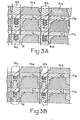
- FIG. 3A represents a line transfer matrix having diodes with contact points obtained according to the method of the known art described previously using FIGS. 1A and 1B.
- the matrix shown consists of four parts, a first part is formed by a set of storage diodes 15a to 15f representing photosensitive surface elements, a second part is formed by a set of readout diodes 16a to 16d, a third part is formed by grids 17a to 17b to control the passage of electric charges between the storage diodes and the reading diodes, and a fourth part is formed by the interconnection lines 18a 18b connected to the reading diodes for transferring, for example, loads read to an outdoor CCD reader.
- the interconnection lines are perpendicular to the control grids for the passage of charges and a thick oxide 19 isolates the photosensitive surfaces 15a to 15f from the read diodes 16a to 16d.
- the method according to the invention makes it possible to exercise control over the dimensions of the contact opening as a function of the thickness of the silicon layer 13 used.
- the contact dimension n which is obtained depends, on the one hand, on the nominal dimension m of the window made in the silicon layer 12 and on the other hand, of the thickness of the oxide formed 13.
- the greater the thickness of the oxide formed 18 the more the dimensions of the contact opening of the diodes 16a to 16d decrease and the more it is possible to increase the photosensitive surface of the storage diodes 15a to 15f. This result goes against the results obtained by traditional methods, because returning to FIG.
- the contact opening in a usual process consists in attacking the insulating layer of silicon oxide 7 through a mask M which results in obtaining an opening n shown in FIG. 5 which can only increase as a function of the thickness of the oxide layer 7 produced relative to the opening m made in the mask M.
- MOS transistor source drain contact points can be obtained using the method according to the invention, either by forming the contact diodes of the MOS transistor at the end of the process for obtaining the transistor, or by forming the diodes. before the second silicon deposit.
- the procedure is as in FIG. 2A by depositing on a semiconductor substrate 20 a first layer of silica 21 followed by a second layer of silicon nitride 22 and depositing above the layer of silicon nitride 22 a first layer of silicon 23, then a second layer of silicon 24, the latter then being transformed into oxide to form the insulator of the grid.
- the silicon layers 23 and 24 are etched as shown in FIG.
- the gate G of the transistor and two windows 25 and 26 located on either side of the gate G.
- the layer of silicon nitride 22 and the thin layer of silicon oxide 21 are removed to allow access to the substrate 20 for ion implantation of the substrate 20 through windows 25 and 26.
- the diodes are formed before the formation of the gate-connection insulating oxide. Self-alignment is then possible by protecting the silicon nitride by an excess in the grid of the future contact zone.
- the silicon layer 23 forming the grid is first of all covered with a layer of filler silicon 24 (FIG. 7B) then the filler silicon and the layer of silicon forming the grid are etched to form the window 25 ( FIG. 7C) and reveal the layer of silicon nitride 22 (FIG. 7D) so as not to have discontinuities between the diode and the contact zone which will subsequently be doped (FIG. 7E).
- the method according to the invention is also applicable to the manufacture of diodes produced while keeping the nitride-oxide double layer, according to the stages of the method represented in FIGS. 8A to 8E.
- this method after implantation (FIG. 8A) of the diode through the double layer of silica 21 and of silicon nitride 22, the filler silicon 24 is deposited above the silicon layer 23 (FIG. 8B), then the filler silicon is etched in the manner shown in FIG.
- the self-alignment can then be carried out by etching the silicon of the grid at the same time as the layer of filler silicon and after the phase of oxidation shown in Figure 8D, the junction is accessed by attacking the silicon nitride layer 22 and the thin oxide layer 21.
Landscapes
- Engineering & Computer Science (AREA)
- Power Engineering (AREA)
- Physics & Mathematics (AREA)
- Condensed Matter Physics & Semiconductors (AREA)
- General Physics & Mathematics (AREA)
- Computer Hardware Design (AREA)
- Microelectronics & Electronic Packaging (AREA)
- Manufacturing & Machinery (AREA)
- Inorganic Chemistry (AREA)
- Chemical & Material Sciences (AREA)
- Electromagnetism (AREA)
- Solid State Image Pick-Up Elements (AREA)
- Electrodes Of Semiconductors (AREA)
Abstract
Le procédé selon l'invention consiste à déposer sur un substrat semi-conducteur (9) au moins une première couche d'un matériau diélectrique (10, 11), à déposer sur la dernière couche diélectrique (11) une première couche de silicium polycristallin (12) pour former la grille, puis une deuxième couche de silicium polycristallin (13) au-dessus de la première couche (12) à graver dans les couches de silicium polycristallin (12, 13) l'emplacement de la diode contact jusqu'à la mise à nue de la couche diélectrique (10, 11), à oxyder la deuxième couche de silicium polycristallin (13) de manière suffisante pour que la couche oxydée recouvre entièrement la première couche de silicium polycristallin (13) formant la grille et ne recouvre que partiellement la partie mise à nue de la couche diélectrique (10, 11), et à doper la partie du substrat (14) non recouverte par la couche d'oxyde pour former la jonction de la diode. Application: Eléments photosensibles des matrices à transfert de ligne.The method according to the invention consists in depositing on a semiconductor substrate (9) at least a first layer of a dielectric material (10, 11), in depositing on the last dielectric layer (11) a first layer of polycrystalline silicon (12) to form the grid, then a second layer of polycrystalline silicon (13) above the first layer (12) to be etched in the layers of polycrystalline silicon (12, 13) the location of the contact diode up to when the dielectric layer (10, 11) is exposed, the second layer of polycrystalline silicon (13) is oxidized sufficiently so that the oxidized layer completely covers the first layer of polycrystalline silicon (13) forming the grid and does not only partially covers the exposed part of the dielectric layer (10, 11), and to doping the part of the substrate (14) not covered by the oxide layer to form the junction of the diode. Application: Photosensitive elements of line transfer matrices.
Description
La présente invention concerne un procédé d'obtention d'une diode dont la prise de contact est auto-alignée à une grille.The present invention relates to a method for obtaining a diode whose contact point is self-aligned with a grid.
L'invention s'applique notamment à la réalisation des prises de contact au niveau des jonctions de drains ou de sources des transistors unipolaires connus sous la désignation MOS qui est l'abréviation de "Metal Oxyde Semiconducteur" et à celles des éléments photosensibles des matrices de transfert de ligne.The invention applies in particular to the making of contact points at the junctions of drains or sources of the unipolar transistors known under the designation MOS which is the abbreviation of "Metal Oxide Semiconductor" and to those of the photosensitive elements of the matrices line transfer.
Il est connu pour réaliser une diode de faible dimension avec prise de contact adjacente à une ou plusieurs grilles, isolées de la diode par des matériaux isolants, d'opérer selon un procédé photolithographique consistant à créer successivement sur une couche diélectrique recouvrant un substrat semi-conducteur, d'abord une photo-grille puis une photo-diode alignée sur la photo-grille et enfin un photo-contact isolé de la grille. Selon ce procédé la diode est autopositionnée par rapport à la grille, mais la prise de contact doit être effectuée après l'oxydation qui succède à l'implantation de diffusion des impuretés qui forment la jonction de la diode, de ce fait il n'est plus possible de positionner de façon précise la zone de contact par rapport à la grille, il existe donc un risque de court-circuit entre la diode et la grille, par l'intermédiaire de la métallisation.It is known to produce a small diode with contact making adjacent to one or more grids, isolated from the diode by insulating materials, to operate according to a photolithographic process consisting of successively creating on a dielectric layer covering a semi-substrate conductor, first a photo-grid then a photo-diode aligned with the photo-grid and finally a photo-contact isolated from the grid. According to this process the diode is self-positioned with respect to the grid, but the contact must be made after the oxidation which follows the implantation of diffusion of the impurities which form the junction of the diode, therefore it is not no longer possible to precisely position the contact area with respect to the grid, there is therefore a risk of short circuit between the diode and the grid, by means of metallization.
Le but de l'invention est de pallier les inconvénients précités.The object of the invention is to overcome the aforementioned drawbacks.
A cet effet l'invention a pour objet, un procédé d'obtention d'une diode dont la prise de contact est auto-alignée à une grille caractérisé en ce qu'il consiste à déposer sur un substrat semi-conducteur au moins une première couche d'un matériau diélectrique, à déposer sur la dernière couche de diélectrique une couche de silicium polycristallin pour former la grille puis une deuxième couche de silicium polycristallin au-dessus de la première couche, à graver dans les couches de silicium polycristallin l'emplacement de la diode contact jusqu'à la mise à nue de la couche diélectrique, à oxyder la deuxième couche de silicium polycristallin de manière suffisante pour que la couche oxydée recouvre entièrement la première couche de silicium formant la grille et ne recouvre que partiellement la partie mise à nue de la couche diélectrique et à doper la partie du substrat non recouverte par la couche d'oxyde pour former la jonction de la diode.To this end, the subject of the invention is a process for obtaining a diode, the contact point of which is self-aligned with a grid, characterized in that it consists in depositing on a semiconductor substrate at least a first layer of dielectric material, to deposit on the last dielectric layer a layer of polycrystalline silicon to form the grid and then a second layer of polycrystalline silicon above the first layer, to be etched in the polycrystalline silicon layers from the contact diode until the dielectric layer is exposed, to oxidize the second layer of polycrystalline silicon sufficiently so that the oxidized layer completely covers the first layer of silicon forming the grid and only covers partially the exposed part of the dielectric layer and to doping the part of the substrate not covered by the oxide layer to form the junction of the diode.
Le procédé selon l'invention a principalement pour avantage qu'il permet de -réaliser un contact d'interconnexion avec une diode, de mêmes dimensions que celle-ci et auto-aligné par rapport à une grille par le fait que la diode, le contact et une partie de la grille sont réalisés avec le même niveau de masquage. Le procédé selon l'invention a aussi pour avantage de supprimer une photolitographie ce qui permet d'améliorer la compacité des produits réalisés. Il permet également de diminuer la profondeur de la jonction de la diode, celle-ci pouvant être formée juste avant la métalisation aluminium des prises de contact. D'autre part le procédé selon l'invention supprime les risques de mise en court-circuit des grilles avec les éléments limitrophes.The method according to the invention has the main advantage that it makes it possible to make an interconnection contact with a diode, of the same dimensions as the latter and self-aligned with respect to a grid by the fact that the diode, the contact and part of the grid are made with the same level of masking. The method according to the invention also has the advantage of eliminating a photolithography which makes it possible to improve the compactness of the products produced. It also makes it possible to reduce the depth of the diode junction, which can be formed just before the aluminum metallization of the contact points. On the other hand, the method according to the invention eliminates the risks of short-circuiting the grids with the adjacent elements.
D'autres caractéristiques et avantages de l'invention apparaîtront au cours de la description qui suit faite au regard des dessins annexés dans lesquels :
- - les figures lA, 1B et 1C représentent les phases d'un procédé d'obtention d'une diode contact selon l'art connu ;
- - les figures 2A à 2D représentent les phases du procédé d'obtention d'une diode contact selon l'invention ;
- - les figures 3A et 3B représentent deux modes de réalisation d'éléments photosensibles obtenus respectivement à partir du procédé représenté aux figures IA à 1C et du procédé selon l'invention représenté aux figures 2A à 2D ;
- - les figures 4A et 4B représentent une ouverture de contact obtenue en application du procédé selon l'invention ;
- - la figure 5 est une représentation par contraste avec le dessin de la figure 4B d'une ouverture de contact obtenue à l'aide des procédés photolitographiques habituels ;
- - les figures 6A à 6D illustrent un premier mode de réalisation d'un transistor MOS réalisé à l'aide du procédé selon l'invention, les diodes étant formées dans la phase finale du procédé ;
- - les figures 7A à 7E illustrent un deuxième mode de réalisation selon lequel les diodes sont formées avant la formation de l'oxyde d'isolement lié aux connexions ;
- - les figures SA à 8E illustrent un troisième mode de réalisation de diodes contact en conservant la double couche de nitrure-oxyde.
- - Figures lA, 1B and 1C show the phases of a process for obtaining a contact diode according to the known art;
- - Figures 2A to 2D show the phases of the process for obtaining a contact diode according to the invention;
- - Figures 3A and 3B show two embodiments of photosensitive elements obtained respectively from the method shown in Figures IA to 1C and the method according to the invention shown in Figures 2A to 2D;
- - Figures 4A and 4B show a contact opening obtained by applying the method according to the invention;
- - Figure 5 is a representation in contrast with the drawing of Figure 4B of a contact opening obtained using the usual photolitographic methods;
- - Figures 6A to 6D illustrate a first embodiment of a MOS transistor produced using the method according to the invention, the diodes being formed in the final phase of the method;
- - Figures 7A to 7E illustrate a second embodiment according to which the diodes are formed before the formation of the insulation oxide linked to the connections;
- - Figures SA to 8E illustrate a third embodiment of contact diodes while retaining the double layer of nitride-oxide.
Dans le procédé illustré à l'aide des figures lA, 1B et IC qui représentent les phases d'obtention d'une diode contact suivant un procédé de photolitographie de. l'art connu, une photo-grille est d'abord réalisée de la façon représentée à la figure IA en déposant sur un substrat 1 semi- conducteur une première couche de silice 2, puis une deuxième couche de nitrure de silicium 3 au-dessus de la couche de silice 2, et enfin à former une grille par une photolitographie sur une couche de silicium conductrice 4. La photo-diode est formée ensuite, de la manière représentée à la figure IB, par implantation ionique dans une zone 6 du substrat 1, auto-alignée avec la grille 4 au travers d'un masque 5. Le photo-contact est ensuite formé à l'étape représentée à la figure 1C par dépôt d'une couche d'oxyde 7 autour de la couche de silicium 4 formant grille puis par attaque de la couche de nitrure 3 et désoxydation de la couche de silice 2 pour permettre d'accèder au substrat 1 et former l'ouverture de contact 8. En se reportant à la figure 1 C il est apparent que le procédé qui vient d'être décrit ne permet pas de positionner l'ouverture de contact 8 par rapport à la grille 4 avec suffisamment de précision pour éliminer tout risque de court-circuit entre le contact qui sera par la suite formé dans l'ouverture 8 d'accès à la diode 6 et la grille 4.In the process illustrated with the aid of FIGS. 1A, 1B and 1C which represent the phases of obtaining a contact diode according to a photolithography process. prior art, a photo-grid is first produced in the manner shown in FIG. 1A by depositing on a semiconductor substrate 1 a first layer of
Le procédé selon l'invention qui est décrit ci-après à l'aide des figures 2A à 2D, permet de remédier à cet inconvénient. Il consiste, dans une première étape représentée à la figure 2A, à déposer sur un substrat de silicium 9 une première couche 10 de silice puis une deuxième couche de nitrure de silicium 11 au-dessus de la première couche de silice 10 puis à former par photolitogravure sur un premier dépôt de silicium polycristallin 12 la grille à réaliser, puis à recouvrir la première couche de silicium 12 par une deuxième couche de silicium polycristallin 13. A l'étape suivante, représentée à la figure 2B, les couches de silicium polycristallin 12 et 13 sont gravées pour mettre à nue la couche de nitrure de silicium 11 à l'intérieur d'une fenêtre 14 pratiquée à l'endroit où la diode doit être formée. Puis, à Pétape représentée à la figure 2C, la couche de silicium 13 est oxydée pour isoler la grille formée par la couche de silicium polycristallin 12. Enfin, à l'étape représentée à la figure 2D, la couche de nitrure de silicium 1 et la couche de silice 10 sont attaquées pour mettre à nue la face supérieure du substrat dans la fenêtre 14 pratiquée par la gravure précédente, et la diode est formée à l'intérieur de la fenêtre 14 par implantation ionique ou par diffusion d'impuretés dans le substrat 9 à l'intérieur de la fenêtre 14 ce qui a l'avantage de permettre de pratiquer un temps de tirage minimum des impuretés implantées ou diffusées et permet d'obtenir une profondeur de jonction plus faible. On notera, que le mode de réalisation qui vient d'être décrit n'est pas unique et que, selon une variante d'exécution du procédé selon l'invention, la diode pourra être formée à retape représentée à la figure 2C après gravure de la couche de silicium 13 par implantation à travers la double couche de silice 10 et de nitrure de silicium 11. Dans l'une ou l'autre variante de réalisation, le procédé selon l'invention permet d'obtenir un contact d'interconnexion de la diode de mêmes dimensions que la diode elle-même, ce qui améliore la compacité des produits obtenus et rend possible dans le premier cas la diminution de la profondeur de jonction de la diode qui peut être formée juste avant l'opération de métalisation, par l'aluminium, par exemple, des prises de contact. Ces caractéristiques de l'invention permettent de l'appliquer très efficacement à la construction, soit d'éléments photosensibles de matrices à transfert de ligne, soit à la réalisation de prises de contact de sources et de drains de transistors MOS.The method according to the invention which is described below using FIGS. 2A to 2D, overcomes this drawback. It consists, in a first step shown in FIG. 2A, of depositing on a silicon substrate 9 a
Un exemple de réalisation d'éléments photosensibles d'une matrice à transfert de ligne est décrit ci-après à l'aide de schémas représentés aux figures 3A et 3B. La figure 3A représente une matrice à transfert de ligne possédant des diodes avec prises de contacts obtenues suivant le procédé de l'art connu décrit précédemment à l'aide des figures lA et 1B. La matrice représentée se compose de quatre parties, une première partie est formée par un ensemble de diodes de stockage 15a à 15f représentant des éléments de surface photosensible, une deuxième partie est formée par un ensemble de diodes de lecture 16a à 16d, une troisième partie est formée par des grilles 17a à 17b pour commander le passage des charges électriques entre les diodes de stockage et les diodes de lecture, et une quatrième partie est formée par les lignes d'interconnexion 18a 18b reliées aux diodes de lecture pour transférer par exemple, les charges lues vers une barrette CCD de lecture extérieure. Dans cette configuration les lignes d'interconnexion sont perpendiculaires aux grilles de commande du passage des charges et un oxyde épais 19 isole les surfaces photosensibles 15a à 15f des diodes de lecture 16a à 16d.An exemplary embodiment of photosensitive elements of a line transfer matrix is described below using diagrams shown in Figures 3A and 3B. FIG. 3A represents a line transfer matrix having diodes with contact points obtained according to the method of the known art described previously using FIGS. 1A and 1B. The matrix shown consists of four parts, a first part is formed by a set of
Le procédé selon l'invention appliqué à la fabrication des matrices à transfert de ligne, du type de celle qui vient d'être décrite à l'aide de la figure 3A, permet de privilégier les surfaces de stockage pour augmenter la sensibilité de chacun des éléments de stockage 15a à 15f. En diminuant la surface occupée par chacune des diodes de lecture 16a à 16d il devient possible, de la façon représentée à la figure 3B, d'augmenter la surface de chacune des diodes de stockage 15a à 15f en auto-alignant chacune des diodes de lecture 16a à 16d sur leurs grilles de passage respectives 17a et 17b et en contrôlant l'ouverture de contact pratiquée au-dessus de chaque diode 16a à 16d. Contrairement au procédé connu décrit précédemment à l'aide des figures lA à 1C, le procédé selon l'invention permet d'exercer un contrôle des dimensions de l'ouverture de contact en fonction de l'épaisseur de la couche de silicium 13 utilisée. Sur les ouvertures de contact représentées par exemple aux figures 4A et 4B, la cote de contact n qui est obtenue, dépend d'une part, de la cote nominale m de la fenêtre pratiquée dans la couche de silicium 12 et d'autre part, de l'épaisseur de l'oxyde formé 13. En fait, en revenant à la figure 3B, on constate que plus l'épaisseur de l'oxyde formé 18 est importante, plus les dimensions de l'ouverture de contact des diodes 16a à 16d diminuent et plus il est possible d'augmenter la surface photosensible des diodes de stockage 15a à 15f. Ce résultat va à rencontre des résultats obtenus par les procédés traditionnels, car en revenant à la figure 1C l'ouverture de contact dans un processus habituel consiste à attaquer la couche isolante d'oxyde de silicium 7 au travers d'un masque M ce qui a pour résultat l'obtention d'une ouverture n représentée à la figure 5 qui ne peut qu'augmenter en fonction de l'épaisseur de la couche d'oxyde 7 réalisée par rapport à l'ouverture m pratiquée dans le masque M.The method according to the invention applied to the manufacture of line transfer matrices, of the type which has just been described with the aid of FIG. 3A, makes it possible to favor the storage surfaces to increase the sensitivity of each of the
La réalisation de prises de contact source drain de transistor MOS à l'aide du procédé selon l'invention peut être obtenue, soit en formant les diodes contact du transistor MOS à la fin du processus d'obtention du transistor, soit en formant les diodes avant le deuxième dépôt de silicium. Dans le premier cas, représenté aux figures 6A à 6D, on procède comme à la figure 2A par un dépôt sur un substrat semi-conducteur 20 d'une première couche de silice 21 suivie d'une deuxième couche de nitrure de silicium 22 et on dépose au-dessus de la couche de nitrure de silicium 22 une première couche de silicium 23, puis une deuxième couche de silicium 24, cette dernière étant ensuite transformée en oxyde pour former l'isolant de la grille. Les couches de silicium 23 et 24 sont gravées de la façon représentée à la figure 6B pour former, la grille G du transistor et deux fenêtres 25 et 26 situées de part et d'autre de la grille G. Après croissance d'oxyde au-dessus de la couche de silicium 23 de la grille G (figure 6C) la couche de nitrure de silicium 22 et la couche mince d'oxyde de silicium 21 sont retirées pour permettre l'accès au substrat 20 pour procéder à une implantation ionique du substrat 20 au travers des fenêtres 25 et 26.MOS transistor source drain contact points can be obtained using the method according to the invention, either by forming the contact diodes of the MOS transistor at the end of the process for obtaining the transistor, or by forming the diodes. before the second silicon deposit. In the first case, shown in FIGS. 6A to 6D, the procedure is as in FIG. 2A by depositing on a semiconductor substrate 20 a first layer of
Dans le deuxième cas, représenté aux figures 7A à 7E, les diodes sont formées avant la formation de l'oxyde d'isolement grille-connexion. L'auto-alignement est alors possible en protégeant le nitrure de silicium par un excès dans la grille de la future zone de contact. La couche de silicium 23 formant la grille est tout d'abord recouverte d'une couche de silicium d'apport 24 (figure 7B) puis le silicium d'apport et la couche de silicium formant la grille sont gravées pour former la fenêtre 25 (figure 7C) et faire apparaître la couche de nitrure de silicium 22 (figure 7D) pour ne pas avoir de discontinuités entre la diode et la zone de contact qui sera par la suite dopée (figure 7E).In the second case, represented in FIGS. 7A to 7E, the diodes are formed before the formation of the gate-connection insulating oxide. Self-alignment is then possible by protecting the silicon nitride by an excess in the grid of the future contact zone. The
Le procédé selon l'invention est également applicable à la fabrication de diodes réalisées en gardant la double couche nitrure-oxyde, selon les étapes du procédé représenté aux figures 8A à 8E. Selon ce procédé, après implantation (figure 8A) de la diode à travers la double couche de silice 21 et de nitrure de silicium 22, le silicium d'apport 24 est déposé au-dessus de la couche de silicium 23 (figure 8B), puis le silicium d'apport est gravé à la façon représentée à la figure 8C, l'auto-alignement peut alors être réalisé en gravant le silicium de la grille en même temps que la couche de silicium d'apport et après la phase d'oxydation représentée à la figure 8D, la jonction est accédée en attaquant la couche de nitrure de silicium 22 et la couche d'oxyde mince 21.The method according to the invention is also applicable to the manufacture of diodes produced while keeping the nitride-oxide double layer, according to the stages of the method represented in FIGS. 8A to 8E. According to this method, after implantation (FIG. 8A) of the diode through the double layer of
Claims (9)
Applications Claiming Priority (2)
| Application Number | Priority Date | Filing Date | Title |
|---|---|---|---|
| FR8501085 | 1985-01-25 | ||
| FR8501085A FR2576710B1 (en) | 1985-01-25 | 1985-01-25 | METHOD FOR OBTAINING A DIODE WHOSE CONTACT IS SELF-ALIGNED WITH A GRID |
Publications (2)
| Publication Number | Publication Date |
|---|---|
| EP0192511A1 true EP0192511A1 (en) | 1986-08-27 |
| EP0192511B1 EP0192511B1 (en) | 1989-11-08 |
Family
ID=9315629
Family Applications (1)
| Application Number | Title | Priority Date | Filing Date |
|---|---|---|---|
| EP86400105A Expired EP0192511B1 (en) | 1985-01-25 | 1986-01-20 | Method of producing a diode having a self-aligned contact plug with a gate |
Country Status (5)
| Country | Link |
|---|---|
| US (1) | US4692995A (en) |
| EP (1) | EP0192511B1 (en) |
| JP (1) | JPS61176152A (en) |
| DE (1) | DE3666898D1 (en) |
| FR (1) | FR2576710B1 (en) |
Families Citing this family (4)
| Publication number | Priority date | Publication date | Assignee | Title |
|---|---|---|---|---|
| JPH0475964A (en) * | 1990-07-13 | 1992-03-10 | Tokyo Kikai Seisakusho Ltd | Chopper folded paper restricting device for rotary press |
| FR2679379B1 (en) * | 1991-07-16 | 1997-04-25 | Thomson Composants Militaires | METHOD FOR MANUFACTURING INTEGRATED CIRCUITS WITH VERY NARROW ELECTRODES. |
| US6197649B1 (en) * | 1998-08-05 | 2001-03-06 | International Rectifier Corp. | Process for manufacturing planar fast recovery diode using reduced number of masking steps |
| US6445021B1 (en) * | 2000-09-20 | 2002-09-03 | International Business Machines Corporation | Negative differential resistance reoxidized nitride silicon-based photodiode and method |
Citations (3)
| Publication number | Priority date | Publication date | Assignee | Title |
|---|---|---|---|---|
| US4247861A (en) * | 1979-03-09 | 1981-01-27 | Rca Corporation | High performance electrically alterable read-only memory (EAROM) |
| FR2464561A1 (en) * | 1979-08-31 | 1981-03-06 | Thomson Csf | Complementary MOSFET structure handling large voltage - has each transistor enclosed by n-type epitaxial pocket reducing parasitic bipolar transistor gain |
| EP0051534A2 (en) * | 1980-10-29 | 1982-05-12 | FAIRCHILD CAMERA & INSTRUMENT CORPORATION | A method of fabricating a self-aligned integrated circuit structure using differential oxide growth |
Family Cites Families (6)
| Publication number | Priority date | Publication date | Assignee | Title |
|---|---|---|---|---|
| US4477962A (en) * | 1978-05-26 | 1984-10-23 | Rockwell International Corporation | Process for and structure of high density VLSI circuits, having self-aligned gates and contacts for FET devices and conducting lines |
| US4506437A (en) * | 1978-05-26 | 1985-03-26 | Rockwell International Corporation | Process for and structure of high density VLSI circuits, having self-aligned gates and contacts for FET devices and conducting lines |
| US4466172A (en) * | 1979-01-08 | 1984-08-21 | American Microsystems, Inc. | Method for fabricating MOS device with self-aligned contacts |
| FR2461360A1 (en) * | 1979-07-10 | 1981-01-30 | Thomson Csf | METHOD FOR MANUFACTURING A VERTICALLY OPERATING DMOS-TYPE FIELD EFFECT TRANSISTOR AND TRANSISTOR OBTAINED THEREBY |
| US4305200A (en) * | 1979-11-06 | 1981-12-15 | Hewlett-Packard Company | Method of forming self-registering source, drain, and gate contacts for FET transistor structures |
| US4486943A (en) * | 1981-12-16 | 1984-12-11 | Inmos Corporation | Zero drain overlap and self aligned contact method for MOS devices |
-
1985
- 1985-01-25 FR FR8501085A patent/FR2576710B1/en not_active Expired
-
1986
- 1986-01-20 DE DE8686400105T patent/DE3666898D1/en not_active Expired
- 1986-01-20 EP EP86400105A patent/EP0192511B1/en not_active Expired
- 1986-01-22 JP JP61011811A patent/JPS61176152A/en active Pending
- 1986-01-24 US US06/822,028 patent/US4692995A/en not_active Expired - Fee Related
Patent Citations (3)
| Publication number | Priority date | Publication date | Assignee | Title |
|---|---|---|---|---|
| US4247861A (en) * | 1979-03-09 | 1981-01-27 | Rca Corporation | High performance electrically alterable read-only memory (EAROM) |
| FR2464561A1 (en) * | 1979-08-31 | 1981-03-06 | Thomson Csf | Complementary MOSFET structure handling large voltage - has each transistor enclosed by n-type epitaxial pocket reducing parasitic bipolar transistor gain |
| EP0051534A2 (en) * | 1980-10-29 | 1982-05-12 | FAIRCHILD CAMERA & INSTRUMENT CORPORATION | A method of fabricating a self-aligned integrated circuit structure using differential oxide growth |
Non-Patent Citations (3)
| Title |
|---|
| IBM TECHNICAL DISCLOSURE BULLETIN, vol. 22, no. 8B, janvier 1980, pages 3688-3691, New York, US; R.C. VARSHNEY: "Polysilicon oxide process for small line gaps" * |
| IEDM INTERNATIONAL ELECTRON DEVICES MEETING, Washington, DC, 8-10 décembre 1980, Technical Digest, papier 6.3, pages 140-143, IEEE, New York, US; H.S. FU et al.: "A new MOS transistor design with self-registering source-drain and gate contacts" * |
| IEEE ELECTRON DEVICE LETTERS, vol. EDL-3, no. 2, février 1982, pages 40-42, IEEE, New York, US; S. HSIA et al.: "Polysilicon oxidation self-aligned MOS (POSA MOS) - a new self-aligned double source/drain ion implantation technique for VLSI" * |
Also Published As
| Publication number | Publication date |
|---|---|
| FR2576710A1 (en) | 1986-08-01 |
| JPS61176152A (en) | 1986-08-07 |
| FR2576710B1 (en) | 1988-03-04 |
| US4692995A (en) | 1987-09-15 |
| EP0192511B1 (en) | 1989-11-08 |
| DE3666898D1 (en) | 1989-12-14 |
Similar Documents
| Publication | Publication Date | Title |
|---|---|---|
| EP0258141B1 (en) | MIS integrated circuit such as an EPROM memory cell, and method of making the same | |
| US4613402A (en) | Method of making edge-aligned implants and electrodes therefor | |
| US5858843A (en) | Low temperature method of forming gate electrode and gate dielectric | |
| US5747379A (en) | Method of fabricating seamless tungsten plug employing tungsten redeposition and etch back | |
| US5427970A (en) | Method of making flash memory with high coupling ratio | |
| FR2458902A1 (en) | METHOD FOR MANUFACTURING INTEGRATED MOS CIRCUITS WITH AND WITHOUT MNOS MEMORY TRANSISTORS BASED ON SILICON GRID TECHNOLOGY | |
| EP0299853A1 (en) | Process for producing a memory cell | |
| EP0013342B1 (en) | Method of fabrication of self-aligned field-effect transistors of the metal-semiconductor type | |
| US4746622A (en) | Process for preparing a charge coupled device with charge transfer direction biasing implants | |
| FR2510819A1 (en) | METHOD FOR MANUFACTURING MISFET COMPONENT AND MISFET COMPONENT THUS PRODUCED | |
| FR2616576A1 (en) | MEMORY CELL EPROM AND METHOD FOR MANUFACTURING THE SAME | |
| US4742027A (en) | Method of fabricating a charge coupled device | |
| US5492852A (en) | Method for fabricating a solid imaging device having improved smear and breakdown voltage characteristics | |
| US4656729A (en) | Dual electron injection structure and process with self-limiting oxidation barrier | |
| EP0192511B1 (en) | Method of producing a diode having a self-aligned contact plug with a gate | |
| EP0190243B1 (en) | Method for producing an integrated circuit of the mis type | |
| FR2583920A1 (en) | METHOD FOR MANUFACTURING AN INTEGRATED CIRCUIT AND IN PARTICULAR AN EPROM MEMORY COMPRISING TWO SEPARATE ELECTRICALLY ISOLATED COMPONENTS | |
| EP0209425B1 (en) | Method for producing a semiconductor device with several levels of gates | |
| FR2483685A1 (en) | FIELD EFFECT FIELD EFFECT TRANSISTOR OF V-MOS TYPE | |
| FR2734403A1 (en) | ISOLATION PLAN IN INTEGRATED CIRCUITS | |
| JPH10154805A (en) | Solid-state imaging element and manufacture thereof | |
| EP0157677B2 (en) | Method of interconnecting active regions and/or gates of a c-mos integrated circuit | |
| EP0949667A1 (en) | Electrically programmable memory cell | |
| EP0177422B1 (en) | Method of producing gate electrodes of silicide or silicium for an integrated circuit with insulated gate field effect transistors | |
| EP0430829A1 (en) | Process for manufacturing EPROM memories integrated circuits |
Legal Events
| Date | Code | Title | Description |
|---|---|---|---|
| PUAI | Public reference made under article 153(3) epc to a published international application that has entered the european phase |
Free format text: ORIGINAL CODE: 0009012 |
|
| AK | Designated contracting states |
Kind code of ref document: A1 Designated state(s): DE GB NL |
|
| 17P | Request for examination filed |
Effective date: 19870126 |
|
| 17Q | First examination report despatched |
Effective date: 19890404 |
|
| RAP3 | Party data changed (applicant data changed or rights of an application transferred) |
Owner name: THOMSON-CSF |
|
| GRAA | (expected) grant |
Free format text: ORIGINAL CODE: 0009210 |
|
| AK | Designated contracting states |
Kind code of ref document: B1 Designated state(s): DE GB NL |
|
| REF | Corresponds to: |
Ref document number: 3666898 Country of ref document: DE Date of ref document: 19891214 |
|
| GBT | Gb: translation of ep patent filed (gb section 77(6)(a)/1977) | ||
| PLBE | No opposition filed within time limit |
Free format text: ORIGINAL CODE: 0009261 |
|
| STAA | Information on the status of an ep patent application or granted ep patent |
Free format text: STATUS: NO OPPOSITION FILED WITHIN TIME LIMIT |
|
| 26N | No opposition filed | ||
| PGFP | Annual fee paid to national office [announced via postgrant information from national office to epo] |
Ref country code: DE Payment date: 19901220 Year of fee payment: 6 |
|
| PGFP | Annual fee paid to national office [announced via postgrant information from national office to epo] |
Ref country code: GB Payment date: 19901231 Year of fee payment: 6 |
|
| PGFP | Annual fee paid to national office [announced via postgrant information from national office to epo] |
Ref country code: NL Payment date: 19910131 Year of fee payment: 6 |
|
| PG25 | Lapsed in a contracting state [announced via postgrant information from national office to epo] |
Ref country code: GB Effective date: 19920120 |
|
| PG25 | Lapsed in a contracting state [announced via postgrant information from national office to epo] |
Ref country code: NL Effective date: 19920801 |
|
| NLV4 | Nl: lapsed or anulled due to non-payment of the annual fee | ||
| REG | Reference to a national code |
Ref country code: GB Ref legal event code: PCNP |
|
| PG25 | Lapsed in a contracting state [announced via postgrant information from national office to epo] |
Ref country code: DE Effective date: 19921001 |