EP0190349B1 - Vorrichtung zum speichern von daten - Google Patents
Vorrichtung zum speichern von daten Download PDFInfo
- Publication number
- EP0190349B1 EP0190349B1 EP84902064A EP84902064A EP0190349B1 EP 0190349 B1 EP0190349 B1 EP 0190349B1 EP 84902064 A EP84902064 A EP 84902064A EP 84902064 A EP84902064 A EP 84902064A EP 0190349 B1 EP0190349 B1 EP 0190349B1
- Authority
- EP
- European Patent Office
- Prior art keywords
- signal
- scanning width
- limit setting
- control signal
- width control
- Prior art date
- Legal status (The legal status is an assumption and is not a legal conclusion. Google has not performed a legal analysis and makes no representation as to the accuracy of the status listed.)
- Expired
Links
Images


Classifications
-
- G—PHYSICS
- G11—INFORMATION STORAGE
- G11B—INFORMATION STORAGE BASED ON RELATIVE MOVEMENT BETWEEN RECORD CARRIER AND TRANSDUCER
- G11B27/00—Editing; Indexing; Addressing; Timing or synchronising; Monitoring; Measuring tape travel
- G11B27/36—Monitoring, i.e. supervising the progress of recording or reproducing
-
- G—PHYSICS
- G11—INFORMATION STORAGE
- G11B—INFORMATION STORAGE BASED ON RELATIVE MOVEMENT BETWEEN RECORD CARRIER AND TRANSDUCER
- G11B7/00—Recording or reproducing by optical means, e.g. recording using a thermal beam of optical radiation by modifying optical properties or the physical structure, reproducing using an optical beam at lower power by sensing optical properties; Record carriers therefor
- G11B7/002—Recording, reproducing or erasing systems characterised by the shape or form of the carrier
- G11B7/003—Recording, reproducing or erasing systems characterised by the shape or form of the carrier with webs, filaments or wires, e.g. belts, spooled tapes or films of quasi-infinite extent
- G11B7/0032—Recording, reproducing or erasing systems characterised by the shape or form of the carrier with webs, filaments or wires, e.g. belts, spooled tapes or films of quasi-infinite extent for moving-picture soundtracks, i.e. cinema
-
- G—PHYSICS
- G11—INFORMATION STORAGE
- G11B—INFORMATION STORAGE BASED ON RELATIVE MOVEMENT BETWEEN RECORD CARRIER AND TRANSDUCER
- G11B9/00—Recording or reproducing using a method not covered by one of the main groups G11B3/00 - G11B7/00; Record carriers therefor
- G11B9/10—Recording or reproducing using a method not covered by one of the main groups G11B3/00 - G11B7/00; Record carriers therefor using electron beam; Record carriers therefor
-
- G—PHYSICS
- G11—INFORMATION STORAGE
- G11B—INFORMATION STORAGE BASED ON RELATIVE MOVEMENT BETWEEN RECORD CARRIER AND TRANSDUCER
- G11B7/00—Recording or reproducing by optical means, e.g. recording using a thermal beam of optical radiation by modifying optical properties or the physical structure, reproducing using an optical beam at lower power by sensing optical properties; Record carriers therefor
- G11B7/007—Arrangement of the information on the record carrier, e.g. form of tracks, actual track shape, e.g. wobbled, or cross-section, e.g. v-shaped; Sequential information structures, e.g. sectoring or header formats within a track
Definitions
- the present invention relates to an information recording apparatus in which an exposing beam scans a film, said exposing beam being formed by a reference scanning width control signal which is modulated in accordance with an input signal, to form on said film an exposing locus whereby said input signal is recorded on said film.
- a known sound recording apparatus exposes a sound signal on the sound track of a cinema film.
- the principle of the recording on the sound track is such that, as shown in Figure 1, an optical image 1 having a triangular cross section is projected onto a slit 2 with a predetermined width to thereby form a linear exposing beam 3 by the light portion passed through this slit. Then, this exposing beam is irradiated on a sound track 4 as shown in Figure 2.
- the width of the exposing beam 3 is changed in accordance with the sound signal whereby, as shown in Figure 2, an exposed locus 6 the exposed area of which is being changed in response to the sound signal is formed on the sound track 4 of the film.
- a reflection apparatus of a galvanometer arrangement in which the triangular optical image 1 emitted from the light source is reflected to become incident on the slit 2 by a reflection mirror which is mechanically rotated.
- the information recording apparatus including such mechanical system has a problem that it can not respond satisfactorily to the sound signal of a relatively high frequency region.
- the prior art sound track recording apparatus is provided with an equalizer to increase the response property in the high frequency region as shown by a curve in Figure 3 to thereby compensate for the response property in the high frequency region.
- it is difficult to set this compensation match individual characteristics of the mechanical system.
- the operator is always required to carry out a fine adjusting operation which is very troublesome.
- the mechanical system has a mechanical resonant point in a high frequency region (substantially in a range from 12 to 13 kHz). Accordingly, if an electrical input signal has a frequency component close to this resonant point there occurs the fear that the mechanical system will resonate and hence the movable range of the triangular optical image 1 is expanded beyond that slit 2. This problem could be solved by the operator when he adjusts the recording level of the electrical input signal on the basis of his past experiences.
- the prior art information recording apparatus is not so arranged that it can check whether the signal level of the electrical input signal is a proper value or not. As a result, the adjusting work of the operator to provide a proper recording level was very difficult.
- US-A-1 975 279 generally provides detecting and controlling the limits of oscillation of the scanning beam so as to prevent overshoot and clipping and actually teaches the light beam of the sound recording system which is visible in the viewfinder to be regulated or its limits of oscillation controlled to keep the beam within the sound track.
- an information recording apparatus characterized by a modulation abnormality detector circuit which compares said modulated scanning width control signal with an upper limit setting signal and a lower limit setting signal and which detects when a scanning width indicated by said modulated scanning width control signal becomes larger than an upper limit scanning width indicated by said upper limit setting signal or becomes smaller than a lower limit setting signal and which produces a detection signal indicating a result of the detection, wherein said modulation abnormality detector circuit includes first and second comparator means for producing an upper limit setting signal and a lower limit setting signal, respectively having respective noninverting inputs connected to said reference scanning width control signal and respective inverting inputs connected to positive and negative voltage sources, and
- logic circuit means receiving said modulated scanning width control signal and said upper and lower limit setting signals for producing said detection signal, and wherein said logic circuit means includes
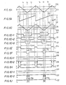
- reference numeral 11 designates a film exposing section which records an information by exposing a cinema film 14 by an electron beam 13 emitted from a cathode 12.
- the electron beam 13 is projected through a gate electrode 15 and a deflection electrode 16 to a sound track 17 ( Figure 5) of the film 14.
- a sawtooth deflection signal S2 (Figure 6B) generated from a deflection drive circuit 22 on the basis of a triangular wave signal S1 ( Figure 6A) having a high frequency (for example, 128 kHz) which is generated from a scanning signal generator 21, whereby at a predetermined cycle T1 which is the same as that of the triangular wave signal S1, the electron beam 13 is made to scan the film 14 in its width direction perpendicular to its running direction (shown by an arrow 23) to draw an exposed locus 24 ( Figure 5).
- a triangular wave signal S1 ( Figure 6A) having a high frequency (for example, 128 kHz) which is generated from a scanning signal generator 21, whereby at a predetermined cycle T1 which is the same as that of the triangular wave signal S1, the electron beam 13 is made to scan the film 14 in its width direction perpendicular to its running direction (shown by an arrow 23) to draw an exposed locus 24 ( Figure 5).
- An amplitude V ( Figure 6B) of the deflection signal S2 is selected to be such a value capable of scanning an effective width W ( Figure 5) of the sound track 17. Accordingly, the effective scanning interval formed of one cycle interval T1 of the deflection signal S2 (which is the same as the triangular wave signal S1) is made corresponding to the effective width W of the sound track 17, whereby the electron beam 13 at a time point of the effective scanning interval T1 passes over the position of substantially the central line X of the sound track 17.
- a gate drive signal S3 produced at an output terminal of a gate drive circuit 27 that is controlled by a scanning width modulating circuit 26.
- the scanning width modulating circuit 26 compares an output signal S5 ( Figure 6C), which results from gain-controlling a sound input signal S4 by a controllable gain amplifier 28, with a reference signals S6 ( Figure 6C), which results from level-converting the triangular wave signal S1 ( Figure 6A) fed from the scanning signal generator 21 and produces a scanning width control signal S7 ( Figure 6D1) which falls down to a logic "L” level and which rises up to a logic "H” level at time points t, and t 3 at which the output signal S5 intersects the reference signal S6.
- the gate drive circuit 27 generates the gate drive signal S 3 whose drive potential is increased during the interval T2 ( Figure 6D1) in which the scanning width control signal S7 falls down to the logic "L” level and of which the drive potential is decreased during other intervals in which the scanning width control signal rises up to logic "H” level.
- the potential when the gate drive signal S3 is increased is selected to be approximately the same as a potential (for example, -20 kV) of the cathode 12 of the film exposing section 11, whereby the electron beam 13 emitted from the cathode 12 travels through the gate electrode 15 and a small through-hole 30 formed through an anode 49 supplied with a high voltage (for example, +20 kV) and then reaches the film 14.
- a potential for example, -20 kV
- the potential when the gate drive signal S3 falls down is selected to be a value (for example, in the range from -30 to 50V) considerably lower than the potential of the cathode 12, whereby the electron beam 13 emitted from the cathode 12 can be returned by the gate electrode 15 so as to be prevented from passing through the small through-hole 30. Accordingly, of the effective scanning interval T1, during the interval T2 in which the scanning control signal S7 is at the logic "L" level and the gate drive signal S3 is at high potential, the electron beam 13 can pass through the gate electrode 15 and can scan and expose the film 14 but can not scan and expose it during other remaining intervals.
- the change of the falling down width T2 of the scanning width control signal S7 is produced symmetrical across a time point t 2 that corresponds to the central point of the sound track.
- the signal level of the output signal S5 is fluctuated to S51 and S52 ( Figure 6C)
- the falling-down widths T21 and T22 of the scanning width control signal S7 are symmetrically increased or decreased around the time point t 2 as shown in Figure 6D2 or 6D3.
- the scanning width control signal S7 developed at the output terminal of the scanning width modulating circuit 26 is fed to a modulation abnormality detector circuit 35 and an abnormality detecting signal S11 therefrom is fed to a detecting signal processing circuit 36.
- the modulation abnormality detector circuit 35 detects when the falling-down width T2 of the scanning width control signal S7 exceeds a predetermined upper limit value and a predetermined lower limit value and includes upper limit value and lower limit value setting circuits 37 and 38 as shown in Figure 7.
- These setting circuits 37 and 38 include comparator circuits 39 and 40 which are supplied with the triangular wave signal S6 derived from the scanning signal generator 21 at their non-inverting input terminals and upper limit and lower limit reference signals S12 and S13 are supplied to inverting input terminals of the comparator circuits 39 and 40.
- the upper limit reference signal S12 is given as the signal level of the positive voltage, from a resistance voltage dividing circuit 41 connected between a positive voltage source +Vcc and the ground, while the lower limit reference signal S13 is given as the signal level of the negative voltage from a resistance voltage dividing circuit 42 connected between a negative voltage source -Vcc and the ground.
- the level of the upper limit reference signal S12 is set to be a value corresponding to the position slightly inside the effective width W of the sound track 17 so as to remove a fear that the sound input signal S4 is increased and the exposed locus 24 exceeds the effective width W of the sound track 17.
- the level of the lower limit reference signal S13 is selected to be a value corresponding to the position slightly outside the central line X of the sound track 17 so as to prevent problems if the sound input signal S4 is decreased and the exposed locus 24 is made discontinuous at the position of the central line X.
- the upper limit value setting circuit 37 generates an upper limit setting signal S14 ( Figure 6E) which falls down to logic "L” level during an interval T3 in which the triangular wave signal S1 becomes lower than the upper limit reference signal S12, while the lower limit value setting circuit 38 generates a lower limit setting signal S15 ( Figure 6F) which falls down to logic "L” level during an interval T4 in which the triangular wave signal S1 becomes lower than the lower limit reference signal S13.
- the interval T4 of the lower limit reference signal S13 means that a limit is set at the nearby position across the central line X of the sound track 17, while the interval T3 of the upper limit setting signal S14 means that a limit is set at the position near the effective width W across the central line X of the sound track 17.
- the upper limit setting signal S14 is supplied to an upper limit verifying circuit 43 formed of a NAND circuit as one verifying input, while the lower limit setting signal S15 is inverted in logic level by an inverter 44 and then fed to a lower limit verifying circuit 45 formed of a NAND circuit as one verifying input.
- the upper limit verifying circuit 43 is supplied with another verifying input which results from inverting the scanning width control signal S7 of the scanning width modulating circuit 26 by an inverter 46.
- the lower limit verying circuit 45 is directly supplied with the scanning width control signal S7 as another verifying input thereof.
- the verifying outputs S16 and S17 from the upper limit verifying circuit 43 and the lower limit verifying circuit 45 are supplied to abnormality detecting signal generator circuits 47 and 48 each formed of a retriggerable monostable multivibrator which are triggered at the falling-down edges of the verifying outputs S16 and S17 when they fall down from logic "H" level to logic "L” level.
- abnormality detecting signal generator circuits 47 and 48 each formed of a retriggerable monostable multivibrator which are triggered at the falling-down edges of the verifying outputs S16 and S17 when they fall down from logic "H" level to logic "L” level.
- their Q outputs which become logic "L” during a predetermined limited time are supplied through a wired-OR circuit 51 to the base of a switching transistor 50 formed of a PNP type transistor in the signal processing circuit 36 as an abnormality detecting signal S18.
- the signal processing circuit 36 is provided with a display element 52 formed, for example, of an LED connected to the collector of the transistor 50. Therefore, when the transistor 50 is turned on, the display element 52 is made to flash.
- the upper limit and lower limit verifying circuits 43 and 45 both generate the verifying signals S16 and S17 of logic "H", whereby neither of abnormality detecting signal generator circuits 47 and 48 are triggered so that the abnormality detecting signal S18 is at logic "H" level, thus turning off the transistor 50. Accordingly, the detecting signal processing circuit 36 does not allow the display element 52 to be made to flash.
- the signal level of the sound input signal S4 is increased and the falling-down width of the scanning width control signal S7 is enlarged to be larger than the falling-down width T3 of the setting signal S14 from the upper limit value setting circuit 39, during the enlarged interval, the input signals to the upper limit verifying circuit 43 both rise up to logic "H” so that the verifying output S16 from the upper limit verifying circuit 43 falls down to logic "L” level ( Figure 6G2). Accordingly, the abnormality detecting signal generator circuit 47 is set, thus to turn on the transistor 50 in the signal processing circuit 36. At that time, the display element 52 is made to flash so that the operator can precisely learn that the signal level of the sound input signal S4 becomes abnormal.
- the operator changes the gain of the controllable gain amplifier circuit 28 manualy so as to reduce the scanning width T2 of the scanning width control signal S7 to a value not to exceed the upper limit value.
- the operator to manually adjust the exposure scanning width so as not to be placed in the over-modulated state under which the exposure scanning width is modulated to exceed the effective width W of the sound track 17.
- the display element 52 is made to flash thereby to enable the operator to learn of the occurrence of the abnormality. Therefore, the operator can carry out the manual adjustment to control the gain of the controllable gain amplifier circuit 28 so that the scanning width of the scanning width control signal S7 is enlarged to be a value larger than the lower limit, thus to prevent the recording level from being lowered excessively to make the exposure locus 24 discontinuous.
- the display element 52 is made to flash to inform the operator of the occurrence of the abnormality and the operator adjusts the level of the sound input signal by the manual operation
- the detecting signals from the abnormality detecting signal generator circuits 47 and 48 are directly fed back to the controllable gain amplifier 28 as the gain control signal thereby to return the signal level of the output signal S5, which will be fed to the scanning width modulating circuit 26, to the upper limit value or lower limit value. If arranged as above, the adjusting work done by the operator can be made much easier.
- the width of the scanning width control signal for the beam used to carry out the exposure recording on the film becomes wider than the predetermined upper limit value or narrower than the predetermined lower limit value, this is detected and the signal level of the input signal can be adjusted so that the exposure recording can be carried out more easily with the appropriate scanning width.
- Reference numeral 11 represents the film exposing section, 12 the cathode, 15 the gate electrode, 16 the deflection electrode, 21 the scanning signal generator, 22 the deflection drive circuit, 26 the scanning width modulating circuit, 27 the gate drive circuit, 28 the controllable gain amplifier, 35 the modulation abnormality detector circuit, 36 the detecting signal processing circuit, 37 and 38 the upper limit value and lower limit value setting circuits, respectively, 39 and 40 the comparator circuits, respectively, 43 and 45 the upper limit and lower limit verifying circuits, respectively, 47 and 48 the abnormality detecting signal generator circuits, respectively and 49 the anode.
Landscapes
- Physics & Mathematics (AREA)
- Engineering & Computer Science (AREA)
- Plasma & Fusion (AREA)
- Facsimile Scanning Arrangements (AREA)
- Optical Recording Or Reproduction (AREA)
Claims (3)
- Vorrichtung zum Aufzeichnen von Daten, bei der ein von einem übereinstimmend mit einem Eingangssignal (S4) modulierten Bezugs- Abtastbreitensteuersignal (S6) gebildeter Belichtungsstrahl (13) einen Filmstreifen (14) zum Bilden einer (spurweisen) Belichtungsfläche (6) auf dem Filstreifen abtastet wodurch das Eingangssignal (S4) auf dem Filmstreifen (14) aufgezeichnet ist, dadurch gekennzeichnet,
daß ein Modulationsabnormitätsdetektor (35, 36) das modulierte Abtastbreitensteuersignal (S7) mit einem oberen (S14) und einem unteren (S15) Grenzwert- Vorgabesignal vergliecht und erfaßt, wenn eine von dem modulierten - Abtastbreitensteuersignal (S7) angezeigte Abtastbreite größer als die von dem oberen Grenzwert- Vorgabesignal (S14) angezeigte maximale Abtastbreite oder kleiner als das unter Grenzwert-Vorgabesignal (S15) wird, und der ein das Ergebnis der Erfassung anzeigendes Detektorsignal (S18) erzeugt,
daß der Modulationsabnormitätsdetektor (35, 36) einen ersten (39) und zweiten (40) Komparator zum Erzeugen eines oberen Grenzwert- Vorgabesignals (S14) und eines unteren Grenzwert- Vorgabesignals (S15) aufweist, deren jeweiligem nichtinvertierenden Eingangsanschluß das Bezugs- - Abtastbreitensteuersignal (S6) zuführbar ist und deren jeweiliger invertierender Eingangsanschluß mit der positiven bzw. negativen Spannungsquelle (41, 42) verbindbar ist, undeine Logikschaltungsanordnung (43-48) aufweist, die das modulierte Abtastbreitensteuersignal (S7) und das obere bzw. untere Grenzwert-Vorgabesignal (S14, S15) zur Erzeugung des Detektorsignals (S18) empfängt, unddaß die Logikschaltungsanordnung (43-48) aufweist:einen ersten Inverter (46) zum Empfang des modulierten Abtastbreitensteuersignal (S7),einen zweiten Inverter (44) zum Empfang des unteren Grenzwert- Vorgabesignals (S15) des zweiten Komparators (40),eine erstes NAND-Glied (43) zum Empfang des oberen Grenzwert- Vorgabesignal (S14) des ersten Komparators (39) und des Ausgangssignals des ersten Inverters (46),ein zweites NAND-Glied (45) zum Empfang des modulierten Abtastbreitensteuersignal (S7) und das Ausgangssignals des zweiten Inverters (44) undeinen ersten und einen zweiten monostabilen Multivibrator (47, 48), die zum Triggern mit den Ausgängen der ersten bzw. zweiten NAND-Glieder (43, 45) verbunden sind und deren Ausgangssignale zur Bildung des Detektorsignals (S18) addiert werden.
Applications Claiming Priority (1)
| Application Number | Priority Date | Filing Date | Title |
|---|---|---|---|
| PCT/JP1984/000261 WO1985005485A1 (fr) | 1984-05-23 | 1984-05-23 | Appareil d'enregistrement de donnees |
Publications (3)
| Publication Number | Publication Date |
|---|---|
| EP0190349A1 EP0190349A1 (de) | 1986-08-13 |
| EP0190349A4 EP0190349A4 (de) | 1987-09-10 |
| EP0190349B1 true EP0190349B1 (de) | 1989-10-25 |
Family
ID=13818332
Family Applications (1)
| Application Number | Title | Priority Date | Filing Date |
|---|---|---|---|
| EP84902064A Expired EP0190349B1 (de) | 1984-05-23 | 1984-05-23 | Vorrichtung zum speichern von daten |
Country Status (4)
| Country | Link |
|---|---|
| US (1) | US4757490A (de) |
| EP (1) | EP0190349B1 (de) |
| DE (1) | DE3480304D1 (de) |
| WO (1) | WO1985005485A1 (de) |
Families Citing this family (1)
| Publication number | Priority date | Publication date | Assignee | Title |
|---|---|---|---|---|
| DE3777461D1 (de) * | 1986-06-20 | 1992-04-23 | Matsushita Electric Industrial Co Ltd | Optisches aufzeichnungs-und wiedergabegeraet. |
Family Cites Families (11)
| Publication number | Priority date | Publication date | Assignee | Title |
|---|---|---|---|---|
| US1975279A (en) * | 1932-07-13 | 1934-10-02 | Jr Theodore Lindenberg | Apparatus for recording sound on photographic films |
| US2224914A (en) * | 1939-04-29 | 1940-12-17 | Rca Corp | Noise reduction circuit for sound recording |
| US2468047A (en) * | 1945-11-17 | 1949-04-26 | Rca Corp | Negative-positive recording method and system |
| US3197574A (en) * | 1962-04-16 | 1965-07-27 | Edgar C Zane | Noise suppression system |
| JPS4990515A (de) * | 1972-12-27 | 1974-08-29 | ||
| DE2439181A1 (de) * | 1974-08-16 | 1976-02-26 | Braun Ag | Tonaussteuerungsanzeige fuer eine tonfilmkamera |
| US4076969A (en) * | 1975-04-07 | 1978-02-28 | Singer & Singer | Impulse noise reduction system |
| JPS52102701A (en) * | 1976-02-24 | 1977-08-29 | Nippon Hoso Kyokai <Nhk> | Optical recording system |
| JPS5384505A (en) * | 1976-12-29 | 1978-07-26 | Fujitsu Ltd | Information signal superposing system for audio signal |
| JPS53116804A (en) * | 1977-03-23 | 1978-10-12 | Toshiba Corp | Signal recording and reproducing system of optical type |
| JPS5468202A (en) * | 1977-11-10 | 1979-06-01 | Sony Corp | Reproducing method of optical recording signal |
-
1984
- 1984-05-23 EP EP84902064A patent/EP0190349B1/de not_active Expired
- 1984-05-23 DE DE8484902064T patent/DE3480304D1/de not_active Expired
- 1984-05-23 US US06/823,503 patent/US4757490A/en not_active Expired - Lifetime
- 1984-05-23 WO PCT/JP1984/000261 patent/WO1985005485A1/ja not_active Ceased
Also Published As
| Publication number | Publication date |
|---|---|
| EP0190349A4 (de) | 1987-09-10 |
| EP0190349A1 (de) | 1986-08-13 |
| DE3480304D1 (en) | 1989-11-30 |
| US4757490A (en) | 1988-07-12 |
| WO1985005485A1 (fr) | 1985-12-05 |
Similar Documents
| Publication | Publication Date | Title |
|---|---|---|
| EP0044072B1 (de) | Gerät und Verfahren zum Regeln der Fokussierung in einem Aufzeichnungssystem | |
| KR880001174B1 (ko) | 디스크형 기록캐리어 판독장치 | |
| US4475182A (en) | Focus servo control system for automatically adjusting a relative distance between an objective lens unit and a recording surface of an optical recording medium | |
| US5095470A (en) | Capacitance detection control circuit for positioning a magnetic head close to a magneto-optical disk | |
| EP0164642A2 (de) | Aufzeichnungs- und Wiedergabegerät | |
| KR0146293B1 (ko) | 광학주사장치 | |
| US3567855A (en) | Scanning apparatus with automatic beam centering | |
| US4068197A (en) | Apparatus for stabilizing beam for exposure | |
| KR0169103B1 (ko) | 광 검출 가능한 정보 패턴을 레코드 캐리어에 레코딩하는 레코딩 장치 | |
| CA1195424A (en) | Control circuitry for preliminary focusing of light on a record medium surface in an optical reproducing apparatus | |
| CA1051549A (en) | Arrangement for aligning the image of an information structure on a converter | |
| KR850001654B1 (ko) | 기록시스템에서의 촛점 조절장치 | |
| EP0190349B1 (de) | Vorrichtung zum speichern von daten | |
| JPS6321167B2 (de) | ||
| GB2110434A (en) | Apparatus for scanning a disc-shaped record carrier | |
| EP0352137B1 (de) | Pulsbreitenmodulator und Treiberschaltung mit diesem Modulator | |
| KR0185173B1 (ko) | 자동 서보 이득 제어 시스템 | |
| US2840720A (en) | Multiplier phototube stabilizing circuit | |
| JPS59174069A (ja) | レ−ザダイオ−ド制御回路 | |
| JPS6244943A (ja) | 電子線露光装置 | |
| JPH0467254B2 (de) | ||
| JPH04147208A (ja) | レーザ書込装置 | |
| US2468047A (en) | Negative-positive recording method and system | |
| US4716384A (en) | Modulators | |
| US4734903A (en) | Level control circuit for light beam recording apparatus |
Legal Events
| Date | Code | Title | Description |
|---|---|---|---|
| PUAI | Public reference made under article 153(3) epc to a published international application that has entered the european phase |
Free format text: ORIGINAL CODE: 0009012 |
|
| 17P | Request for examination filed |
Effective date: 19860515 |
|
| AK | Designated contracting states |
Kind code of ref document: A1 Designated state(s): DE FR GB NL |
|
| A4 | Supplementary search report drawn up and despatched |
Effective date: 19870910 |
|
| 17Q | First examination report despatched |
Effective date: 19880413 |
|
| GRAA | (expected) grant |
Free format text: ORIGINAL CODE: 0009210 |
|
| AK | Designated contracting states |
Kind code of ref document: B1 Designated state(s): DE FR GB NL |
|
| REF | Corresponds to: |
Ref document number: 3480304 Country of ref document: DE Date of ref document: 19891130 |
|
| ET | Fr: translation filed | ||
| PLBE | No opposition filed within time limit |
Free format text: ORIGINAL CODE: 0009261 |
|
| STAA | Information on the status of an ep patent application or granted ep patent |
Free format text: STATUS: NO OPPOSITION FILED WITHIN TIME LIMIT |
|
| 26N | No opposition filed | ||
| REG | Reference to a national code |
Ref country code: GB Ref legal event code: IF02 |
|
| PGFP | Annual fee paid to national office [announced via postgrant information from national office to epo] |
Ref country code: FR Payment date: 20030508 Year of fee payment: 20 |
|
| PGFP | Annual fee paid to national office [announced via postgrant information from national office to epo] |
Ref country code: GB Payment date: 20030519 Year of fee payment: 20 |
|
| PGFP | Annual fee paid to national office [announced via postgrant information from national office to epo] |
Ref country code: NL Payment date: 20030530 Year of fee payment: 20 |
|
| PGFP | Annual fee paid to national office [announced via postgrant information from national office to epo] |
Ref country code: DE Payment date: 20030605 Year of fee payment: 20 |
|
| PG25 | Lapsed in a contracting state [announced via postgrant information from national office to epo] |
Ref country code: GB Free format text: LAPSE BECAUSE OF EXPIRATION OF PROTECTION Effective date: 20040522 |
|
| PG25 | Lapsed in a contracting state [announced via postgrant information from national office to epo] |
Ref country code: NL Free format text: LAPSE BECAUSE OF EXPIRATION OF PROTECTION Effective date: 20040523 |
|
| REG | Reference to a national code |
Ref country code: GB Ref legal event code: PE20 |
|
| NLV7 | Nl: ceased due to reaching the maximum lifetime of a patent |
Effective date: 20040523 |