EP0187580A1 - Gehäuse für ein mit einem Wasserumlauf gekühltes Hochfrequenzleistungselement - Google Patents
Gehäuse für ein mit einem Wasserumlauf gekühltes Hochfrequenzleistungselement Download PDFInfo
- Publication number
- EP0187580A1 EP0187580A1 EP85402435A EP85402435A EP0187580A1 EP 0187580 A1 EP0187580 A1 EP 0187580A1 EP 85402435 A EP85402435 A EP 85402435A EP 85402435 A EP85402435 A EP 85402435A EP 0187580 A1 EP0187580 A1 EP 0187580A1
- Authority
- EP
- European Patent Office
- Prior art keywords
- housing
- window
- main body
- plate
- electrodes
- Prior art date
- Legal status (The legal status is an assumption and is not a legal conclusion. Google has not performed a legal analysis and makes no representation as to the accuracy of the status listed.)
- Withdrawn
Links
Images

Classifications
-
- H—ELECTRICITY
- H05—ELECTRIC TECHNIQUES NOT OTHERWISE PROVIDED FOR
- H05K—PRINTED CIRCUITS; CASINGS OR CONSTRUCTIONAL DETAILS OF ELECTRIC APPARATUS; MANUFACTURE OF ASSEMBLAGES OF ELECTRICAL COMPONENTS
- H05K5/00—Casings, cabinets or drawers for electric apparatus
- H05K5/0091—Housing specially adapted for small components
-
- H—ELECTRICITY
- H01—ELECTRIC ELEMENTS
- H01L—SEMICONDUCTOR DEVICES NOT COVERED BY CLASS H10
- H01L23/00—Details of semiconductor or other solid state devices
- H01L23/34—Arrangements for cooling, heating, ventilating or temperature compensation ; Temperature sensing arrangements
- H01L23/46—Arrangements for cooling, heating, ventilating or temperature compensation ; Temperature sensing arrangements involving the transfer of heat by flowing fluids
- H01L23/473—Arrangements for cooling, heating, ventilating or temperature compensation ; Temperature sensing arrangements involving the transfer of heat by flowing fluids by flowing liquids
-
- H—ELECTRICITY
- H01—ELECTRIC ELEMENTS
- H01L—SEMICONDUCTOR DEVICES NOT COVERED BY CLASS H10
- H01L23/00—Details of semiconductor or other solid state devices
- H01L23/58—Structural electrical arrangements for semiconductor devices not otherwise provided for, e.g. in combination with batteries
- H01L23/64—Impedance arrangements
- H01L23/66—High-frequency adaptations
-
- H—ELECTRICITY
- H05—ELECTRIC TECHNIQUES NOT OTHERWISE PROVIDED FOR
- H05K—PRINTED CIRCUITS; CASINGS OR CONSTRUCTIONAL DETAILS OF ELECTRIC APPARATUS; MANUFACTURE OF ASSEMBLAGES OF ELECTRICAL COMPONENTS
- H05K7/00—Constructional details common to different types of electric apparatus
- H05K7/20—Modifications to facilitate cooling, ventilating, or heating
-
- H—ELECTRICITY
- H01—ELECTRIC ELEMENTS
- H01L—SEMICONDUCTOR DEVICES NOT COVERED BY CLASS H10
- H01L2924/00—Indexing scheme for arrangements or methods for connecting or disconnecting semiconductor or solid-state bodies as covered by H01L24/00
- H01L2924/0001—Technical content checked by a classifier
- H01L2924/0002—Not covered by any one of groups H01L24/00, H01L24/00 and H01L2224/00
-
- H—ELECTRICITY
- H05—ELECTRIC TECHNIQUES NOT OTHERWISE PROVIDED FOR
- H05K—PRINTED CIRCUITS; CASINGS OR CONSTRUCTIONAL DETAILS OF ELECTRIC APPARATUS; MANUFACTURE OF ASSEMBLAGES OF ELECTRICAL COMPONENTS
- H05K1/00—Printed circuits
- H05K1/18—Printed circuits structurally associated with non-printed electric components
- H05K1/182—Printed circuits structurally associated with non-printed electric components associated with components mounted in the printed circuit board, e.g. insert mounted components [IMC]
Definitions
- the invention relates to power component housings which must operate at high frequency.
- the present invention provides a new housing structure allowing a very good compromise as defined above.
- This structure adapts to the encapsulation of a single component or of several components in the same housing.
- the housing includes a thermally conductive main body, provided with a cavity intended to accommodate at least one component, as well as recesses formed in the main body and access openings to these recesses for introducing and evacuating a circulating cooling fluid. forced; on a part of its periphery, the main body is provided with a rim in projection having a flat bottom surface constituting a bearing surface when the body of the housing is inserted in a window cut out from a printed circuit board; on another part of the periphery of the main body, planar electrodes come out of the cavity, in which they are connected to the component, these electrodes having their underside situated in the plane of said bearing surface so that when the body of the housing is inserted in said window the electrodes come to bear against connections printed on the plate, connections which substantially end at the edge of the window drilled in the plate; finally, the access openings to the recesses are placed below the plane of the bearing surface and at a sufficient distance from this plane so that it is possible, when the body of the housing is placed in
- the openings are located in one face of the main body parallel or perpendicular to the planar bearing surface and the conduits which are connected to it exit perpendicular to this face.
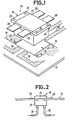
- FIG 1 there is shown in perspective the housing 10 according to the invention, placed above a printed circuit board 12 on which this housing is to be mounted.
- the housing has a generally parallelepiped shape and it is intended to be inserted in a rectangular window 14 cut out from the printed circuit board 12. It is also intended to be fixed to this plate in principle by bolts or rivets passing through circular openings 16 drilled near the window 14.
- Printed connections 18 arrive near the window 14 and it is to these connections that the power component (or the power components) enclosed in the housing 10 must be electrically connected. example four printed connections. These connections make it possible to connect the component (s) to other elements of the printed circuit.
- the housing 10 comprises a main body 20 of heat conducting material (copper for example) because, in addition to its role of protecting the component which it contains, it plays the role of dissipator of the heat generated in the component.
- the main body has a cavity in which is housed the component or components. This cavity is not visible in the external view of FIG. 1, but there is a cover 22 which closes it in the example shown. It is for example a cover of electrically insulating protective resin, injected into the cavity to drown the component.
- the lower part of the main body 20 has dimensions corresponding substantially to those of the window 14 so that it can be inserted into this window.
- This lower part is here rectangular.
- the upper part also comprises, on a part of its periphery, a protruding rim 24 (here a rim on one side of the rectangle and another rim on an opposite side of the rectangle).
- the protruding rim 24 has a flat lower face defining a bearing surface, which comes to bear on the edges of the window 14 cut out in the printed circuit board 12 when the main body 20 is inserted in this window.
- the rim 24 is pierced with circular openings 26 of dimensions and positions adapted to those of the openings 16 of the printed circuit board, to allow solid fixing of the housing against the plate.
- planar metal electrodes emerge, here four electrodes 28. These electrodes exit from a part of the main body 20 not provided with a projecting rim 24. They are coplanar and the plane of their lower surface coincides with the plane of the bearing surface formed by the underside of the projecting rim 24.
- the lateral positions of the different electrodes 28 correspond to the positions of the printed connections 18 of the plate 12; when the housing is fixed on the plate, the projecting edges are applied tightly against the edges of the window 14 and the planar electrodes 28 are applied closely each against a respective connection 18, ensuring an effective electrical connection in the same plane, of two flat conductors.
- the main body 20 of the housing has internal recesses not visible in Figure 1, intended to ensure circulation of a coolant put into forced circulation. These recesses open to the outside of the body 20 on openings (in principle a fluid supply opening and a discharge opening) which can be connected to fluid circulation conduits.
- the openings are placed below the plane of the support surface of the flanges 24 and therefore the plane of the underside of the electrodes 28, at a sufficient distance from this plane so that when the housing is placed on the plate 12 the openings and the conduits which are connected thereto are located below the plate 12 (while the electrodes are above).
- FIG. 2 shows a side view of the housing 10 mounted on the plate, with the electrodes 28 which rest on the plate and forced circulation conduits 30 (inlet) and 32 (outlet) connected respectively to a fluid supply opening and a fluid discharge opening which in this case faces downward; instead of being drilled in the lower face of the housing (face parallel to the plane of the electrodes), these openings could be formed in the lateral faces, but far enough from the plane of the lower surface of the plate 12 so that the conduits can be easily placed below the plate.
- Figures 3 to 5 show, respectively in cross section, in longitudinal section and in top view of the main body of the housing; the component, and the resin which drowns the component and closes the cavity in which the component is housed, have not been shown in these figures, as have the external connection electrodes.
- the recesses are here made by horizontal holes (longitudinal and transverse) and vertical holes. These holes cut each other and therefore form paths communication capable of allowing the circulation of a cooling fluid between two external openings.
- two parallel horizontal channels 34 and 36 drilled in a direction which will be called longitudinal, opening out through two respective external openings 38 and 40.
- the section of FIG. 3 is made through the channel 36.
- a horizontal channel 42 drilled in a transverse direction makes communicate, at their end opposite to the openings 38 and 40, the longitudinal channels 34 and 36.
- This channel 42 leads to an opening 44.
- Two vertical channels 46 and 48 can also be drilled from the lower surface from the main body towards the longitudinal channels 34 and 36 towards their ends on the side of the openings 38 and 40. These channels 46 and 48 open onto the lower face of the body 20 through openings 50 and 52 respectively.
- the openings 38 and 40 as well as the openings (50. and 52) are situated far below the plane of the bearing surface (lower face) of the projecting flanges 24.
- the openings of the various channels are threaded so that they can be fixed therein. either a plug (in particular in the opening 44), or a connection fitting for a supply or evacuation pipe for fluid in forced circulation.
- the openings 38 and 40 are plugged and the openings 50 and 52 are connected to conduits; the opposite can also be done, namely plugging the openings 50 and 52 and connecting conduits to the openings 38 and 40.
- FIG. 6 The elements intended to come inside the cavity are shown in FIG. 6 in the case of a single component with four connections (four electrodes on the front face of the chip constituting the component and one electrode on the rear face).
- the chip is designated by the reference 56. It is generally soldered by its rear face on a conductive track printed with an insulating plate 58. The chip is electrically connected to pads 60, 62, 64, 66 which themselves are connected by wires welded to conductive electrodes 28 cut from a metal plate.
- the front part of the electrodes projects beyond the housing on the sides which are not surrounded by the projecting rim 24.
- a peripheral holding frame not shown which will be cut to isolate the electrodes from each other at the end of mounting (frame of dimensions greater than those of the housing).
- the electrodes are put in place and the connecting wires are welded after which a protective resin is then put in place to close the cavity 54.
- thermally conductive (alumina) plates can be provided between the bottom of the cavity 54 and the printed support plate 58.
- the total thickness of the elements installed in the cavity 54 must be such that the lower surface of the electrodes is flush with the plane of the lower surface of the protruding flange 24.
Landscapes
- Engineering & Computer Science (AREA)
- Microelectronics & Electronic Packaging (AREA)
- Physics & Mathematics (AREA)
- Condensed Matter Physics & Semiconductors (AREA)
- General Physics & Mathematics (AREA)
- Computer Hardware Design (AREA)
- Power Engineering (AREA)
- Thermal Sciences (AREA)
- Cooling Or The Like Of Electrical Apparatus (AREA)
- Cooling Or The Like Of Semiconductors Or Solid State Devices (AREA)
Applications Claiming Priority (2)
| Application Number | Priority Date | Filing Date | Title |
|---|---|---|---|
| FR8418927 | 1984-12-11 | ||
| FR8418927A FR2574615B1 (fr) | 1984-12-11 | 1984-12-11 | Boitier pour composant de puissance haute-frequence refroidi par circulation d'eau |
Publications (1)
| Publication Number | Publication Date |
|---|---|
| EP0187580A1 true EP0187580A1 (de) | 1986-07-16 |
Family
ID=9310479
Family Applications (1)
| Application Number | Title | Priority Date | Filing Date |
|---|---|---|---|
| EP85402435A Withdrawn EP0187580A1 (de) | 1984-12-11 | 1985-12-06 | Gehäuse für ein mit einem Wasserumlauf gekühltes Hochfrequenzleistungselement |
Country Status (3)
| Country | Link |
|---|---|
| US (1) | US4622621A (de) |
| EP (1) | EP0187580A1 (de) |
| FR (1) | FR2574615B1 (de) |
Cited By (1)
| Publication number | Priority date | Publication date | Assignee | Title |
|---|---|---|---|---|
| EP0334747A1 (de) * | 1988-03-25 | 1989-09-27 | Thomson Hybrides Et Microondes | Vorrichtung zur Verbindung und für den Schutz eines unbedeckten Chips eines Hochfrequenzbauteils |
Families Citing this family (12)
| Publication number | Priority date | Publication date | Assignee | Title |
|---|---|---|---|---|
| FR2587857B1 (fr) * | 1985-09-24 | 1987-12-24 | Centre Nat Rech Scient | Oscillateur thermostate miniature |
| US4731693A (en) * | 1986-09-29 | 1988-03-15 | Tektronix, Inc. | Connection apparatus for integrated circuit |
| US4871623A (en) * | 1988-02-19 | 1989-10-03 | Minnesota Mining And Manufacturing Company | Sheet-member containing a plurality of elongated enclosed electrodeposited channels and method |
| US5070606A (en) * | 1988-07-25 | 1991-12-10 | Minnesota Mining And Manufacturing Company | Method for producing a sheet member containing at least one enclosed channel |
| US6031726A (en) * | 1995-11-06 | 2000-02-29 | Vlt Corporation | Low profile mounting of power converters with the converter body in an aperture |
| AU7596698A (en) * | 1997-05-23 | 1998-12-11 | Alpine Microsystems, Inc. | A system and method for packaging integrated circuits |
| US6234842B1 (en) | 1998-11-20 | 2001-05-22 | Vlt Corporation | Power converter connector assembly |
| FR2809281B1 (fr) * | 2000-05-22 | 2002-07-12 | Alstom | Dispositif electronique de puissance |
| US6434005B1 (en) | 2000-10-27 | 2002-08-13 | Vlt Corporation | Power converter packaging |
| ES2177447B1 (es) * | 2000-12-29 | 2004-08-16 | Lear Automotive (Eeds) Spain, S.L. | Circuito electronico con terminales de conexion integrados y metodo para su fabricacion. |
| US7361844B2 (en) * | 2002-11-25 | 2008-04-22 | Vlt, Inc. | Power converter package and thermal management |
| CN101651445A (zh) * | 2009-09-02 | 2010-02-17 | 东莞市大普通信技术有限公司 | 恒温晶体振荡器 |
Citations (4)
| Publication number | Priority date | Publication date | Assignee | Title |
|---|---|---|---|---|
| FR2316737A1 (fr) * | 1975-07-02 | 1977-01-28 | Honeywell Inf Systems | Echangeur de chaleur pour circuits electroniques |
| US4079410A (en) * | 1975-12-10 | 1978-03-14 | Semikron Gesellschaft Fur Gleichrichterbau Und Elektronik M.B.H. | Semiconductor rectifier device with improved cooling arrangement |
| US4341432A (en) * | 1979-08-06 | 1982-07-27 | Cutchaw John M | Liquid cooled connector for integrated circuit packages |
| US4504886A (en) * | 1983-02-28 | 1985-03-12 | Motorola Inc. | Grounding and positioning clip for a power transistor |
Family Cites Families (3)
| Publication number | Priority date | Publication date | Assignee | Title |
|---|---|---|---|---|
| US3741292A (en) * | 1971-06-30 | 1973-06-26 | Ibm | Liquid encapsulated air cooled module |
| US4216488A (en) * | 1978-07-31 | 1980-08-05 | Hutson Jearld L | Lateral semiconductor diac |
| US4577402A (en) * | 1984-06-13 | 1986-03-25 | Penn Engineering & Manufacturing Corp. | Stud for mounting and method of mounting heat sinks on printed circuit boards |
-
1984
- 1984-12-11 FR FR8418927A patent/FR2574615B1/fr not_active Expired
-
1985
- 1985-12-06 EP EP85402435A patent/EP0187580A1/de not_active Withdrawn
- 1985-12-09 US US06/807,019 patent/US4622621A/en not_active Expired - Lifetime
Patent Citations (4)
| Publication number | Priority date | Publication date | Assignee | Title |
|---|---|---|---|---|
| FR2316737A1 (fr) * | 1975-07-02 | 1977-01-28 | Honeywell Inf Systems | Echangeur de chaleur pour circuits electroniques |
| US4079410A (en) * | 1975-12-10 | 1978-03-14 | Semikron Gesellschaft Fur Gleichrichterbau Und Elektronik M.B.H. | Semiconductor rectifier device with improved cooling arrangement |
| US4341432A (en) * | 1979-08-06 | 1982-07-27 | Cutchaw John M | Liquid cooled connector for integrated circuit packages |
| US4504886A (en) * | 1983-02-28 | 1985-03-12 | Motorola Inc. | Grounding and positioning clip for a power transistor |
Cited By (1)
| Publication number | Priority date | Publication date | Assignee | Title |
|---|---|---|---|---|
| EP0334747A1 (de) * | 1988-03-25 | 1989-09-27 | Thomson Hybrides Et Microondes | Vorrichtung zur Verbindung und für den Schutz eines unbedeckten Chips eines Hochfrequenzbauteils |
Also Published As
| Publication number | Publication date |
|---|---|
| FR2574615B1 (fr) | 1987-01-16 |
| FR2574615A1 (fr) | 1986-06-13 |
| US4622621A (en) | 1986-11-11 |
Similar Documents
| Publication | Publication Date | Title |
|---|---|---|
| EP0187580A1 (de) | Gehäuse für ein mit einem Wasserumlauf gekühltes Hochfrequenzleistungselement | |
| EP0338477B1 (de) | Gehäuse für Unterwassereinrichtung | |
| FR2569309A1 (fr) | Connecteur pour plaque de base | |
| EP1158656A1 (de) | Elektronische Leistungsvorrichtung | |
| EP3551501B1 (de) | Wärmeableitungsvorrichtung für eine multimedia-steuereinheit | |
| EP3375266A1 (de) | Elektrische sammelschiene | |
| EP3621093B1 (de) | Kapazitiver block mit einem kühlkörper | |
| FR2930848A3 (fr) | Prise electrique multiple de securite | |
| FR3043879A1 (fr) | Ensemble formant boitier pour un equipement electrique | |
| EP0047195A2 (de) | Kunststoffgehäuse für integrierte Schaltungen | |
| WO2017081256A1 (fr) | Boitier pour un equipement electrique | |
| WO2003051095A1 (fr) | Module de puissance et ensemble de modules de puissance | |
| EP1912261A1 (de) | Elektrische Anschlussvorrichtung, insbesondere für elektrischen Sonnenkollektor | |
| EP2745661B1 (de) | Elektrische verbindungsvorrichtung, anordnung mit einer solchen vorrichtung und elektronikplatine sowie verfahren zum elektrischen anschluss einer elektronikplatine | |
| WO2017081243A1 (fr) | Ensemble formant boitier pour un equipement electrique | |
| EP1054445A1 (de) | Elektronisches Gehäuse auf einer Leiterplatte sowie Verfahren zu seiner Herstellung | |
| FR2551268A1 (fr) | Monture de pile electrique horizontale, pour piles cylindriques | |
| EP2477253A1 (de) | Vorrichtung zur Aufnahme einer Vielzahl von Batterien | |
| EP0947378A1 (de) | Vorrichtung zur Kühlung von elektronischem Leistungssystem | |
| EP0911932B1 (de) | Montageadapter für nichtquadratisch geformtes elektrisches Apparat | |
| FR2928784A1 (fr) | Dispositif de raccordement electrique notamment pour panneau solaire electrique | |
| EP3549164B1 (de) | Vorrichtung zur beseitigung von wärme | |
| EP4338560A1 (de) | Spannungswandlungssystem und verfahren zur herstellung solch eines spannungswandlungssystems | |
| FR2605481A1 (fr) | Dispositif de refroidissement de composants electriques de puissance disposes dans un tiroir embrochable dans une baie | |
| FR2822341A1 (fr) | Dispositif electronique avec drain thermique |
Legal Events
| Date | Code | Title | Description |
|---|---|---|---|
| PUAI | Public reference made under article 153(3) epc to a published international application that has entered the european phase |
Free format text: ORIGINAL CODE: 0009012 |
|
| AK | Designated contracting states |
Kind code of ref document: A1 Designated state(s): DE FR GB NL |
|
| 17P | Request for examination filed |
Effective date: 19860807 |
|
| 17Q | First examination report despatched |
Effective date: 19880322 |
|
| STAA | Information on the status of an ep patent application or granted ep patent |
Free format text: STATUS: THE APPLICATION IS DEEMED TO BE WITHDRAWN |
|
| 18D | Application deemed to be withdrawn |
Effective date: 19880817 |
|
| RIN1 | Information on inventor provided before grant (corrected) |
Inventor name: BARRE, LUCIEN |