EP0187226A2 - Sputtering apparatus with film forming directivity - Google Patents
Sputtering apparatus with film forming directivity Download PDFInfo
- Publication number
- EP0187226A2 EP0187226A2 EP85114424A EP85114424A EP0187226A2 EP 0187226 A2 EP0187226 A2 EP 0187226A2 EP 85114424 A EP85114424 A EP 85114424A EP 85114424 A EP85114424 A EP 85114424A EP 0187226 A2 EP0187226 A2 EP 0187226A2
- Authority
- EP
- European Patent Office
- Prior art keywords
- sputtering
- target
- film
- substrate
- particles
- Prior art date
- Legal status (The legal status is an assumption and is not a legal conclusion. Google has not performed a legal analysis and makes no representation as to the accuracy of the status listed.)
- Granted
Links
Images


Classifications
-
- C—CHEMISTRY; METALLURGY
- C23—COATING METALLIC MATERIAL; COATING MATERIAL WITH METALLIC MATERIAL; CHEMICAL SURFACE TREATMENT; DIFFUSION TREATMENT OF METALLIC MATERIAL; COATING BY VACUUM EVAPORATION, BY SPUTTERING, BY ION IMPLANTATION OR BY CHEMICAL VAPOUR DEPOSITION, IN GENERAL; INHIBITING CORROSION OF METALLIC MATERIAL OR INCRUSTATION IN GENERAL
- C23C—COATING METALLIC MATERIAL; COATING MATERIAL WITH METALLIC MATERIAL; SURFACE TREATMENT OF METALLIC MATERIAL BY DIFFUSION INTO THE SURFACE, BY CHEMICAL CONVERSION OR SUBSTITUTION; COATING BY VACUUM EVAPORATION, BY SPUTTERING, BY ION IMPLANTATION OR BY CHEMICAL VAPOUR DEPOSITION, IN GENERAL
- C23C14/00—Coating by vacuum evaporation, by sputtering or by ion implantation of the coating forming material
- C23C14/22—Coating by vacuum evaporation, by sputtering or by ion implantation of the coating forming material characterised by the process of coating
- C23C14/34—Sputtering
-
- H—ELECTRICITY
- H01—ELECTRIC ELEMENTS
- H01J—ELECTRIC DISCHARGE TUBES OR DISCHARGE LAMPS
- H01J37/00—Discharge tubes with provision for introducing objects or material to be exposed to the discharge, e.g. for the purpose of examination or processing thereof
- H01J37/32—Gas-filled discharge tubes
- H01J37/34—Gas-filled discharge tubes operating with cathodic sputtering
- H01J37/3411—Constructional aspects of the reactor
- H01J37/3414—Targets
- H01J37/3423—Shape
-
- H—ELECTRICITY
- H01—ELECTRIC ELEMENTS
- H01J—ELECTRIC DISCHARGE TUBES OR DISCHARGE LAMPS
- H01J37/00—Discharge tubes with provision for introducing objects or material to be exposed to the discharge, e.g. for the purpose of examination or processing thereof
- H01J37/32—Gas-filled discharge tubes
- H01J37/34—Gas-filled discharge tubes operating with cathodic sputtering
- H01J37/3402—Gas-filled discharge tubes operating with cathodic sputtering using supplementary magnetic fields
- H01J37/3405—Magnetron sputtering
- H01J37/3408—Planar magnetron sputtering
-
- H—ELECTRICITY
- H01—ELECTRIC ELEMENTS
- H01J—ELECTRIC DISCHARGE TUBES OR DISCHARGE LAMPS
- H01J2237/00—Discharge tubes exposing object to beam, e.g. for analysis treatment, etching, imaging
- H01J2237/32—Processing objects by plasma generation
- H01J2237/33—Processing objects by plasma generation characterised by the type of processing
- H01J2237/332—Coating
- H01J2237/3322—Problems associated with coating
- H01J2237/3327—Coating high aspect ratio workpieces
Definitions
- the present invention relates to a planar magnetron sputtering apparatus which forms a thin film by the use of sputtering. More particularly, it relates to a sputtering apparatus of good step coverage by which a substrate to be formed with a film and having a microscopic through-hole or the like as the shape of a stepped part can be formed with the thin film faithfully to the shape.
- a conventional planar magnetron sputtering process is described in detail in, for example, a paper by JHON L. VOSSEN, WERNER KERN et al. contained in "Thin Film Processes", ACADEMIC PRESS, 1978.
- a material to be sputtered is sputtered and scattered by an inert atomic species heavier than a hydrogen atom, such as Ar, thereby to reach a substrate on which a film is to be formed.
- the directions of the scattering, are controlled according to the cosine law. Therefore, when a stepped part exits on the substrate to be formed with the film, overhangs are formed on the side walls of the step.
- the actual film formation by the sputtering is employed for the production of semiconductor devices (ICs, LSIs, etc.) and various thin-film modules (thermal recording heads, etc.). More concretely, it is important as a technique for forming an interconnection layer, a conductor layer and an insulator layer.
- An object of the present invention is to provide an apparatus which performs sputtering film formation of favorable step coverage. More in detail, it is to provide a planar magnetron sputtering apparatus in which, in order to form a film on a stepped portion having a microscopic through-hole as per the shape of the underlying step, sputtering particles with a directivity are caused to fly onto a substrate for the film formation, thereby making it possible to form the film faithfully to the shape of the step.
- the present invention is characterized in that inferior film formation coverage attributed to the government of the emission angle distribution of sputtering particles by the cosine law is improved by positively limiting part of the emissive angular extent. That is, the flights of the sputtering particles are physically limi.ted on the side of the emission source of the sputtering particles or/and the side of a substrate to be formed with a film.
- a glow discharge In a sputtering apparatus, a glow discharge must be maintained within a space of reduced pressure. An electron generated by the discharge performs a helical motion so as to wind round a magnetic field vector /B (Fig. 20). Therefore, the mean free path (hereinbelow, abbreviated to 'mfp') of the electron lengthens. This effect increases the probability of the collision of the electron with the particles of a sputtering gas (usually, the particles of an inert gas such as argon gas); to generate an intense glow discharge.
- a sputtering gas usually, the particles of an inert gas such as argon gas
- This electron performs the magnetron motion also in the bottom portion of the hole. More specifically, when the electron 101 has approached a hole side wall 201, it is repelled by the electric field of the target at a great minus potential and is pushed back in the direction opposite to that of the magnetron motion. However, the electron is advanced toward the hole side wall 201 by the force of the magnetron motion again, whereupon it is pushed back under the repulsive force of the electric field again. It continues such motions. Therefore, the mfp enlarges, and the intense glow discharge can be sustained even under a pressure of or below 10 3 Torr which is a pressure atmosphere in ordinary sputtering.
- the discharge concentrates in the hole bottom portion, it concentrates in the hole, and the sputtering phenomenon is induced by the gas ionized plus within the hole.
- the sputtering particles which are emitted according to the ordinary cosine law within the hole have the emission angle distribution thereof limited in accordance with a solid angle defined when a space above the principal surface of the target is viewed from within the hole.
- Fig. 22 illustrates that the angle of emission of sputtering particles from one point of the hole bottom conforms with the cosine law if side walls are not provided, but that the sputtering particles are blocked by the hole side walls 201 and 203 to undergo an angular distribution.
- the hole side walls 201 and 203 are accordingly consumed by sputtering, but the particles sputtered from the hole bottom deposit thereon, so that the open diameter of the hole does not enlarge due to the sputtering. Therefore, the directivity imparted to the sputtering particles remains unchanged, and none of an overhang shape etc. arises on the stepped portion of a substrate for film formation at all times, so that favorable film characteristics can be maintained.
- the inferior step coverage of the stepped portion is attributed to the fact that the entrance of the sputtering particles on the substrate conforms with the cosine law. That is, the sputtering particles entering the substrate perpendicularly are smaller in number than the particles entering the same at any other angles, so that overhangs are formed on the stepped portion to worsen the step coverage.
- a target material is sputtered from a sputtering target 1 to a wafer 2.
- This wafer is previously formed with a first layer of interconnection 3, an inter-layer insulator film 4, and through-holes 5 provided in the inter-layer insulator film.
- the angle of incidence of a sputtering particle on the wafer, with respect to a line perpendicular to the plane of the wafer is denoted by e as indicated in this figure.
- e the formation of a film on a stepped portion 6 defined by the through-holes 5.
- a frame 12 is disposed in the space between a target 1 and a wafer 2 to remove the incident particles of large angles 8.
- substrate parts (2, 3, 4) are depicted in pm in the thickness direction thereof, and the other parts are depicted in mm. That is, the substrate parts are magnified to 1,000 diameters in the thickness direction as compared with the other parts.
- the new problems are solved by contriving (1) a measure wherein a substrate such as the wafer is continuously rotated or moved in parallel, thereby to control a film thickness distribution within the substrate, (2) a measure wherein a protrusion 14 made of the same material as the target material is provided at the peripheral part of the target, and it is held at the same potential as that of the target, thereby to increase the amount of sputtering on the basis of an increased number of electrons staying near the target, (3) a measure wherein currents which are applied to electromagnets 15 being magnetic field generation means are changed, thereby to effectively utilize the target material, and so forth.
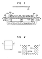
- Fig. 1 shows a sectional view of a planar magnetron sputtering apparatus which is the first embodiment.
- An evacuation system, a radio frequency power source, etc. which are not pertinent to the present invention are not shown.
- the sputtering apparatus has a holey target made of Al 200 and employs a permanent magnet 403 as magnetic field gereration means.
- the permanent magnet 403 generates a magnetic field orthogonal to an electric field which enters perpendicularly to the principal plane of the target 200 and the plane of the bottom 202 of each hole.
- Numeral 401 in the figure designates a substrate to be formed with a film, and numeral 402 an anode.
- argon gas is introduced into the space between the target 200 and the substrate for film formation and 401, l a great minus voltage is applied to the target 200 to induce the glow discharge, and to sputter the target 200, whereby sputtering particles of the target material are formed as the thin film on the substrate for film formation 401.
- Fig. 2 shows the shape of the through-hole of the substrate for film formation (dimensions of the through-hole: 1.5 ⁇ m x 1.5 pm, dimension of a step: 1.5 ⁇ m).
- Fig. 3 shows a result obtained when the through-hole portion shown in Fig. 2 was formed with a film 1 pm thick without employing the holey target according to the present invention.
- the Al film 601 exhibited an the shape of / overhang 602 at the stepped part of the through-hole, and it was hardly formed on the side walls 603 of the through-hole and the bottom 604 thereof.
- Fig. 4 shows a shape obtained when an Al film was formed by 1 ⁇ m by the use of the embodiment shown in Fig. 1.
- the Al film 701 scarcely formed an overhang at the stepped part 702 of the through-hole, and Al films 0.3 ⁇ m and 0.8 ⁇ m thick were respectively formed on the side walls 703 of the through-hole and the bottom 704 thereof.
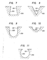
- Figs. 5 thru 11 show modifications of the present embodiment. They illustrate the sectional shapes of holey targets (corresponding to the element 200 in Fig. 1) for use in the present embodiment.
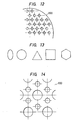
- Fig. 12 shows the arrangement of the holes in the target
- Fig. 13 shows modifications of the shapes of the holes of the target viewed in plan.
- larger and smaller recesses may be combined as illustrated in Fig. 14, or columnar protrusions may be formed on the upper side of the target to equivalently form holes as illustrated in Fig. 15 or Fig. 16.
- the directivity of the sputtering particles which fly and come from the target member is enhanced, and favorable film deposition characteristics free from the overhang shape can be attained.
- a stepped portion corresponding to a through-hole 2 pm in diameter and 2 ⁇ m in depth is formed with a film at a film formation rate of approximately 0.8 ⁇ m/minute, the film is deposited to a thickness of 0.4 ⁇ m on the side walls of the stepped portion, and favorable film deposition characteristics free from an overhang shape can be attained.
- Figs. 17 thru 19 show an embodiment in which a frame is disposed directly in front of a substrate to the end of limiting the incident angle of sputtering particles that enter the substrate for film formation.
- Fig. 18 is a sectional view of a target part and a substrate holder part within the sputtering apparatus
- Fig. 19 is a view of the substrate holder part seen in the direction of an arrow 18 in Fig. 18.
- the sputtering apparatus shown in Figs. 18 and 19 is such that a target 1 which is of y 260 mm and which is made of Al is formed at its peripheral part with a protrusion 14 having a height of 10 mm, and that it is bonded to a backing plate 16.
- electromagnets 15 are arranged on the rear surface of the backing plate 16 and are shaped into a double ring, and applied currents to the respective electromagnets can be changed independently of each other.
- the silicon wafer 2 is set on a substrate holder 17, to which the frame 12 is thereafter fixed by screws 19.
- the frame 12 was so shaped that the height a (Fig. 18) thereof was 19 mm and that the frame width b (Fig.
- the target material was sputtered for 1 minute 25 seconds under the conditions that the gaseous pressure of Al to be sputtered was 3 mTorr, that a voltage applied to the target was 500 - 600 V, that a target current was 12 A, and that the applied currents to the electromagnets 15 were 3 - 6 A for the inner electromagnet (1350 turns) and 8 - 0 A for the outer electromagnet (350 turns).
- the substrate holder 17 was rotated while being moved in paralllel with the plane of the target 1.
- the Al film was formed to a thickness of 1.0 ⁇ m on the upper surface part of the through-hole step and to a thickness of 0.9 pm on the bottom of the through-hole, and an uncovered part on the side surface of the stepped portion did not arise.
- the target material was sputtered for 50 seconds under the same sputtering conditions as mentioned above.
- the deposited Al film was 1.0 pm thick on the top surface of the through-hole step and 0.6 ⁇ m thick on the bottom of the through-hole, the overhang part as shown in Fig. 23 was formed, and uncovered parts appeared on the side surfaces of the step.
- the substrate is depicted on enlarged scale in the thickness direction thereof. More concretely, dimensions in the thickness direction of the substrate are taken in pm, and the other dimensions in mm.
- the uniform film formation can be carried out by disposing the frame according to the present embodiment, but the rate of film formation lowers to some extent. This is ascribable to the fact that, since the particles emitted from the target material are blocked by the frame, the total quantity of sputtering particles to reach the silicon wafer decreases. By properly selecting the configuration of the frame, accordingly, the step coverage can be improved without extremely lowering the film formation rate. Frames may be changed according to the use of the film formation.
- step coverage for a microscopic through-hole portion can be performed without an uncovered part, to bring forth the effect of permitting the formation of a multi-layer interconnection portion of favorable connection reliability in semiconductor devices etc. to be microminiaturized still more.
- Another effect is that a target which has heretofore required an area about four times larger than the area of a substrate can be rendered substantially as small as the substrate, thereby to sharply enhance the utilization factor of the target.
Abstract

Description
- The present invention relates to a planar magnetron sputtering apparatus which forms a thin film by the use of sputtering. More particularly, it relates to a sputtering apparatus of good step coverage by which a substrate to be formed with a film and having a microscopic through-hole or the like as the shape of a stepped part can be formed with the thin film faithfully to the shape.
- A conventional planar magnetron sputtering process is described in detail in, for example, a paper by JHON L. VOSSEN, WERNER KERN et al. contained in "Thin Film Processes", ACADEMIC PRESS, 1978.
- A material to be sputtered is sputtered and scattered by an inert atomic species heavier than a hydrogen atom, such as Ar, thereby to reach a substrate on which a film is to be formed. The directions of the scattering, are controlled according to the cosine law. Therefore, when a stepped part exits on the substrate to be formed with the film, overhangs are formed on the side walls of the step.
- The actual film formation by the sputtering is employed for the production of semiconductor devices (ICs, LSIs, etc.) and various thin-film modules (thermal recording heads, etc.). More concretely, it is important as a technique for forming an interconnection layer, a conductor layer and an insulator layer.
- As described in, for example, a paper "Vacuum Evaporation and Sputtering Apparatus" by Kitabayashi et al. in 'Denshi Zairyo (Electronics Material)', 1981, Separate Volume, pp. 143 - 148, there has been developed an apparatus in which a plasma is confined into the vicinity of a target by an electromagnetic field, thereby to efficiently form a film.
- Besides, in a paper "Planar Magnetron Sputtering Cathode with Deposition rate Distribution Controllability" by Abe et al. in 'Thin Solid Film', Vol. 96 (1982), pp. 225 - 233, a double magnetic pole type electromagnet cathode structure is introduced. Here, it is claimed that a semiconductor substrate of large diameter (1 150 mm) can be formed with a uniform film by operating two electromagnets to control an electromagnetic field distribution and to change an erosion diameter at will.
- Even with the techniques as mentioned above, however, been the microminiaturization of patterns has/attended with the problem that, in a through-hole portion or the like in the case of forming the upper layer of a multilayer interconnection or an object to be formed with a film, already having an interconnection as an under layer, the step coverage becomes insufficient to cause a part where no film is formed. Brief Summary of the Invention:
- An object of the present invention is to provide an apparatus which performs sputtering film formation of favorable step coverage. More in detail, it is to provide a planar magnetron sputtering apparatus in which, in order to form a film on a stepped portion having a microscopic through-hole as per the shape of the underlying step, sputtering particles with a directivity are caused to fly onto a substrate for the film formation, thereby making it possible to form the film faithfully to the shape of the step.
- The present invention is characterized in that inferior film formation coverage attributed to the government of the emission angle distribution of sputtering particles by the cosine law is improved by positively limiting part of the emissive angular extent. That is, the flights of the sputtering particles are physically limi.ted on the side of the emission source of the sputtering particles or/and the side of a substrate to be formed with a film. Brief Description of the Drawings:
- Fig. 1 is a view showing an embodiment of the present invention;
- Fig. 2 is a sectional view showing the step of a substrate for film formation before a film is formed;
- Figs. 3 and 4 are sectional views for explaining steps after films have been formed;
- Figs. 5
thru 11 are views each showing a modification of a recess formed in a recess in a target in Fig. 1; - Fig. 12 is a front view showing the distribution of the recesses formed in the target in Fig. 1;
- Fig. 13 is a view showing modifications of the front shape of the recess formed in the target in Fig.1;
- Fig. 14 is a front view showing another example of the distribution in Fig. 12;
- Fig. 15 shows a front view and a sectional view of pillars which define a configuration equivalent to that of the recesses formed in the target in Fig. 1;
- Fig. 16 shows another modification of the recesses referred to in Fig. 15;
- Fig. 17 is a conceptual view showing another embodiment of the present invention;
- Fig. 18 is a schematic sectional view of the spittering apparatus in Fig. 17;
- Fig. 19 is a schematic plan view of the viciniy of a substrate holder in Fig. 17;
- Fig. 20 is a view for explaining a cycloidal nation;
- Fig. 21 is a view for explaining a magnetron discharge in a target recess;
- Fig. 22 is an explanatory view of the impartation of a directivity to sputtering particles by a holey target; and
- Fig. 23 is a schematic view of a sputtering apparatus in a prior art.
- In order to promote a better understanding of the present invention, the description of the present invention will be started from some ex.planation of the principles of the sputtering technique.
- (A) In a sputtering apparatus, a glow discharge must be maintained within a space of reduced pressure. An electron generated by the discharge performs a helical motion so as to wind round a magnetic field vector /B (Fig. 20). Therefore, the mean free path (hereinbelow, abbreviated to 'mfp') of the electron lengthens. This effect increases the probability of the collision of the electron with the particles of a sputtering gas (usually, the particles of an inert gas such as argon gas); to generate an intense glow discharge. In a hole in a target member shown in Fig. 21, an electron moves to the bottom thereof owing to a magnetron motion based on a magnetic field /B and an electric field /E. This electron performs the magnetron motion also in the bottom portion of the hole. More specifically, when the
electron 101 has approached ahole side wall 201, it is repelled by the electric field of the target at a great minus potential and is pushed back in the direction opposite to that of the magnetron motion. However, the electron is advanced toward thehole side wall 201 by the force of the magnetron motion again, whereupon it is pushed back under the repulsive force of the electric field again. It continues such motions. Therefore, the mfp enlarges, and the intense glow discharge can be sustained even under a pressure of or below 10 3 Torr which is a pressure atmosphere in ordinary sputtering. - Since, in this manner, the glow discharge arises also within the recess provided in the target member, it has become possible to endow the emission directions of the sputtering particles with a directivity by means of the target member provided with the recesses as one embodiment of the present invention.
- More specifically, the discharge concentrates in the hole bottom portion, it concentrates in the hole, and the sputtering phenomenon is induced by the gas ionized plus within the hole. In this regard, the sputtering particles which are emitted according to the ordinary cosine law within the hole have the emission angle distribution thereof limited in accordance with a solid angle defined when a space above the principal surface of the target is viewed from within the hole. Fig. 22 illustrates that the angle of emission of sputtering particles from one point of the hole bottom conforms with the cosine law if side walls are not provided, but that the sputtering particles are blocked by the
hole side walls hole side walls - (B) As already stated, in the case where the stepped portion exists on the substrate to be formed with the film, the inferior step coverage of the stepped portion is attributed to the fact that the entrance of the sputtering particles on the substrate conforms with the cosine law. That is, the sputtering particles entering the substrate perpendicularly are smaller in number than the particles entering the same at any other angles, so that overhangs are formed on the stepped portion to worsen the step coverage.
- Accordingly, it is necessary for the betterment of the step coverage to endow the emission source of sputtering particles with a directivity or to limit the angle of entrance of sputtering particles to enter a substrate for film formation.
- The worsening of the coverage ascribable to the cosine law will be described with reference to Fig. 23.
- In Fig. 23, a target material is sputtered from a sputtering
target 1 to awafer 2. This wafer is previously formed with a first layer ofinterconnection 3, aninter-layer insulator film 4, and through-holes 5 provided in the inter-layer insulator film. The angle of incidence of a sputtering particle on the wafer, with respect to a line perpendicular to the plane of the wafer is denoted by e as indicated in this figure. Here, let's consider the formation of a film on astepped portion 6 defined by the through-holes 5. On theside surface 7 of thestepped portion 6, no particle enters the wafer from a target part lying on the left side of a line which is drawn perpendicularly from a point on theside surface 7 to thetarget 1, so that the number of incident particles on theside surface 7 is naturally smaller than on thetop surface part 8 of the step. Consequently, the amount of film formation on the steptop surface 8 becomes larger, and the particles having incided and deposited on the step top surface as indicated atnumeral 9 in Fig. 23form overhang parts 10. When the overhang parts have been formed, the number of the incident particles on theside surface 7 decreases more. In addition, the size of the through-hole 5 is often set at a value equal to or smaller than the thickness of theinsulator film 4. In such a case, also the number of incident particles on thebottom part 11 of the through-hole decreases on account of the steppedportion 6 and theoverhang parts 10. - These phenomena arise because of the larger amount of film formation based on the incident particles whose angles θ indicated in Fig. 23 are large, and by removing the particles incident at the large angles θ, the betterment of the coverage is achieved as indicated by another embodiment of the present invention. To this end, as shown in Fig. 17, a
frame 12 is disposed in the space between atarget 1 and awafer 2 to remove the incident particles oflarge angles 8. - In Fig. 17, substrate parts (2, 3, 4) are depicted in pm in the thickness direction thereof, and the other parts are depicted in mm. That is, the substrate parts are magnified to 1,000 diameters in the thickness direction as compared with the other parts.
- When the
frame 12 is provided as shown in Fig. 17, there arise the problems of (1) decrease in the rate of film formation on the wafer and (2) lowering in the amount of film formation in apart 13 shaded by the frame. The new problems are solved by contriving (1) a measure wherein a substrate such as the wafer is continuously rotated or moved in parallel, thereby to control a film thickness distribution within the substrate, (2) a measure wherein aprotrusion 14 made of the same material as the target material is provided at the peripheral part of the target, and it is held at the same potential as that of the target, thereby to increase the amount of sputtering on the basis of an increased number of electrons staying near the target, (3) a measure wherein currents which are applied toelectromagnets 15 being magnetic field generation means are changed, thereby to effectively utilize the target material, and so forth. - (C) Now, embodiments of the present invention will be described with reference to the drawings.
- Fig. 1 shows a sectional view of a planar magnetron sputtering apparatus which is the first embodiment. An evacuation system, a radio frequency power source, etc. which are not pertinent to the present invention are not shown. Referring to Fig. 1, the sputtering apparatus has a holey target made of
Al 200 and employs apermanent magnet 403 as magnetic field gereration means. Thepermanent magnet 403 generates a magnetic field orthogonal to an electric field which enters perpendicularly to the principal plane of thetarget 200 and the plane of the bottom 202 of each hole.Numeral 401 in the figure designates a substrate to be formed with a film, and numeral 402 an anode. Using the embodiment shown in Fig. 1, argon gas is introduced into the space between thetarget 200 and the substrate for film formation and 401,la great minus voltage is applied to thetarget 200 to induce the glow discharge, and to sputter thetarget 200, whereby sputtering particles of the target material are formed as the thin film on the substrate forfilm formation 401. - The function and effect of the present embodiment will be described below.
- Fig. 2 shows the shape of the through-hole of the substrate for film formation (dimensions of the through-hole: 1.5 µm x 1.5 pm, dimension of a step: 1.5 µm).
- Fig. 3 shows a result obtained when the through-hole portion shown in Fig. 2 was formed with a
film 1 pm thick without employing the holey target according to the present invention. TheAl film 601 exhibited an the shape of/overhang 602 at the stepped part of the through-hole, and it was hardly formed on theside walls 603 of the through-hole and thebottom 604 thereof. Fig. 4 shows a shape obtained when an Al film was formed by 1 µm by the use of the embodiment shown in Fig. 1. In this case, theAl film 701 scarcely formed an overhang at the steppedpart 702 of the through-hole, and Al films 0.3 µm and 0.8 µm thick were respectively formed on theside walls 703 of the through-hole and thebottom 704 thereof. - Figs. 5 thru 11 show modifications of the present embodiment. They illustrate the sectional shapes of holey targets (corresponding to the
element 200 in Fig. 1) for use in the present embodiment. - Fig. 12 shows the arrangement of the holes in the target, while Fig. 13 shows modifications of the shapes of the holes of the target viewed in plan. In order to increase the area of the recesses in the target, larger and smaller recesses may be combined as illustrated in Fig. 14, or columnar protrusions may be formed on the upper side of the target to equivalently form holes as illustrated in Fig. 15 or Fig. 16.
- According to the present embodiment, the directivity of the sputtering particles which fly and come from the target member is enhanced, and favorable film deposition characteristics free from the overhang shape can be attained.
- By way of example, when a stepped portion corresponding to a through-
hole 2 pm in diameter and 2 µm in depth is formed with a film at a film formation rate of approximately 0.8 µm/minute, the film is deposited to a thickness of 0.4 µm on the side walls of the stepped portion, and favorable film deposition characteristics free from an overhang shape can be attained. - Figs. 17 thru 19 show an embodiment in which a frame is disposed directly in front of a substrate to the end of limiting the incident angle of sputtering particles that enter the substrate for film formation.
- Let's exemplify a case where an
Al film 1 µm thick as a first layer of interconnection and apolyimide film 2 pm thick as an inter-layer insulator film are successively formed on a silicon wafer of φ 100 mm (100 mm in diameter) and where through-holes ofφ 2 um are formed in the polyimide resin. The resulting wafer is set in the sputtering apparatus of the present embodiment illustrated in Figs. 18 and 19. In this case, Fig. 18 is a sectional view of a target part and a substrate holder part within the sputtering apparatus, while Fig. 19 is a view of the substrate holder part seen in the direction of an arrow 18 in Fig. 18. The sputtering apparatus shown in Figs. 18 and 19 is such that atarget 1 which is of y 260 mm and which is made of Al is formed at its peripheral part with aprotrusion 14 having a height of 10 mm, and that it is bonded to abacking plate 16. Besides,electromagnets 15 are arranged on the rear surface of thebacking plate 16 and are shaped into a double ring, and applied currents to the respective electromagnets can be changed independently of each other. In addition, thesilicon wafer 2 is set on a substrate holder 17, to which theframe 12 is thereafter fixed byscrews 19. By way of example, theframe 12 was so shaped that the height a (Fig. 18) thereof was 19 mm and that the frame width b (Fig. 19) thereof was 0.5 mm, and each subdivision defined by the frame was in the shape of a regular square one side c (Fig. 19) of which was 19.5 mm. The distance between the wafer and the plane of the target was 80 mm. With this sputtering apparatus, the target material was sputtered for 1 minute 25 seconds under the conditions that the gaseous pressure of Al to be sputtered was 3 mTorr, that a voltage applied to the target was 500 - 600 V, that a target current was 12 A, and that the applied currents to theelectromagnets 15 were 3 - 6 A for the inner electromagnet (1350 turns) and 8 - 0 A for the outer electromagnet (350 turns). During the sputtering, the substrate holder 17 was rotated while being moved in paralllel with the plane of thetarget 1. As a result, the Al film was formed to a thickness of 1.0 µm on the upper surface part of the through-hole step and to a thickness of 0.9 pm on the bottom of the through-hole, and an uncovered part on the side surface of the stepped portion did not arise. For the sake of comparison, using the prior-art sputtering apparatus which was not furnished with theframe 12 and theprotrusion 14 of the target, the target material was sputtered for 50 seconds under the same sputtering conditions as mentioned above. As a result, the deposited Al film was 1.0 pm thick on the top surface of the through-hole step and 0.6 µm thick on the bottom of the through-hole, the overhang part as shown in Fig. 23 was formed, and uncovered parts appeared on the side surfaces of the step. - In Fig. 23, the substrate is depicted on enlarged scale in the thickness direction thereof. More concretely, dimensions in the thickness direction of the substrate are taken in pm, and the other dimensions in mm.
- It is understood that the uniform film formation can be carried out by disposing the frame according to the present embodiment, but the rate of film formation lowers to some extent. This is ascribable to the fact that, since the particles emitted from the target material are blocked by the frame, the total quantity of sputtering particles to reach the silicon wafer decreases. By properly selecting the configuration of the frame, accordingly, the step coverage can be improved without extremely lowering the film formation rate. Frames may be changed according to the use of the film formation.
- According to the present embodiment, step coverage for a microscopic through-hole portion can be performed without an uncovered part, to bring forth the effect of permitting the formation of a multi-layer interconnection portion of favorable connection reliability in semiconductor devices etc. to be microminiaturized still more. Another effect is that a target which has heretofore required an area about four times larger than the area of a substrate can be rendered substantially as small as the substrate, thereby to sharply enhance the utilization factor of the target.
Claims (4)
Applications Claiming Priority (4)
| Application Number | Priority Date | Filing Date | Title |
|---|---|---|---|
| JP23835484A JPH0660390B2 (en) | 1984-11-14 | 1984-11-14 | Planar magnetron method and apparatus for forming a film on a film formation target substrate having micropores |
| JP59238358A JPS61117276A (en) | 1984-11-14 | 1984-11-14 | Target for sputtering |
| JP238358/84 | 1984-11-14 | ||
| JP238354/84 | 1984-11-14 |
Publications (3)
| Publication Number | Publication Date |
|---|---|
| EP0187226A2 true EP0187226A2 (en) | 1986-07-16 |
| EP0187226A3 EP0187226A3 (en) | 1987-04-08 |
| EP0187226B1 EP0187226B1 (en) | 1990-01-31 |
Family
ID=26533654
Family Applications (1)
| Application Number | Title | Priority Date | Filing Date |
|---|---|---|---|
| EP85114424A Expired - Lifetime EP0187226B1 (en) | 1984-11-14 | 1985-11-13 | Sputtering apparatus with film forming directivity |
Country Status (4)
| Country | Link |
|---|---|
| US (1) | US4724060A (en) |
| EP (1) | EP0187226B1 (en) |
| KR (1) | KR900001825B1 (en) |
| DE (1) | DE3575811D1 (en) |
Cited By (4)
| Publication number | Priority date | Publication date | Assignee | Title |
|---|---|---|---|---|
| EP0628986A1 (en) * | 1993-06-11 | 1994-12-14 | Applied Materials, Inc. | Self cleaning collimator |
| EP0634779A1 (en) * | 1993-06-11 | 1995-01-18 | Applied Materials, Inc. | Collimation chamber with rotatable pedestal |
| GB2315781A (en) * | 1996-07-30 | 1998-02-11 | Nec Corp | Sputtering target with collimating holes |
| DE19819933A1 (en) * | 1998-05-05 | 1999-11-11 | Leybold Systems Gmbh | Target for a cathode sputtering device for producing thin layers |
Families Citing this family (56)
| Publication number | Priority date | Publication date | Assignee | Title |
|---|---|---|---|---|
| US4824544A (en) * | 1987-10-29 | 1989-04-25 | International Business Machines Corporation | Large area cathode lift-off sputter deposition device |
| US5015331A (en) * | 1988-08-30 | 1991-05-14 | Matrix Integrated Systems | Method of plasma etching with parallel plate reactor having a grid |
| US5133849A (en) * | 1988-12-12 | 1992-07-28 | Ricoh Company, Ltd. | Thin film forming apparatus |
| US4957605A (en) * | 1989-04-17 | 1990-09-18 | Materials Research Corporation | Method and apparatus for sputter coating stepped wafers |
| US5635036A (en) * | 1990-01-26 | 1997-06-03 | Varian Associates, Inc. | Collimated deposition apparatus and method |
| US6521106B1 (en) * | 1990-01-29 | 2003-02-18 | Novellus Systems, Inc. | Collimated deposition apparatus |
| EP0440377B1 (en) * | 1990-01-29 | 1998-03-18 | Varian Associates, Inc. | Collimated deposition apparatus and method |
| US5437778A (en) * | 1990-07-10 | 1995-08-01 | Telic Technologies Corporation | Slotted cylindrical hollow cathode/magnetron sputtering device |
| AU8629491A (en) * | 1990-08-30 | 1992-03-30 | Materials Research Corporation | Pretextured cathode sputtering target and method of preparation thereof and sputtering therewith |
| JP2725944B2 (en) * | 1991-04-19 | 1998-03-11 | インターナショナル・ビジネス・マシーンズ・コーポレイション | Metal layer deposition method |
| CA2061119C (en) * | 1991-04-19 | 1998-02-03 | Pei-Ing P. Lee | Method of depositing conductors in high aspect ratio apertures |
| JPH05160070A (en) * | 1991-05-31 | 1993-06-25 | Texas Instr Inc <Ti> | Contact of semiconductor device and manufacture thereof |
| US5171412A (en) * | 1991-08-23 | 1992-12-15 | Applied Materials, Inc. | Material deposition method for integrated circuit manufacturing |
| US5334302A (en) * | 1991-11-15 | 1994-08-02 | Tokyo Electron Limited | Magnetron sputtering apparatus and sputtering gun for use in the same |
| US5223108A (en) * | 1991-12-30 | 1993-06-29 | Materials Research Corporation | Extended lifetime collimator |
| US5300813A (en) * | 1992-02-26 | 1994-04-05 | International Business Machines Corporation | Refractory metal capped low resistivity metal conductor lines and vias |
| US5371042A (en) * | 1992-06-16 | 1994-12-06 | Applied Materials, Inc. | Method of filling contacts in semiconductor devices |
| US5367412A (en) * | 1992-09-10 | 1994-11-22 | Rohm Co., Ltd. | Recording/reproducing circuit and recording/reproducing apparatus having the same circuit |
| JP3169151B2 (en) * | 1992-10-26 | 2001-05-21 | 三菱電機株式会社 | Thin film forming equipment |
| US5384281A (en) * | 1992-12-29 | 1995-01-24 | International Business Machines Corporation | Non-conformal and oxidizable etch stops for submicron features |
| US5378660A (en) * | 1993-02-12 | 1995-01-03 | Applied Materials, Inc. | Barrier layers and aluminum contacts |
| US5358616A (en) * | 1993-02-17 | 1994-10-25 | Ward Michael G | Filling of vias and contacts employing an aluminum-germanium alloy |
| US5415753A (en) * | 1993-07-22 | 1995-05-16 | Materials Research Corporation | Stationary aperture plate for reactive sputter deposition |
| US5409587A (en) * | 1993-09-16 | 1995-04-25 | Micron Technology, Inc. | Sputtering with collinator cleaning within the sputtering chamber |
| US5472565A (en) * | 1993-11-17 | 1995-12-05 | Lam Research Corporation | Topology induced plasma enhancement for etched uniformity improvement |
| US5958193A (en) * | 1994-02-01 | 1999-09-28 | Vlsi Technology, Inc. | Sputter deposition with mobile collimator |
| TW278206B (en) * | 1994-03-28 | 1996-06-11 | Materials Research Corp | |
| US5711858A (en) * | 1994-04-12 | 1998-01-27 | International Business Machines Corporation | Process for depositing a conductive thin film upon an integrated circuit substrate |
| US5527438A (en) * | 1994-12-16 | 1996-06-18 | Applied Materials, Inc. | Cylindrical sputtering shield |
| US5982986A (en) | 1995-02-03 | 1999-11-09 | Applied Materials, Inc. | Apparatus and method for rotationally aligning and degassing semiconductor substrate within single vacuum chamber |
| US5885425A (en) * | 1995-06-06 | 1999-03-23 | International Business Machines Corporation | Method for selective material deposition on one side of raised or recessed features |
| US5757879A (en) * | 1995-06-07 | 1998-05-26 | International Business Machines Corporation | Tungsten absorber for x-ray mask |
| US5725739A (en) * | 1996-07-08 | 1998-03-10 | Micron Technology, Inc. | Low angle, low energy physical vapor deposition of alloys |
| US5783282A (en) | 1996-10-07 | 1998-07-21 | Micron Technology, Inc. | Resputtering to achieve better step coverage of contact holes |
| US6162297A (en) * | 1997-09-05 | 2000-12-19 | Applied Materials, Inc. | Embossed semiconductor fabrication parts |
| US6140236A (en) * | 1998-04-21 | 2000-10-31 | Kabushiki Kaisha Toshiba | High throughput A1-Cu thin film sputtering process on small contact via for manufacturable beol wiring |
| US6592728B1 (en) * | 1998-08-04 | 2003-07-15 | Veeco-Cvc, Inc. | Dual collimated deposition apparatus and method of use |
| US6933508B2 (en) | 2002-03-13 | 2005-08-23 | Applied Materials, Inc. | Method of surface texturizing |
| US6812471B2 (en) * | 2002-03-13 | 2004-11-02 | Applied Materials, Inc. | Method of surface texturizing |
| US20060032740A1 (en) * | 2004-08-16 | 2006-02-16 | Williams Advanced Materials, Inc. | Slotted thin-film sputter deposition targets for ferromagnetic materials |
| TWI265202B (en) * | 2005-03-02 | 2006-11-01 | Asia Optical Co Inc | Tool and device for dedicate coating a photochemical film on a substrate |
| US20060292310A1 (en) * | 2005-06-27 | 2006-12-28 | Applied Materials, Inc. | Process kit design to reduce particle generation |
| JP4923450B2 (en) * | 2005-07-01 | 2012-04-25 | 富士ゼロックス株式会社 | Batch processing support apparatus and method, program |
| US20070012558A1 (en) * | 2005-07-13 | 2007-01-18 | Applied Materials, Inc. | Magnetron sputtering system for large-area substrates |
| US20070012663A1 (en) * | 2005-07-13 | 2007-01-18 | Akihiro Hosokawa | Magnetron sputtering system for large-area substrates having removable anodes |
| US20070084720A1 (en) * | 2005-07-13 | 2007-04-19 | Akihiro Hosokawa | Magnetron sputtering system for large-area substrates having removable anodes |
| US20070012559A1 (en) * | 2005-07-13 | 2007-01-18 | Applied Materials, Inc. | Method of improving magnetron sputtering of large-area substrates using a removable anode |
| US20070051616A1 (en) * | 2005-09-07 | 2007-03-08 | Le Hienminh H | Multizone magnetron assembly |
| US20070056843A1 (en) * | 2005-09-13 | 2007-03-15 | Applied Materials, Inc. | Method of processing a substrate using a large-area magnetron sputtering chamber with individually controlled sputtering zones |
| US20070056850A1 (en) * | 2005-09-13 | 2007-03-15 | Applied Materials, Inc. | Large-area magnetron sputtering chamber with individually controlled sputtering zones |
| US7588668B2 (en) | 2005-09-13 | 2009-09-15 | Applied Materials, Inc. | Thermally conductive dielectric bonding of sputtering targets using diamond powder filler or thermally conductive ceramic fillers |
| US20090166183A1 (en) * | 2007-12-28 | 2009-07-02 | Yinshi Liu | Method of manufacturing a perpendicular magnetic write head with stepped trailing magnetic shield using collimated sputter deposition |
| US20090194414A1 (en) * | 2008-01-31 | 2009-08-06 | Nolander Ira G | Modified sputtering target and deposition components, methods of production and uses thereof |
| KR101611410B1 (en) * | 2009-04-07 | 2016-04-11 | 삼성전자주식회사 | Manufacturing method of graphene |
| US20200135464A1 (en) * | 2018-10-30 | 2020-04-30 | Applied Materials, Inc. | Methods and apparatus for patterning substrates using asymmetric physical vapor deposition |
| DE102021104255A1 (en) * | 2021-02-23 | 2022-08-25 | Cemecon Ag. | sputtering target |
Citations (3)
| Publication number | Priority date | Publication date | Assignee | Title |
|---|---|---|---|---|
| US4401546A (en) * | 1981-03-27 | 1983-08-30 | Nihon Shinku Gijutsu Kabushiki Kaisha | Ferromagnetic high speed sputtering apparatus |
| EP0144572A2 (en) * | 1983-12-05 | 1985-06-19 | Leybold Aktiengesellschaft | Magnetron-cathodes for the sputtering of ferromagnetic targets |
| EP0154859A1 (en) * | 1984-03-07 | 1985-09-18 | International Business Machines Corporation | Apparatus for vacuum deposition |
Family Cites Families (10)
| Publication number | Priority date | Publication date | Assignee | Title |
|---|---|---|---|---|
| US4170541A (en) * | 1978-08-14 | 1979-10-09 | Varian Associates, Inc. | Rotating resonator for large substrate tables in sputtering systems |
| US4322277A (en) * | 1980-11-17 | 1982-03-30 | Rca Corporation | Step mask for substrate sputtering |
| US4391034A (en) * | 1980-12-22 | 1983-07-05 | Ibm Corporation | Thermally compensated shadow mask |
| DE3112104A1 (en) * | 1981-03-27 | 1982-10-07 | Leybold-Heraeus GmbH, 5000 Köln | METHOD AND DEVICE FOR PRODUCING ELECTRICALLY CONDUCTIVE TRANSPARENT OXIDE LAYERS |
| US4410407A (en) * | 1981-12-22 | 1983-10-18 | Raytheon Company | Sputtering apparatus and methods |
| US4474659A (en) * | 1982-05-28 | 1984-10-02 | Fazal Fazlin | Plated-through-hole method |
| DE3223245C2 (en) * | 1982-07-23 | 1986-05-22 | Nihon Shinku Gijutsu K.K., Chigasaki, Kanagawa | High speed ferromagnetic sputtering device |
| US4414086A (en) * | 1982-11-05 | 1983-11-08 | Varian Associates, Inc. | Magnetic targets for use in sputter coating apparatus |
| US4414087A (en) * | 1983-01-31 | 1983-11-08 | Meckel Benjamin B | Magnetically-assisted sputtering method for producing vertical recording media |
| JPS59207631A (en) * | 1983-05-11 | 1984-11-24 | Semiconductor Res Found | Dry process employing photochemistry |
-
1985
- 1985-11-12 KR KR1019850008419A patent/KR900001825B1/en not_active IP Right Cessation
- 1985-11-13 EP EP85114424A patent/EP0187226B1/en not_active Expired - Lifetime
- 1985-11-13 DE DE8585114424T patent/DE3575811D1/en not_active Expired - Lifetime
- 1985-11-14 US US06/797,966 patent/US4724060A/en not_active Expired - Fee Related
Patent Citations (3)
| Publication number | Priority date | Publication date | Assignee | Title |
|---|---|---|---|---|
| US4401546A (en) * | 1981-03-27 | 1983-08-30 | Nihon Shinku Gijutsu Kabushiki Kaisha | Ferromagnetic high speed sputtering apparatus |
| EP0144572A2 (en) * | 1983-12-05 | 1985-06-19 | Leybold Aktiengesellschaft | Magnetron-cathodes for the sputtering of ferromagnetic targets |
| EP0154859A1 (en) * | 1984-03-07 | 1985-09-18 | International Business Machines Corporation | Apparatus for vacuum deposition |
Non-Patent Citations (2)
| Title |
|---|
| IBM TECHNICAL DISCLOSURE BULLETIN, vol. 20, no. 2, July 1977, page 756, New York, US; T.N. KENNEDY: "Chevron sputtering catcher" * |
| JOURNAL OF PHYSICS E, SCIENTIFIC INSTRUMENTS, vol. 12, no. 3, March 1979, pages 159-167, The Institute of Physics, London, GB; J.L. VOSSEN: "The preparation of substrates for film deposition using glow discharge techniques" * |
Cited By (4)
| Publication number | Priority date | Publication date | Assignee | Title |
|---|---|---|---|---|
| EP0628986A1 (en) * | 1993-06-11 | 1994-12-14 | Applied Materials, Inc. | Self cleaning collimator |
| EP0634779A1 (en) * | 1993-06-11 | 1995-01-18 | Applied Materials, Inc. | Collimation chamber with rotatable pedestal |
| GB2315781A (en) * | 1996-07-30 | 1998-02-11 | Nec Corp | Sputtering target with collimating holes |
| DE19819933A1 (en) * | 1998-05-05 | 1999-11-11 | Leybold Systems Gmbh | Target for a cathode sputtering device for producing thin layers |
Also Published As
| Publication number | Publication date |
|---|---|
| KR860004163A (en) | 1986-06-18 |
| KR900001825B1 (en) | 1990-03-24 |
| DE3575811D1 (en) | 1990-03-08 |
| EP0187226B1 (en) | 1990-01-31 |
| EP0187226A3 (en) | 1987-04-08 |
| US4724060A (en) | 1988-02-09 |
Similar Documents
| Publication | Publication Date | Title |
|---|---|---|
| EP0187226A2 (en) | Sputtering apparatus with film forming directivity | |
| US4508612A (en) | Shield for improved magnetron sputter deposition into surface recesses | |
| EP0148504B2 (en) | Method and apparatus for sputtering | |
| KR100302818B1 (en) | Physical Vapor Deposition Using Ion Extraction from Plasma | |
| US4925542A (en) | Plasma plating apparatus and method | |
| US4911814A (en) | Thin film forming apparatus and ion source utilizing sputtering with microwave plasma | |
| US4574179A (en) | Ion beam machining device | |
| JPH1174225A (en) | Sustained self-sputtering reactor having increased density plasma | |
| US3669860A (en) | Method and apparatus for applying a film to a substrate surface by diode sputtering | |
| EP0523695B1 (en) | A sputtering apparatus and an ion source | |
| JPH0660391B2 (en) | Sputtering equipment | |
| JP2000331995A (en) | Flat plate gas introduction device of ccp reaction vessel | |
| US5133849A (en) | Thin film forming apparatus | |
| JPS61221363A (en) | Sputtering apparatus | |
| JP2781165B2 (en) | Sputtering equipment | |
| JPH01139762A (en) | Sputtering apparatus | |
| JPH0867981A (en) | Sputtering device | |
| JPS60194071A (en) | Method and device for forming thin film | |
| JPS637366A (en) | Magnetron sputtering device | |
| JPH0660390B2 (en) | Planar magnetron method and apparatus for forming a film on a film formation target substrate having micropores | |
| JPH01240648A (en) | Thin multicomponent-system film forming equipment | |
| JPH05179438A (en) | Sputtering device | |
| JPH0586476B2 (en) | ||
| JPH09228042A (en) | Thin film forming device and formation of thin film | |
| JPS62174375A (en) | Thin film deposition device |
Legal Events
| Date | Code | Title | Description |
|---|---|---|---|
| PUAI | Public reference made under article 153(3) epc to a published international application that has entered the european phase |
Free format text: ORIGINAL CODE: 0009012 |
|
| AK | Designated contracting states |
Kind code of ref document: A2 Designated state(s): DE FR NL |
|
| PUAL | Search report despatched |
Free format text: ORIGINAL CODE: 0009013 |
|
| AK | Designated contracting states |
Kind code of ref document: A3 Designated state(s): DE FR NL |
|
| 17P | Request for examination filed |
Effective date: 19870410 |
|
| 17Q | First examination report despatched |
Effective date: 19880607 |
|
| GRAA | (expected) grant |
Free format text: ORIGINAL CODE: 0009210 |
|
| STAA | Information on the status of an ep patent application or granted ep patent |
Free format text: STATUS: THE PATENT HAS BEEN GRANTED |
|
| AK | Designated contracting states |
Kind code of ref document: B1 Designated state(s): DE FR NL |
|
| REF | Corresponds to: |
Ref document number: 3575811 Country of ref document: DE Date of ref document: 19900308 |
|
| ET | Fr: translation filed | ||
| PLBE | No opposition filed within time limit |
Free format text: ORIGINAL CODE: 0009261 |
|
| 26N | No opposition filed | ||
| PGFP | Annual fee paid to national office [announced via postgrant information from national office to epo] |
Ref country code: FR Payment date: 19921119 Year of fee payment: 8 |
|
| PGFP | Annual fee paid to national office [announced via postgrant information from national office to epo] |
Ref country code: NL Payment date: 19921130 Year of fee payment: 8 |
|
| PGFP | Annual fee paid to national office [announced via postgrant information from national office to epo] |
Ref country code: DE Payment date: 19930126 Year of fee payment: 8 |
|
| PG25 | Lapsed in a contracting state [announced via postgrant information from national office to epo] |
Ref country code: NL Effective date: 19940601 |
|
| NLV4 | Nl: lapsed or anulled due to non-payment of the annual fee | ||
| PG25 | Lapsed in a contracting state [announced via postgrant information from national office to epo] |
Ref country code: FR Effective date: 19940729 |
|
| PG25 | Lapsed in a contracting state [announced via postgrant information from national office to epo] |
Ref country code: DE Effective date: 19940802 |
|
| REG | Reference to a national code |
Ref country code: FR Ref legal event code: ST |