EP0148504B2 - Method and apparatus for sputtering - Google Patents
Method and apparatus for sputtering Download PDFInfo
- Publication number
- EP0148504B2 EP0148504B2 EP84116391A EP84116391A EP0148504B2 EP 0148504 B2 EP0148504 B2 EP 0148504B2 EP 84116391 A EP84116391 A EP 84116391A EP 84116391 A EP84116391 A EP 84116391A EP 0148504 B2 EP0148504 B2 EP 0148504B2
- Authority
- EP
- European Patent Office
- Prior art keywords
- target
- magnetic field
- plasma
- substrate
- sputtering
- Prior art date
- Legal status (The legal status is an assumption and is not a legal conclusion. Google has not performed a legal analysis and makes no representation as to the accuracy of the status listed.)
- Expired - Lifetime
Links
Images


Classifications
-
- H—ELECTRICITY
- H01—ELECTRIC ELEMENTS
- H01J—ELECTRIC DISCHARGE TUBES OR DISCHARGE LAMPS
- H01J37/00—Discharge tubes with provision for introducing objects or material to be exposed to the discharge, e.g. for the purpose of examination or processing thereof
- H01J37/32—Gas-filled discharge tubes
- H01J37/32009—Arrangements for generation of plasma specially adapted for examination or treatment of objects, e.g. plasma sources
- H01J37/32192—Microwave generated discharge
-
- C—CHEMISTRY; METALLURGY
- C23—COATING METALLIC MATERIAL; COATING MATERIAL WITH METALLIC MATERIAL; CHEMICAL SURFACE TREATMENT; DIFFUSION TREATMENT OF METALLIC MATERIAL; COATING BY VACUUM EVAPORATION, BY SPUTTERING, BY ION IMPLANTATION OR BY CHEMICAL VAPOUR DEPOSITION, IN GENERAL; INHIBITING CORROSION OF METALLIC MATERIAL OR INCRUSTATION IN GENERAL
- C23C—COATING METALLIC MATERIAL; COATING MATERIAL WITH METALLIC MATERIAL; SURFACE TREATMENT OF METALLIC MATERIAL BY DIFFUSION INTO THE SURFACE, BY CHEMICAL CONVERSION OR SUBSTITUTION; COATING BY VACUUM EVAPORATION, BY SPUTTERING, BY ION IMPLANTATION OR BY CHEMICAL VAPOUR DEPOSITION, IN GENERAL
- C23C14/00—Coating by vacuum evaporation, by sputtering or by ion implantation of the coating forming material
- C23C14/22—Coating by vacuum evaporation, by sputtering or by ion implantation of the coating forming material characterised by the process of coating
- C23C14/34—Sputtering
- C23C14/46—Sputtering by ion beam produced by an external ion source
-
- H—ELECTRICITY
- H01—ELECTRIC ELEMENTS
- H01J—ELECTRIC DISCHARGE TUBES OR DISCHARGE LAMPS
- H01J37/00—Discharge tubes with provision for introducing objects or material to be exposed to the discharge, e.g. for the purpose of examination or processing thereof
- H01J37/32—Gas-filled discharge tubes
- H01J37/32431—Constructional details of the reactor
- H01J37/3266—Magnetic control means
-
- H—ELECTRICITY
- H01—ELECTRIC ELEMENTS
- H01J—ELECTRIC DISCHARGE TUBES OR DISCHARGE LAMPS
- H01J37/00—Discharge tubes with provision for introducing objects or material to be exposed to the discharge, e.g. for the purpose of examination or processing thereof
- H01J37/32—Gas-filled discharge tubes
- H01J37/34—Gas-filled discharge tubes operating with cathodic sputtering
Definitions
- This invention relates to sputtering, and more particularly to the so-called plasma sputtering according to which cations existing in plasma are accelerated by an electric field to impinge against the surface of a target thereby depositing the material of the target on the surface of a substrate or a workpiece.
- Sputtering is one of important techniques used for film deposition, e.g. in the course of manufacture of semiconductor devices.
- the process of sputtering includes generally ionizing an inert gas (for example, argon) to generate cations and accelerating the cations to impinge against the surface of a target, thereby causing emission of constituent atoms or molecules from the target and depositing the liberated atoms or molecules on the surface of a substrate disposed opposite to the target.
- the deposition rate or speed is dependent upon the number of ions incident on the surface of the target and the sputtering yield of the ions. It is effective to utilize plasma at a high density for increasing the number of incident ions.
- Planar magnetron sputtering is known in which a target is disposed on or above a cathode, and a central magnetic pole member and a peripheral magnetic pole member are disposed in the cathode disposed underneath the target. There is formed a closed loop of magnetic field in the electrode structure. Due to the above arrangement, arcuate lines of magnetic force extending through the target in the thicknesswise direction thereof appear between the central magnetic pole member and the peripheral magnetic pole member. These magnetic lines of force flow in the radial direction when viewed from the upside of the target. The central portion of the magnetic lines of force forms an upward convex arc on the surface of the target.
- the profile of the magnetic lines of force on the target is analogous to that of a doughnut truncated in its lower portion.
- Plasma is produced when the electric field is built up by the electrode structure in the presence of a low-pressure gas introduced into such a magnetic field, and electrons tending to migrate outward from the doughnut-like portion are deflected by the magnetic field to be confined within the extent of the magnetic field distribution. These electrons contribute to further ionization of the gas molecules.
- high-density plasma in the form of a doughnut (toroidal ring) or a hollow circle (loop) is produced on the target.
- Cations (inert gas ions) in the plasma are accelerated toward the target by the electric field to effect sputtering. As a result, the corresponding area of the target is eroded in the form of a hollow ring or loop.
- the target is eroded in its local area only. Therefore, the ratio of the sputtering-participating area to the entire area of the surface of the target (the target utilization efficiency) is low, the deposition rate is low, and the useful service life of the target is short.
- a proposal for changing the diameter of the magnetic flux distribution thereby widening the eroded surface area of the target has been made, as disclosed, for example, in USP 4,401,539 assigned to the present assignee. According to the proposal, however, only a limited portion of the surface area of the target is utilized for sputtering at a moment. It has therefore been strongly demanded to develop a method and apparatus which can more effectively utilize the target so that the entire surface area of the target can serve as a source of vaporization or sputtering.
- FR-A-2,324,755 discloses an apparatus and a method of sputtering in which a magnetic field is applied parallel to a surface above which the plasma is confined.
- DE-A-3,144,016 discloses a plasma processing apparatus where a plasma stream produced by microwave is transferred using magnetic means.
- JP-A-58-75839 there is disclosed a sputtering apparatus for forming a high-density torus plasma on a target by a magnetic field in which microwave is introduced in the vicinity of a gas inlet of a processing chamber so as to increase the plasma density and the processing rate.
- the inventors contemplate to generate a magnetic field of such a configuration which does not substantially include magnetic lines of force traversing a target and forming closed loops in an electrode structure, so that high-density plasma can be produced in the magnetic field of the above configuration for the purpose of effecting efficient sputtering.
- the combination of a mirror magnetic field and a source of microwave is used to produce high-density plasma thereby efficiently sputtering the material of a target on the surface of a substrate.
- the mirror magnetic field can be produced by a pair of magnets.
- the high-density plasma can thus be maintained above the target over a wide surface area of the target.
- the optimized sputtering conditions can be selected as desired to meet the material of the target.
- the capability of attaining desired sputtering of material over the wide surface area of the target can greatly increase the rate of film deposition by sputtering and can also greatly improve the rate of utilization of the target.
- the capability of selecting the optimized sputtering conditions meeting the material of the target improves the efficiency of production and also improves the rate of utilization of material as well as the performance of semiconductor devices.
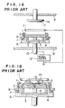
- Figs. 1A and 1B show schematically the structure of a prior art, planar magnetron sputtering apparatus.
- a target plate (referred to hereinafter merely as a target) 1 is backed up at its rear surface by a backing plate 2.
- a peripheral annular magnetic pole member 4 and a central solid cylindrical magnetic pole member 5 Disposed on the rear surface side of the backing plate 2 are a peripheral annular magnetic pole member 4 and a central solid cylindrical magnetic pole member 5 which are magnetically coupled to each other by a yoke 3 to constitute a magnetic circuit.
- the target 1 and the backing plate 2 are made of non-magnetic materials respectively, and the lines of magnetic flux flowing between the magnetic members draw an arc extending through the target 1 in the thicknesswise direction of the target 1 as shown in Fig. 1B.
- a cathode 6 encloses the magnetic members 4, 5 and yoke 3 therein and is hermetically closed by the backing plate 2.
- a shield 8 is mounted on the outer peripheral portion of the cathode 6 with an annular insulating member 7 interposed therebetween.
- the cathode 6 is supported on a shaft 10 which is electrically insulated from and hermetically secured to a hermetic or vacuum enclosure wall 9 of a vacuum chamber.
- An anode 11 is disposed above the cathode 6, and a power source 12 is connected between the anode 11 and the cathode 6.
- the lines of magnetic force in the vicinity of the surface of the target 1 are distributed to provide a doughnut-like or semi-annular magnetic field distribution 13 as best seen in Fig. 1B.
- Application of the power supply voltage across the anode 11 and the cathode 6 generates plasma.
- the semi-annular magnetic field distribution 13 acts to confine the plasma so that the plasma has a high density in a toroidal ring region 14 shown in Fig. 1B.
- the ions in the plasma are accelerated by an electric field substantially perpendicular to the surface of the target 1 to impinge against the surface of the target 1.
- the constituent atoms or particles are sputtered out from the surface of the target 1 to leave a locally eroded or etched region 15 on the target surface.
- the atoms or particles sputtered out from the surface of the target 1 migrate toward and onto the lower surface of a substrate 17 supported on a substrate stage 16 to deposit and form a thin film on the lower surface of the substrate 17.
- the eroded or etched region 15 on the surface of the target 1 is progressively widened with time due to repetition of the sputtering process.
- this erosion is generally limited to a specific region on the surface of the target 1 in the target arrangement shown in Fig. 1B.
- the plasma has a high density above a limited region only of the surface of the target 1, and progressive erosion of the target 1 due to repeated sputtering is limited to a specific region only of the target 1. Because of the limited small area of the source of sputtering, the rate of deposition of the target material on the substrate 17 cannot be increased, and the rate of utilization of the target surface is also low.
- the present invention eliminates the use of the magnets disposed beneath the target in the electrode structure of the prior art magnetron sputtering apparatus and yet attains the formation of high-density plasma over a wide area of the surface of the target. More precisely, according to the present invention, high-density plasma covering a substantial area of the surface of the target is generated without resorting to the use of a magnetic field forming a closed loop of magnetic flux extending through the target in the thicknesswise direction of the target.
- Plasma having a high density is generated with the use of a magnetic field not forming a closed loop inside the electrode structure which contains the target, unlike the prior art, and the plasma is maintained above the target to cover a wide area of the surface of the target for effecting desired sputtering.
- magnets for establishing a mirror magnetic field are disposed at a place remote from a target, and microwaves are introduced toward and into the space defined by the lines of magnetic force of the mirror magnetic field thereby generating plasma having a high density.
- the space defined by the magnetic lines of force of the mirror magnetic field (the intermediate bulged portion of the magnetic flux) exhibits a confinement effect on the plasma.
- the electrode structure in the present invention includes an anode and a cathode (a power source is to be connected therebetween), and a target is supported on the cathode. Therefore, an electric field substantially perpendicular to the surface of the target is produced. Cations existing above the target are accelerated by the electric field to impinge against the target.
- the absence of any magnetic lines of force forming a closed loop in the electrode structure which contains the target is equivalent to or indicates the absence of a magnetic flux distribution drawing an arc above the target and having a bulged portion extending adjacent to a limited region only of the target. Therefore, a limited region only of the target is not eroded unlike that employed in the prior art sputtering apparatus of the planar magnetron type.
- the high-density plasma is generated by the aid of the mirror magnetic field, but the plasma is not localized to a limited region only of the target.
- the high-density plasma is maintained in an area above the target according to, for example, one of the following manners: (1) The high-density plasma is generated at a place distant from the target by the combination of a mirror magnetic field and microwaves, and the thus generated high-density plasma is guided to migrate toward an area above the target. (2) Plasma migrated according to the method (1) is confined in a magnetic field whose lines of force do not penetrate the target and are in parallel to the surface of the target. (3) A mirror magnetic field is established in an area close to the target in such a relation that the lines of force or magnetic flux penetrate the entire surface of the target, and microwaves are directed toward and into the space defined by the mirror magnetic field.
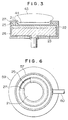
- Figs. 2 and 3 show an embodiment of the present invention in which plasma having a high density is generated in a plasma generating section and is then guided to migrate toward an area above a target disposed in a processing chamber.
- a plasma generating section A includes a pair of magnets 41, 42 for establishing a mirror magnetic field and a source 35 of microwaves.
- the mirror magnetic field is established by the magnets 41 and 42, and microwaves from the microwave source 35 are directed toward and into the chamber 37 in a relation coaxial with the mirror magnetic field.
- the microwave source 35 supplies the microwaves through a waveguide 36.
- microwaves is used to designate electromagnetic waves having a wavelength less than about 100 cm.
- electromagnetic waves having a wavelength of from about 1 cm to about 100 cm are called the microwaves.
- a microwave source of 2.45 GHz (corresponding to a wavelength of about 12 cm) is well known.
- the plasma generating chamber 37 is a waveguide in itself and hermetically communicates with a processing section B through an opening 34 to form a hermetic structure.
- the plasma generating chamber 37 is connected to the waveguide 36 for the microwave source 35 through a hermetically sealed microwave window 39 formed of a material such as quartz or alumina and through a tapered waveguide 38 tapered for the purpose of diameter matching.
- the plasma generating chamber 37 is provided with a gas inlet 40 through which a plasma-forming gas, for example, an inert gas such as Ar, Xe, He or Rn can be introduced.
- a plasma-forming gas for example, an inert gas such as Ar, Xe, He or Rn can be introduced.
- Ar or Xe is used.
- a processing chamber (described later) enclosed by a hermetic or vacuum enclosure wall 29 can be evacuated together with the plasma generating chamber 37 by an evacuating system including, for example, a cryopanel maintained at the temperature of liquid He and aided by a rotary pump, or a turbo-molecular pump.
- the vacuum is desirably oil-less and clean.
- a working gas such as Ar at a pressure of the order of 10 ⁇ 4 to 10 ⁇ 2 Torr (10 ⁇ 2 to 100 Pa) is introduced into the plasma generating chamber 37 from the gas inlet 40, and the microwaves from the microwave source 35 are directed to the working gas to generate plasma in the chamber 37.
- the microwave source 35 is a 2.45 GHz source
- the upper limit of the density of the plasma is usually 7.4 ⁇ 1010 electrons/c.c. without the aid of a magnetic field. It is to be noted that the above limit is exceeded by the utilization of a magnetic field, and plasma having a high density can be generated.
- a mirror magnetic field having a strength exceeding that required for satisfying the condition of electron cyclotron resonance (ECR) is established in parallel to the direction of the microwaves, the cut-off condition disappears, and plasma having a density as high as 1011 to 1012 electrons/c.c. can be generated.
- the pair of electromagnets 41 and 42 are provided for establishing such a mirror magnetic field, and the magnet 42 has a field strength higher than that of the magnet 41. Therefore, rightward migration of the plasma in Fig. 2 is restricted, and the plasma migrates in the direction of from the magnet 42 toward the magnet 41 (leftward in Fig. 2).
- the processing section B includes an evacuatable processing chamber enclosed by the wall 29, and, in this evacuatable processing chamber, a substrate 31 to be deposited with a thin film is disposed opposite to a target 21 made of a film-forming material and contained in an electrode structure 33.
- the substrate 31 is held in position by a substrate holder 32, and the holder 32 is supported by a supporting shaft 24. Both of the holder 32 and the shaft 24 are made of a metal material.
- the shaft 24 is hermetically fixed in position in a relation electrically insulated from the chamber wall 29.
- the electrode structure 33 is supported on a feed through post 28 which is hermetically fixed in position in a relation electrically insulated from the chamber wall 29.
- the substrate 31 may be disposed in any suitable position relative to the target 21, provided that the material sputtered out from the target 21 can be successfully deposited in thin film form on the surface of the substrate 31.
- both of the target 21 and the substrate 31 extend vertically and are disposed opposite to each other as shown.
- the electrode structure 33 does not include magnets unlike that in the prior art sputtering apparatus of the planar magnetron type.
- a cathode 23 is disposed beneath the target 21 with a backing plate 22 made of a good electrical and thermal conductor such as copper interposed therebetween, and an anode 27 is disposed around the stack of the target 21, backing plate 22 and cathode 23 with insulator members 25 and 26 interposed therebetween, so that cations can be directed perpendicularly toward and onto the surface of the target 21.
- Both of the anode 27 and the cathode 23 may be formed of a metal such as a stainless steel or aluminum.
- the target 21 is formed of a material to be deposited on the surface of the substrate 31.
- Typical examples of the material of the target 21 are a metal such as Al, W or Mo, a semiconductor such as Si, and an electrical insulator such as SiO2.
- a power source 30, e.g. a DC power source is shown connected between the anode 27 and the cathode 23 for establishing a cation-accelerating electric field above the target 21.
- an rf source is connected between the anode 27 and the cathode 23.
- the upper end of the opening 34 lies beneath the substrate 31, and its center lies above the target 21. This is because, when a portion of the opening 34 lies above the substrate 31, trouble such as etching of the substrate 31 and the film deposited thereon tends to occur, while, when the center of the opening 34 lies beneath the target 21, the highest density portion of the plasma can be hardly effectively utilized.
- the central axis of the plasma generating chamber 37 makes an angle with the surface of the target 21, it is preferable that an extension of the central axis of the chamber 37 intersects with the middle portion of the surface of the target 21.
- the DC power source 30 is described as an example of the cation-accelerating power source, it may be replaced by an rf power source.
- the rf power source is effective for preventing charge-up of the target 21.
- Other charge-up preventive means or charge neutralizing means may be combined with the power source when so desired.
- the process of deposition of a film on the substrate 31 by sputtering includes introducing, for example, Ar gas into the plasma generating chamber 37 (and the processing chamber 29) until a predetermined pressure builds up, energizing the electromagnets 41, 42 and directing the microwaves from the microwave source 35 toward and into the plasma generating chamber 37. Consequently, plasma having a high density (1011 to 1012 electrons/c.c.) is generated in the space defined principally by the mirror magnetic field in the plasma generating chamber 37. Since the strength of the right-hand portion of the mirror magnetic field is larger than that of the left-hand portion in Fig. 2, the substantial portion of the plasma diffuses leftward to migrate into the processing chamber 29.
- the plasma migrated into the processing chamber 29 diffuses over a wide area of the surface of the target 21 to cause sputtering of the material of the target 21 under influence of the electric field established in a relation substantially perpendicular to the surface of the target 21. Atoms, molecules, etc. sputtered out from the surface of the target 21 fly upward to be deposited on the surface of the substrate 31.
- Fig. 3 shows schematically the profile of the plasma 43 maintained above the target 21.
- This plasma 43 is generated in the plasma generating chamber 37 and guided to migrate toward the area above the target 21.
- the magnets disposed beneath the target in the prior art apparatus are removed, and plasma formed at a separate place is guided to migrate toward the area above the target 21. Therefore, the high-density plasma can be distributed over a wide area above the surface of the target 21, and no hollow portion occurs in the plasma unlike the prior art, planar magnetron sputtering.
- the wide area (preferably, the entire area) of the surface of the target 21 can participate in the sputtering operation.
- the quantity of atoms or particles sputtered out from the surface of the target 21 per unit time increases, and the rate of deposition of the atoms or particles on the surface of the substrate 31 also increases. Further, almost the entirety of the surface area of the target 21 is eroded to greatly increase the rate of the usable area of the target 21, and this increases the number of wafers that can be processed with a single target.
- the density of high-density plasma can be controlled by controlling the microwave source 35, and the power supply voltage applied across the anode 27 and the cathode 23 provides the ion-accelerating energy.
- the density of the plasma and the acceleration of the ions can be controlled independently, so that the optimized sputtering conditions meeting the material of the target can be selected as desired.
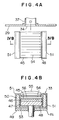
- Figs. 4A and 4B show part of another embodiment of the present invention which comprises an electrode structure exhibiting a marked confining effect on electrons in plasma guided to migrate toward the area above a target.
- the Lorentz's force produced by a magnetic field is imparted to electrons migrating toward a target from a plasma generating chamber to impart rotary motion to the electrons for trapping the electrons in the vicinity of the surface of the target.
- a magnetic field substantially parallel to the surface of the target is established.
- the structure of this second embodiment is generally similar to that of the first embodiment shown in and described with reference to Fig. 2, except its electrode structure.
- a cathode 47, a backing plate 46 and a target plate 45 are stacked in tiers to constitute a cathode structure, as in the case of Fig. 2. It will be seen in Fig. 4A that this cathode structure is rectangular in shape. This rectangular shape is advantageous over a circular shape in that a uniform magnetic field parallel to the surface of a target can more easily be produced.
- An insulator member 48 surrounds the cathode structure, and an anode structure 52 surrounds the insulator member 48.
- the anode structure 52 includes an anode base 49 and magnetic members 50, 51 disposed on the bath end edge portions respectively of the anode base 49.
- a yoke 53 magnetically coupling the magnetic members 50 and 51 is disposed between the anode base 49 and the insulator member 48.
- the yoke 53 and the magnetic members 50, 51 are magnetically coupled to constitute a magnetic circuit which is open at its upper part. By the function of this magnetic circuit, a magnetic flux distribution 54 substantially parallel to the surface of a target 45 is provided above the target 45.
- Fig. 4A electrons migrating from the plasma generating chamber 37 cross the magnetic field 54.
- the electrons are subjected to rotary motion by the Lorentz's force.
- the electrons imparted with the rotary motion are trapped in an area in the vicinity of the target 45.
- the trapped electrons impinge against neutral molecules/atoms to further promote ionization thereby maintaining the plasma at the high density.
- the high-density plasma 55 (Fig. 4B) is maintained above the surface of the target 45.
- the cations in the high-density plasma 55 are accelerated by an electric field substantially perpendicular to the surface of the target 45 to impinge against the surface of the target 45 thereby causing sputtering of atoms or particles from the surface of the target 45. These atoms or molecules deposit on the surface of a substrate (not shown) to form a thin film thereon.
- the target 45 is eroded over a widely extended region in the second embodiment of the present invention until finally the target 45 can be eroded over its entire surface region.
- the plasma maintained above the target 45 has a density higher than that in the first embodiment shown in Fig. 2, by virtue of the plasma confining effect of the magnetic field. Therefore, the film deposition by sputtering can be attained at a higher rate. Further, due to the fact that the plasma can be confined in the area adjacent to the target 45, close access of the plasma to the substrate can be prevented, thereby reducing the possibility of impingement of charged particles against the substrate and minimizing damage to the substrate.
- Figs. 5 and 6 show still another embodiment of the present invention in which a mirror magnetic field is formed directly above a target, and microwaves are directed toward plasma for attaining sputtering by erosion of a widest possible area of the surface of the target.
- this third embodiment its electrode structure and substrate supporting structure are similar to those employed in the embodiment shown in Fig. 2.
- a target 21 is backed up at its rear surface by a backing plate 22, and a cathode 23 is disposed to make intimate engagement at its front surface with the rear surface of the backing plate 22.
- An anode 27 is disposed outside of the cathode 23 with a disc-shaped insulator member 25 and a cylindrical insulator member 26 interposed therebetween.
- a feed through post 28 of the cathode 23 extends through a vacuum enclosure wall 29 to support the anode 27 and cathode 23 in an evacuatable processing chamber in a relation electrically insulated from the wall 29.
- a power source 30 is connected between the anode 27 and the cathode 23.
- a substrate 31 is disposed on a substrate holder 32 at a position opposite to the target 21.
- a shaft 24 of the substrate holder 32 extends through the vacuum enclosure wall 29 to support the substrate 31 in the evacuatable processing chamber in a relation electrically insulated from the wall 29.
- An opening 34 is provided in a portion of a vacuum enclosure wall 57 surrounding the electrode structure 33, and a waveguide 60 for microwaves is connected at one end thereof to the opening 34.
- Another waveguide 36 is connected at one end thereof to the other end of the waveguide 60 through a hermetic window 39 permeable to microwaves and at the other end thereof to a microwave source 35.
- the waveguides 36 and 60 are so disposed as to direct microwaves toward an area above the surface of the target 21.
- the window 39 is disposed at a position retracted or spaced apart from the wall 29 of the processing chamber so that the sputtered material may not deposit on the window 39 thereby obstruct introduction of the microwaves.
- the microwave introduction mechanism may be any other suitable one, provided that microwaves can be effectively directed toward the area above the target 21, and deposition of the sputtered material on the window 39 can be prevented. Although only one microwave introduction mechanism is illustrated, a plurality of such mechanisms may be disposed in radial relation.
- the axis of the microwave introduction system is arranged to be horizontal, and the lower end of the waveguide 60 aligns substantially with the upper end of the electrode structure 33, as illustrated.
- the upper limit of the density of the plasma is 7.4 ⁇ 1010 electrons/c.c. at the most.
- plasma will diffuse, and it will be unable to increase the density of the plasma in the area above the target. Therefore, a magnetic field having a strength exceeding that required for satisfying the condition of ECR is produced above the target 21.
- the target 21 and the vacuum enclosure wall 57 are preferably circular in sectional shape for producing such a magnetic flux distribution.
- annular magnets 58 and 59 are disposed outside the vacuum enclosure wall 57 at position upper and lower relative to the waveguide 60. These magnets 58 and 59 establish a mirror magnetic field so that charged particles (especially, electrons having high energy) in the plasma generated in the vicinity of the electrode structure 33 can be confined in an area near the surface of the target 21 and may not impinge against the substrate 31.
- the working gas may be introduced from any desired position provided that it can be quickly supplied toward and onto the target 21.
- it is most effective to introduce the microwaves in a relation coaxial with the axis of the magnetic field.
- the microwaves are introduced along the surface of the target 21 as shown in Fig. 5.
- the power supply voltage from the power source 30 is applied across the anode 27 and the cathode 23, and the microwaves from the microwave source 35 are introduced to generate the plasma in the area above the target 21. Electrons in the plasma are excited by the microwaves in the mirror magnetic field established by the magnets 58 and 59, thereby making cyclotron motion. Consequently, impingement between the electrons and the neutral particles is promoted to increase the density of the plasma.
- plasma having a high density is formed above the surface of the target 21.
- plasma having a controlled high density covering the entire area of the surface of the target 21 can be generated as in the case of Fig. 3.
- the ions in the plasma are accelerated to migrate toward and onto the surface of the target 21 under influence of the electric field substantially perpendicular to the target surface until the ions impinge against the surface of the target 21.
- constituent atoms or particles are sputtered out from the surface of the target 21, and the thus sputtered-out atoms or particles deposit to form a thin film on the surface of the substrate 31.
- the plasma formed in the area above the surface of the target 21 has a high density over the entire area of the surface of the target 21. Therefore, almost the entirety of the surface of the target 21 can be eroded as a result of sputtering.
- plasma having a high density can be generated in the area above the entire surface of the target 21, and almost the entirety of the surface of the target 21 can participate in the sputtering operation. Therefore, the quantity of atoms or particles sputtered out from the surface of the target 21 per unit time increases, and the rate of deposition of the atoms or particles on the surface of the substrate 31 also increases. Further, almost the entirety of the surface area of the target 21 is eroded to greatly increase the rate of the usable area of the target 21, and this increases the number of wafers that can be processed with a single target.
- the density of high-density plasma can be controlled by controlling the microwave source, and the power supply voltage applied across the anode 27 and the cathode 23 provides the ion-accelerating electric field.
- the density of the plasma and the acceleration of the ions can be controlled independently, so that the optimized sputtering conditions meeting the material of the target can be selected as desired.
Description
- This invention relates to sputtering, and more particularly to the so-called plasma sputtering according to which cations existing in plasma are accelerated by an electric field to impinge against the surface of a target thereby depositing the material of the target on the surface of a substrate or a workpiece.
- Sputtering is one of important techniques used for film deposition, e.g. in the course of manufacture of semiconductor devices. The process of sputtering includes generally ionizing an inert gas (for example, argon) to generate cations and accelerating the cations to impinge against the surface of a target, thereby causing emission of constituent atoms or molecules from the target and depositing the liberated atoms or molecules on the surface of a substrate disposed opposite to the target. The deposition rate or speed is dependent upon the number of ions incident on the surface of the target and the sputtering yield of the ions. It is effective to utilize plasma at a high density for increasing the number of incident ions.
- Planar magnetron sputtering is known in which a target is disposed on or above a cathode, and a central magnetic pole member and a peripheral magnetic pole member are disposed in the cathode disposed underneath the target. There is formed a closed loop of magnetic field in the electrode structure. Due to the above arrangement, arcuate lines of magnetic force extending through the target in the thicknesswise direction thereof appear between the central magnetic pole member and the peripheral magnetic pole member. These magnetic lines of force flow in the radial direction when viewed from the upside of the target. The central portion of the magnetic lines of force forms an upward convex arc on the surface of the target. In other words, the profile of the magnetic lines of force on the target is analogous to that of a doughnut truncated in its lower portion. Plasma is produced when the electric field is built up by the electrode structure in the presence of a low-pressure gas introduced into such a magnetic field, and electrons tending to migrate outward from the doughnut-like portion are deflected by the magnetic field to be confined within the extent of the magnetic field distribution. These electrons contribute to further ionization of the gas molecules. Thus, high-density plasma in the form of a doughnut (toroidal ring) or a hollow circle (loop) is produced on the target. Cations (inert gas ions) in the plasma are accelerated toward the target by the electric field to effect sputtering. As a result, the corresponding area of the target is eroded in the form of a hollow ring or loop.
- According to this method, the target is eroded in its local area only. Therefore, the ratio of the sputtering-participating area to the entire area of the surface of the target (the target utilization efficiency) is low, the deposition rate is low, and the useful service life of the target is short.
- A proposal for changing the diameter of the magnetic flux distribution thereby widening the eroded surface area of the target has been made, as disclosed, for example, in USP 4,401,539 assigned to the present assignee. According to the proposal, however, only a limited portion of the surface area of the target is utilized for sputtering at a moment. It has therefore been strongly demanded to develop a method and apparatus which can more effectively utilize the target so that the entire surface area of the target can serve as a source of vaporization or sputtering. FR-A-2,324,755 discloses an apparatus and a method of sputtering in which a magnetic field is applied parallel to a surface above which the plasma is confined. DE-A-3,144,016 discloses a plasma processing apparatus where a plasma stream produced by microwave is transferred using magnetic means.
- Further, in JP-A-58-75839 there is disclosed a sputtering apparatus for forming a high-density torus plasma on a target by a magnetic field in which microwave is introduced in the vicinity of a gas inlet of a processing chamber so as to increase the plasma density and the processing rate.
- It is a primary object of the present invention to provide a sputtering method and apparatus which can utilize a possible wide surface area of a target for attaining sputtering without locally eroding the target in the pattern of a hollow ring or loop.
- For the purpose of attaining sputtering with the material vaporized from a widest possible area of a target without causing local erosion of the target, employment of magnets such as those employed in the prior art planar magnetron sputtering is not desirable. On the other hand, however, it is difficult to increase the density of plasma without the aid of a magnetic field. In the case of the prior art planar magnetron sputtering which utilizes magnetic lines of force emanating through a target, drawing an arc above the target and terminating to flow through the target again, high-density plasma has been produced only on a portion of the target (corresponding to the bulged portion of the arc of the magnetic lines of force on the target). In contrast, the inventors contemplate to generate a magnetic field of such a configuration which does not substantially include magnetic lines of force traversing a target and forming closed loops in an electrode structure, so that high-density plasma can be produced in the magnetic field of the above configuration for the purpose of effecting efficient sputtering. According to an aspect of the present invention, the combination of a mirror magnetic field and a source of microwave is used to produce high-density plasma thereby efficiently sputtering the material of a target on the surface of a substrate. The mirror magnetic field can be produced by a pair of magnets. When such two magnets are arranged on a single axis in coaxial relation, a magnetic flux distribution is obtained in which the lines of magnetic flux expand or bulge in the region intermediate between the magnets and are constricted in the regions close to the magnets. By utilizing such mirror magnetic flux and directing microwaves toward the intermediate expanding flux region, high-density plasma can be produced to be confined in the expanding flux region. Further, the density of the plasma can be made very high, unlike the case where such a mirror magnetic field is not present. In an aspect, the high-density plasma produced at a place remote from the target is guided toward the target to be maintained in an area above the target. In another aspect, the high-density plasma is directly produced and maintained in an area above the target.
- According to the present invention, as defined in the
main claims 1, 10 and 20 the high-density plasma can thus be maintained above the target over a wide surface area of the target. Also, by virtue of the fact that the energy of ions impinging against the target can be controlled independently of the emission of the plasma, the optimized sputtering conditions can be selected as desired to meet the material of the target. The capability of attaining desired sputtering of material over the wide surface area of the target can greatly increase the rate of film deposition by sputtering and can also greatly improve the rate of utilization of the target. Also, the capability of selecting the optimized sputtering conditions meeting the material of the target improves the efficiency of production and also improves the rate of utilization of material as well as the performance of semiconductor devices. - Other objects, features and advantages of the present invention will become apparent from the following detailed description of preferred embodiments thereof taken in conjunction with the accompanying drawings, in which:
- Fig. 1A is a schematic sectional view of a prior art, planar magnetron sputtering apparatus;
- Fig. 1B is an enlarged partial view of the electrode structure in Fig. 1A to show how a target plate is eroded;
- Fig. 2 is a diagrammatic sectional view of an embodiment of the sputtering apparatus according to the present invention;
- Fig. 3 is a sectional view showing schematically the profile of plasma generated on the target shown in Fig. 2;
- Fig. 4A is a schematic top plan view of part of another embodiment of the sputtering apparatus according to the present invention;
- Fig. 4B is a schematic sectional view taken along the line IVB-IVB in Fig. 4A;
- Fig. 5 is a diagrammatic sectional view of still another embodiment of the sputtering apparatus according to the present invention;
- Fig. 6 is a top plan view of part of the apparatus shown in Fig. 5.
- For a better understanding of the present invention, the prior art will be first described before describing the present invention in detail.
- Figs. 1A and 1B show schematically the structure of a prior art, planar magnetron sputtering apparatus.
- Referring to Figs. 1A and 1B, a target plate (referred to hereinafter merely as a target) 1 is backed up at its rear surface by a
backing plate 2. Disposed on the rear surface side of thebacking plate 2 are a peripheral annularmagnetic pole member 4 and a central solid cylindricalmagnetic pole member 5 which are magnetically coupled to each other by ayoke 3 to constitute a magnetic circuit. The target 1 and thebacking plate 2 are made of non-magnetic materials respectively, and the lines of magnetic flux flowing between the magnetic members draw an arc extending through the target 1 in the thicknesswise direction of the target 1 as shown in Fig. 1B. Acathode 6 encloses themagnetic members yoke 3 therein and is hermetically closed by thebacking plate 2. Ashield 8 is mounted on the outer peripheral portion of thecathode 6 with an annularinsulating member 7 interposed therebetween. Thecathode 6 is supported on ashaft 10 which is electrically insulated from and hermetically secured to a hermetic orvacuum enclosure wall 9 of a vacuum chamber. An anode 11 is disposed above thecathode 6, and apower source 12 is connected between the anode 11 and thecathode 6. - In the prior art sputtering apparatus having the structure described above, the lines of magnetic force in the vicinity of the surface of the target 1 are distributed to provide a doughnut-like or semi-annular
magnetic field distribution 13 as best seen in Fig. 1B. Application of the power supply voltage across the anode 11 and thecathode 6 generates plasma. The semi-annularmagnetic field distribution 13 acts to confine the plasma so that the plasma has a high density in atoroidal ring region 14 shown in Fig. 1B. The ions in the plasma are accelerated by an electric field substantially perpendicular to the surface of the target 1 to impinge against the surface of the target 1. As a result, some or more of the constituent atoms or particles are sputtered out from the surface of the target 1 to leave a locally eroded or etchedregion 15 on the target surface. The atoms or particles sputtered out from the surface of the target 1 migrate toward and onto the lower surface of asubstrate 17 supported on asubstrate stage 16 to deposit and form a thin film on the lower surface of thesubstrate 17. - The eroded or etched
region 15 on the surface of the target 1 is progressively widened with time due to repetition of the sputtering process. However, this erosion is generally limited to a specific region on the surface of the target 1 in the target arrangement shown in Fig. 1B. - It will be seen from the above description that, in the prior art sputtering apparatus of the planar magnetion type, the plasma has a high density above a limited region only of the surface of the target 1, and progressive erosion of the target 1 due to repeated sputtering is limited to a specific region only of the target 1. Because of the limited small area of the source of sputtering, the rate of deposition of the target material on the
substrate 17 cannot be increased, and the rate of utilization of the target surface is also low. Also, due to the progressive erosion of a limited region only of the target 1 with time due to repetition of the sputtering process, it has been necessary to replace the target 1 when the specific region has been eroded by a predetermined quantity or limit, resulting in a short usable life of the target. - The present invention eliminates the use of the magnets disposed beneath the target in the electrode structure of the prior art magnetron sputtering apparatus and yet attains the formation of high-density plasma over a wide area of the surface of the target. More precisely, according to the present invention, high-density plasma covering a substantial area of the surface of the target is generated without resorting to the use of a magnetic field forming a closed loop of magnetic flux extending through the target in the thicknesswise direction of the target.
- Plasma having a high density is generated with the use of a magnetic field not forming a closed loop inside the electrode structure which contains the target, unlike the prior art, and the plasma is maintained above the target to cover a wide area of the surface of the target for effecting desired sputtering. According to one aspect of the present invention, magnets for establishing a mirror magnetic field are disposed at a place remote from a target, and microwaves are introduced toward and into the space defined by the lines of magnetic force of the mirror magnetic field thereby generating plasma having a high density.
- The space defined by the magnetic lines of force of the mirror magnetic field (the intermediate bulged portion of the magnetic flux) exhibits a confinement effect on the plasma.
- The electrode structure in the present invention includes an anode and a cathode (a power source is to be connected therebetween), and a target is supported on the cathode. Therefore, an electric field substantially perpendicular to the surface of the target is produced. Cations existing above the target are accelerated by the electric field to impinge against the target.
- The absence of any magnetic lines of force forming a closed loop in the electrode structure which contains the target is equivalent to or indicates the absence of a magnetic flux distribution drawing an arc above the target and having a bulged portion extending adjacent to a limited region only of the target. Therefore, a limited region only of the target is not eroded unlike that employed in the prior art sputtering apparatus of the planar magnetron type. The high-density plasma is generated by the aid of the mirror magnetic field, but the plasma is not localized to a limited region only of the target.
- The high-density plasma is maintained in an area above the target according to, for example, one of the following manners: (1) The high-density plasma is generated at a place distant from the target by the combination of a mirror magnetic field and microwaves, and the thus generated high-density plasma is guided to migrate toward an area above the target. (2) Plasma migrated according to the method (1) is confined in a magnetic field whose lines of force do not penetrate the target and are in parallel to the surface of the target. (3) A mirror magnetic field is established in an area close to the target in such a relation that the lines of force or magnetic flux penetrate the entire surface of the target, and microwaves are directed toward and into the space defined by the mirror magnetic field.
- Figs. 2 and 3 show an embodiment of the present invention in which plasma having a high density is generated in a plasma generating section and is then guided to migrate toward an area above a target disposed in a processing chamber.
- Referring to Fig. 2, a plasma generating section A includes a pair of
magnets source 35 of microwaves. In aplasma generating chamber 37, the mirror magnetic field is established by themagnets microwave source 35 are directed toward and into thechamber 37 in a relation coaxial with the mirror magnetic field. - The
microwave source 35 supplies the microwaves through awaveguide 36. Herein, the term "microwaves" is used to designate electromagnetic waves having a wavelength less than about 100 cm. Generally, electromagnetic waves having a wavelength of from about 1 cm to about 100 cm are called the microwaves. As a typical example of commercially available sources, a microwave source of 2.45 GHz (corresponding to a wavelength of about 12 cm) is well known. Theplasma generating chamber 37 is a waveguide in itself and hermetically communicates with a processing section B through anopening 34 to form a hermetic structure. Theplasma generating chamber 37 is connected to thewaveguide 36 for themicrowave source 35 through a hermetically sealedmicrowave window 39 formed of a material such as quartz or alumina and through a taperedwaveguide 38 tapered for the purpose of diameter matching. Theplasma generating chamber 37 is provided with agas inlet 40 through which a plasma-forming gas, for example, an inert gas such as Ar, Xe, He or Rn can be introduced. Preferably, Ar or Xe is used. - A processing chamber (described later) enclosed by a hermetic or
vacuum enclosure wall 29 can be evacuated together with theplasma generating chamber 37 by an evacuating system including, for example, a cryopanel maintained at the temperature of liquid He and aided by a rotary pump, or a turbo-molecular pump. The vacuum is desirably oil-less and clean. After the step of evacuation, a working gas such as Ar at a pressure of the order of 10⁻⁴ to 10⁻² Torr (10⁻² to 10⁰ Pa) is introduced into theplasma generating chamber 37 from thegas inlet 40, and the microwaves from themicrowave source 35 are directed to the working gas to generate plasma in thechamber 37. When themicrowave source 35 is a 2.45 GHz source, the upper limit of the density of the plasma is usually 7.4 × 10¹⁰ electrons/c.c. without the aid of a magnetic field. It is to be noted that the above limit is exceeded by the utilization of a magnetic field, and plasma having a high density can be generated. Thus, when a mirror magnetic field having a strength exceeding that required for satisfying the condition of electron cyclotron resonance (ECR) is established in parallel to the direction of the microwaves, the cut-off condition disappears, and plasma having a density as high as 10¹¹ to 10¹² electrons/c.c. can be generated. - The pair of
electromagnets magnet 42 has a field strength higher than that of themagnet 41. Therefore, rightward migration of the plasma in Fig. 2 is restricted, and the plasma migrates in the direction of from themagnet 42 toward the magnet 41 (leftward in Fig. 2). - The processing section B includes an evacuatable processing chamber enclosed by the
wall 29, and, in this evacuatable processing chamber, asubstrate 31 to be deposited with a thin film is disposed opposite to atarget 21 made of a film-forming material and contained in anelectrode structure 33. - The
substrate 31 is held in position by asubstrate holder 32, and theholder 32 is supported by a supportingshaft 24. Both of theholder 32 and theshaft 24 are made of a metal material. Theshaft 24 is hermetically fixed in position in a relation electrically insulated from thechamber wall 29. Theelectrode structure 33 is supported on a feed throughpost 28 which is hermetically fixed in position in a relation electrically insulated from thechamber wall 29. Thesubstrate 31 may be disposed in any suitable position relative to thetarget 21, provided that the material sputtered out from thetarget 21 can be successfully deposited in thin film form on the surface of thesubstrate 31. Preferably, both of thetarget 21 and thesubstrate 31 extend vertically and are disposed opposite to each other as shown. - The
electrode structure 33 does not include magnets unlike that in the prior art sputtering apparatus of the planar magnetron type. Acathode 23 is disposed beneath thetarget 21 with abacking plate 22 made of a good electrical and thermal conductor such as copper interposed therebetween, and ananode 27 is disposed around the stack of thetarget 21, backingplate 22 andcathode 23 withinsulator members target 21. Both of theanode 27 and thecathode 23 may be formed of a metal such as a stainless steel or aluminum. - The
target 21 is formed of a material to be deposited on the surface of thesubstrate 31. Typical examples of the material of thetarget 21 are a metal such as Al, W or Mo, a semiconductor such as Si, and an electrical insulator such as SiO₂. In Fig. 2, apower source 30, e.g. a DC power source, is shown connected between theanode 27 and thecathode 23 for establishing a cation-accelerating electric field above thetarget 21. When the target is formed of an insulator such as SiO₂, an rf source is connected between theanode 27 and thecathode 23. - When the central axis of the plasma generating chamber 37 (or the central axis of the magnetic field or of the microwaves) is parallel to the target surface, it is preferable that the upper end of the
opening 34 lies beneath thesubstrate 31, and its center lies above thetarget 21. This is because, when a portion of theopening 34 lies above thesubstrate 31, trouble such as etching of thesubstrate 31 and the film deposited thereon tends to occur, while, when the center of theopening 34 lies beneath thetarget 21, the highest density portion of the plasma can be hardly effectively utilized. - On the other hand, when the central axis of the
plasma generating chamber 37 makes an angle with the surface of thetarget 21, it is preferable that an extension of the central axis of thechamber 37 intersects with the middle portion of the surface of thetarget 21. - Although the
DC power source 30 is described as an example of the cation-accelerating power source, it may be replaced by an rf power source. Especially, when the material of thetarget 21 is an electrical insulator, the rf power source is effective for preventing charge-up of thetarget 21. Other charge-up preventive means or charge neutralizing means may be combined with the power source when so desired. - The process of deposition of a film on the
substrate 31 by sputtering includes introducing, for example, Ar gas into the plasma generating chamber 37 (and the processing chamber 29) until a predetermined pressure builds up, energizing theelectromagnets microwave source 35 toward and into theplasma generating chamber 37. Consequently, plasma having a high density (10¹¹ to 10¹² electrons/c.c.) is generated in the space defined principally by the mirror magnetic field in theplasma generating chamber 37. Since the strength of the right-hand portion of the mirror magnetic field is larger than that of the left-hand portion in Fig. 2, the substantial portion of the plasma diffuses leftward to migrate into theprocessing chamber 29. The plasma migrated into theprocessing chamber 29 diffuses over a wide area of the surface of thetarget 21 to cause sputtering of the material of thetarget 21 under influence of the electric field established in a relation substantially perpendicular to the surface of thetarget 21. Atoms, molecules, etc. sputtered out from the surface of thetarget 21 fly upward to be deposited on the surface of thesubstrate 31. - Fig. 3 shows schematically the profile of the
plasma 43 maintained above thetarget 21. Thisplasma 43 is generated in theplasma generating chamber 37 and guided to migrate toward the area above thetarget 21. In the present invention, the magnets disposed beneath the target in the prior art apparatus are removed, and plasma formed at a separate place is guided to migrate toward the area above thetarget 21. Therefore, the high-density plasma can be distributed over a wide area above the surface of thetarget 21, and no hollow portion occurs in the plasma unlike the prior art, planar magnetron sputtering. According to the first embodiment of the present invention, the wide area (preferably, the entire area) of the surface of thetarget 21 can participate in the sputtering operation. Therefore, the quantity of atoms or particles sputtered out from the surface of thetarget 21 per unit time increases, and the rate of deposition of the atoms or particles on the surface of thesubstrate 31 also increases. Further, almost the entirety of the surface area of thetarget 21 is eroded to greatly increase the rate of the usable area of thetarget 21, and this increases the number of wafers that can be processed with a single target. - Further, according to the embodiment of the present invention, the density of high-density plasma can be controlled by controlling the
microwave source 35, and the power supply voltage applied across theanode 27 and thecathode 23 provides the ion-accelerating energy. Thus, the density of the plasma and the acceleration of the ions can be controlled independently, so that the optimized sputtering conditions meeting the material of the target can be selected as desired. - In the embodiment of the present invention, there is not any substantial confining effect on the plasma guided to migrate to the area above the target. Although the perpendicular electric field on the target acts to accelerate the cations toward and onto the target, its confining effect on the electrons is not marked.
- Figs. 4A and 4B show part of another embodiment of the present invention which comprises an electrode structure exhibiting a marked confining effect on electrons in plasma guided to migrate toward the area above a target. In this second embodiment, the Lorentz's force produced by a magnetic field is imparted to electrons migrating toward a target from a plasma generating chamber to impart rotary motion to the electrons for trapping the electrons in the vicinity of the surface of the target. For this purpose, a magnetic field substantially parallel to the surface of the target is established. The structure of this second embodiment is generally similar to that of the first embodiment shown in and described with reference to Fig. 2, except its electrode structure.
- Referring to Fig. 4B, a
cathode 47, abacking plate 46 and atarget plate 45 are stacked in tiers to constitute a cathode structure, as in the case of Fig. 2. It will be seen in Fig. 4A that this cathode structure is rectangular in shape. This rectangular shape is advantageous over a circular shape in that a uniform magnetic field parallel to the surface of a target can more easily be produced. - An
insulator member 48 surrounds the cathode structure, and ananode structure 52 surrounds theinsulator member 48. Theanode structure 52 includes ananode base 49 andmagnetic members anode base 49. Ayoke 53 magnetically coupling themagnetic members anode base 49 and theinsulator member 48. Theyoke 53 and themagnetic members magnetic flux distribution 54 substantially parallel to the surface of atarget 45 is provided above thetarget 45. - Referring to Fig. 4A, electrons migrating from the
plasma generating chamber 37 cross themagnetic field 54. The electrons are subjected to rotary motion by the Lorentz's force. As a result, the electrons imparted with the rotary motion are trapped in an area in the vicinity of thetarget 45. The trapped electrons impinge against neutral molecules/atoms to further promote ionization thereby maintaining the plasma at the high density. Thus, the high-density plasma 55 (Fig. 4B) is maintained above the surface of thetarget 45. The cations in the high-density plasma 55 are accelerated by an electric field substantially perpendicular to the surface of thetarget 45 to impinge against the surface of thetarget 45 thereby causing sputtering of atoms or particles from the surface of thetarget 45. These atoms or molecules deposit on the surface of a substrate (not shown) to form a thin film thereon. - As shown at 56 in Fig. 4B, the
target 45 is eroded over a widely extended region in the second embodiment of the present invention until finally thetarget 45 can be eroded over its entire surface region. Also, according to the second embodiment, the plasma maintained above thetarget 45 has a density higher than that in the first embodiment shown in Fig. 2, by virtue of the plasma confining effect of the magnetic field. Therefore, the film deposition by sputtering can be attained at a higher rate. Further, due to the fact that the plasma can be confined in the area adjacent to thetarget 45, close access of the plasma to the substrate can be prevented, thereby reducing the possibility of impingement of charged particles against the substrate and minimizing damage to the substrate. - Figs. 5 and 6 show still another embodiment of the present invention in which a mirror magnetic field is formed directly above a target, and microwaves are directed toward plasma for attaining sputtering by erosion of a widest possible area of the surface of the target. In this third embodiment, its electrode structure and substrate supporting structure are similar to those employed in the embodiment shown in Fig. 2.
- Referring to Figs. 5 and 6, a
target 21 is backed up at its rear surface by abacking plate 22, and acathode 23 is disposed to make intimate engagement at its front surface with the rear surface of thebacking plate 22. Ananode 27 is disposed outside of thecathode 23 with a disc-shapedinsulator member 25 and acylindrical insulator member 26 interposed therebetween. - A feed through
post 28 of thecathode 23 extends through avacuum enclosure wall 29 to support theanode 27 andcathode 23 in an evacuatable processing chamber in a relation electrically insulated from thewall 29. Apower source 30 is connected between theanode 27 and thecathode 23. - A
substrate 31 is disposed on asubstrate holder 32 at a position opposite to thetarget 21. Ashaft 24 of thesubstrate holder 32 extends through thevacuum enclosure wall 29 to support thesubstrate 31 in the evacuatable processing chamber in a relation electrically insulated from thewall 29. Anopening 34 is provided in a portion of avacuum enclosure wall 57 surrounding theelectrode structure 33, and awaveguide 60 for microwaves is connected at one end thereof to theopening 34. Anotherwaveguide 36 is connected at one end thereof to the other end of thewaveguide 60 through ahermetic window 39 permeable to microwaves and at the other end thereof to amicrowave source 35. Thewaveguides target 21. Thewindow 39 is disposed at a position retracted or spaced apart from thewall 29 of the processing chamber so that the sputtered material may not deposit on thewindow 39 thereby obstruct introduction of the microwaves. The microwave introduction mechanism may be any other suitable one, provided that microwaves can be effectively directed toward the area above thetarget 21, and deposition of the sputtered material on thewindow 39 can be prevented. Although only one microwave introduction mechanism is illustrated, a plurality of such mechanisms may be disposed in radial relation. Typically, the axis of the microwave introduction system is arranged to be horizontal, and the lower end of thewaveguide 60 aligns substantially with the upper end of theelectrode structure 33, as illustrated. - In the absence of any magnetic field, the upper limit of the density of the plasma is 7.4 × 10¹⁰ electrons/c.c. at the most. In the absence of the magnetic field, plasma will diffuse, and it will be unable to increase the density of the plasma in the area above the target. Therefore, a magnetic field having a strength exceeding that required for satisfying the condition of ECR is produced above the
target 21. In order to form the plasma over a wide range including the entire surface area of thetarget 21, it is preferable to dispose magnets outside of theelectrode structure 33, preferably, outside of thecylindrical wall 29 of the processing chamber, thereby producing a mirror magnetic field which is coaxial with the normal extending through the center of thetarget 21. Thetarget 21 and thevacuum enclosure wall 57 are preferably circular in sectional shape for producing such a magnetic flux distribution. - Referring to Fig. 5,
annular magnets vacuum enclosure wall 57 at position upper and lower relative to thewaveguide 60. Thesemagnets electrode structure 33 can be confined in an area near the surface of thetarget 21 and may not impinge against thesubstrate 31. - The working gas may be introduced from any desired position provided that it can be quickly supplied toward and onto the
target 21. For the purpose of excitation of the plasma, it is most effective to introduce the microwaves in a relation coaxial with the axis of the magnetic field. However, in the case of the third embodiment in which the mirror magnetic field is produced in coaxial relation with the central axes of thetarget 21 andsubstrate 31 disposed opposite to each other, it is almost impossible to direct the microwaves in coaxial relation with the mirror magnetic field. In this case, therefore, according to the invention the microwaves are introduced along the surface of thetarget 21 as shown in Fig. 5. - In operation, the power supply voltage from the
power source 30 is applied across theanode 27 and thecathode 23, and the microwaves from themicrowave source 35 are introduced to generate the plasma in the area above thetarget 21. Electrons in the plasma are excited by the microwaves in the mirror magnetic field established by themagnets - In this manner, plasma having a high density is formed above the surface of the
target 21. By controlling the factor, for example, the profile of the mirror magnetic field, plasma having a controlled high density covering the entire area of the surface of thetarget 21 can be generated as in the case of Fig. 3. The ions in the plasma are accelerated to migrate toward and onto the surface of thetarget 21 under influence of the electric field substantially perpendicular to the target surface until the ions impinge against the surface of thetarget 21. As a result, constituent atoms or particles are sputtered out from the surface of thetarget 21, and the thus sputtered-out atoms or particles deposit to form a thin film on the surface of thesubstrate 31. - The plasma formed in the area above the surface of the
target 21 has a high density over the entire area of the surface of thetarget 21. Therefore, almost the entirety of the surface of thetarget 21 can be eroded as a result of sputtering. - According to the third embodiment of the present invention, plasma having a high density can be generated in the area above the entire surface of the
target 21, and almost the entirety of the surface of thetarget 21 can participate in the sputtering operation. Therefore, the quantity of atoms or particles sputtered out from the surface of thetarget 21 per unit time increases, and the rate of deposition of the atoms or particles on the surface of thesubstrate 31 also increases. Further, almost the entirety of the surface area of thetarget 21 is eroded to greatly increase the rate of the usable area of thetarget 21, and this increases the number of wafers that can be processed with a single target. - Also, according to the third embodiment of the present invention, the density of high-density plasma can be controlled by controlling the microwave source, and the power supply voltage applied across the
anode 27 and thecathode 23 provides the ion-accelerating electric field. Thus, the density of the plasma and the acceleration of the ions can be controlled independently, so that the optimized sputtering conditions meeting the material of the target can be selected as desired.
Claims (21)
- A method of sputtering including the steps of- disposing an electrode structure (33; 47, 52) carrying a planar target (21; 45) opposite to a substrate (31), said planar target being placed under a predetermined pressure condition in a processing chamber (29) and a surface of said planar target being opposed to a surface of said substrate,- causing sputtering of target material from said target (21; 45) by the action of a plasma for the deposition of a thin film on the surface of said substrate (31),- maintaining said plasma at a high density in an area above said surface of said target (21; 45) using magnetic fields defined through magnet means (41, 42; 58, 59) and microwaves which are introduced from a direction along said surface of said target,
and- accelerating ions in said plasma toward and onto the surface of said target (21; 45) by the action of an electric field established by said electrode structure (33; 47, 52) to cause impingement of ions against the surface of said target thereby causing said sputtering of said target material from said target for the deposition of said thin film on the surface of said substrate (31),said method being characterised in that it further comprises the steps of- disposing a pair of magnets (41, 42; 58, 59) outside of said electrode structure (33; 47, 52) so as to produce a mirror magnetic field and directing microwaves toward and into the space defined by said mirror magnetic field, thereby generating said high-density plasma in said space,- guiding said high-density plasma to migrate from where it is produced to a wide space above said target (21; 45),
and- sputtering said target (21; 45) by said high-density plasma in said wide space so as to sputter said target (21; 45) in a wide area of said surface of said target. - A method according to claim 1,
characterised in
that said mirror magnetic field has magnetic lines of force of a configuration covering said target (21) for trapping electrons in an area near said target. - A method according to claim 1 or 2,
characterised in
that the magnetic lines of force of said mirror magnetic field do not substantially form a closed loop inside said electrode structure (33) carrying said target (21). - A method according to claim 1,
characterised in
that said mirror magnetic field is formed in a plasma generating chamber (37) disposed adjacent to a processing chamber (29) wherein said electrode structure (33) and said substrate (31) are placed. - A method according to claim 4,
characterised in
that said plasma generating chamber (37) includes an opening (34) open toward a point above said target (21) and communicates with a microwave source (35) through a microwave-permeable window (39) disposed between said pair of magnets (41, 42) generating said mirror magnetic field. - A method according to claim 5,
characterised in
that said mirror magnetic field has a strength greater than the value required for satisfying the condition of electron cyclotron resonance with the microwaves used, said strength being larger on the side of said window (39) than on the side of said opening (34). - A method according to claim 6,
characterised in
that it further comprises the step of- generating a magnetic field along the surface of said target (45) for accelerating migrating electrons toward said target and trapping said electrons in an area near said target. - A method according to claim 6 or 7,
characterised in
that the axis of said plasma generating chamber (37) extends horizontally and runs above said target (21). - A method according to claim 1,
characterised in
that said space is defined in the vicinity of the surface of said target (21)
and
that said pair of magnets (58, 59) for generating said mirror magnetic field are disposed around said processing chamber (29) containing said electrode structure (33) and said substrate (31) therein. - A sputtering apparatus including- an electrode structure (33; 47, 52) carrying a planar target (21; 45) thereon,- a substrate supporting structure (32) supporting a substrate (31) opposite to said target (21)
and- means for generating a high-density plasma for causing sputtering of target material from said target (21) for the deposition of a thin film on the surface of said substrate (31),characterised in
that said apparatus further comprises- a pair of magnets (41, 41; 58, 59) disposed at a place apart from said electrode structure (33; 47, 52) for establishing a mirror magnetic field defining a high-density plasma generating space and- a microwave source (35) directing microwaves toward and into said high-density plasma generating space in a direction parallel to the surface of said target (21) and along the surface of said target (21),said mirror magnetic field and said microwave source (35) acting in combination to provide the high-density plasma above the target (21) over a wide surface area thereof. - A sputtering apparatus according to claim 10,
characterised in
that said high-density plasma generating space is defined in an area
near the surface of said target (21)
and
that said pair of magnets 41, 42; 58, 59) are spaced apart in the direction of the normal to the center of said target (21) in a relation coaxial to said normal. - A sputtering apparatus according to claim 10,
characterised in
that said mirror magnetic field has a strength greater than that required for satisfying the condition of electron cyclotron resonance of said microwaves. - A sputtering apparatus according to claim 10,
characterised in
that said high-density plasma generating space is defined at a place remote from said electrode structure (33)
and
that said pair of magnets (41, 42) and said microwave source (35) are disposed around said high-density plasma generating space so that said mirror magnetic field is substantially coaxial with the microwaves. - A sputtering apparatus according to claim 11,
characterised in
that said microwave source (35) is disposed so as to direct the microwaves toward a position above said target (21) and along the surface thereof. - A sputtering apparatus according to claim 13,
characterised in
that said high-density plasma generating space is defined in a waveguide (37) having an opening (34) open toward said target (21). - A sputtering apparatus according to 15,
characterised in
that said pair of magnets (41, 42) are disposed along the longitudinal direction of said waveguide (37) in coaxial relation thereto
and
that the magnet (42) which is remoter from said target (21) generates a magnetic field which has a greater strength than that generated by the magnet (41) which is closer to said target (21). - A sputtering apparatus according to claim 16,
characterised in
that said target (21) is disposed in horizontal relation
and
that said waveguide (37) also disposed in horizontal relation has its upper end lower than the surface of said substrate (31) and its central axis higher than the surface of said target (21). - A sputtering apparatus according to claim 16 or 17,
characterised in
that said waveguide (37) has its central axis extending substantially toward an area above said target (21). - A sputtering apparatus according to claim 17,
characterised in
that said electrode structure includes a cathode (47) disposed beneath said target (21) and a pair of magnets (50, 51) disposed on the opposite two sides of said target (21), said pair of magnets generating a magnetic field which is substantially parallel to the surface of said target (21) and is directed so that electrons migrating through said waveguide (37) are given a rotary motion. - A sputtering apparatus assisted with microwave power source, comprising- a cathode and a substrate holder, said cathode adapted to hold a planar target composed of a material that is to be sputtered, the substrate holder adapted to hold a substrate in a manner to be opposed to said target
and- a plasma introducing window, a microwave power source, said microwave power source being adapted to provide microwaves in a direction parallel to the surface of said planar target, and magnet means remote from said cathode for generating a plasma in combination with said microwave power source for sputtering said target, said magnet means being adapted to generate a magnetic field which transfers sideways said plasma into a space between said target and said substrate holder. - A sputtering apparatus according to claim 20,
characterised in
that said microwave is introduced through said window from a direction parallel to the surface of said target into space between said target and said substrate holder
and
that said magnet means are positioned outside and surround a chamber wherein said cathode and said substrate holder are placed, said magnet means generating a magnetic field whereby producing a plasma in combination with said microwave introduced into said magnetic field and said magnetic means confining said plasma adjacent said surface of said target.
Applications Claiming Priority (2)
| Application Number | Priority Date | Filing Date | Title |
|---|---|---|---|
| JP58243870A JPH0627323B2 (en) | 1983-12-26 | 1983-12-26 | Sputtering method and apparatus |
| JP243870/83 | 1983-12-26 |
Publications (4)
| Publication Number | Publication Date |
|---|---|
| EP0148504A2 EP0148504A2 (en) | 1985-07-17 |
| EP0148504A3 EP0148504A3 (en) | 1987-10-07 |
| EP0148504B1 EP0148504B1 (en) | 1990-11-22 |
| EP0148504B2 true EP0148504B2 (en) | 1995-07-12 |
Family
ID=17110200
Family Applications (1)
| Application Number | Title | Priority Date | Filing Date |
|---|---|---|---|
| EP84116391A Expired - Lifetime EP0148504B2 (en) | 1983-12-26 | 1984-12-27 | Method and apparatus for sputtering |
Country Status (5)
| Country | Link |
|---|---|
| US (1) | US4610770A (en) |
| EP (1) | EP0148504B2 (en) |
| JP (1) | JPH0627323B2 (en) |
| KR (1) | KR890004880B1 (en) |
| DE (1) | DE3483647D1 (en) |
Families Citing this family (60)
| Publication number | Priority date | Publication date | Assignee | Title |
|---|---|---|---|---|
| JPH0627323B2 (en) | 1983-12-26 | 1994-04-13 | 株式会社日立製作所 | Sputtering method and apparatus |
| JPS6113626A (en) * | 1984-06-29 | 1986-01-21 | Hitachi Ltd | Plasma processor |
| DE3566194D1 (en) * | 1984-08-31 | 1988-12-15 | Hitachi Ltd | Microwave assisting sputtering |
| US4842707A (en) * | 1986-06-23 | 1989-06-27 | Oki Electric Industry Co., Ltd. | Dry process apparatus |
| JPS6324030A (en) * | 1986-06-26 | 1988-02-01 | Res Dev Corp Of Japan | Anisotropic rare earth magnet material and its production |
| JPS6376867A (en) * | 1986-09-19 | 1988-04-07 | Mitsubishi Kasei Corp | Reactive sputtering device |
| JP2587924B2 (en) * | 1986-10-11 | 1997-03-05 | 日本電信電話株式会社 | Thin film forming equipment |
| JP2631650B2 (en) * | 1986-12-05 | 1997-07-16 | アネルバ株式会社 | Vacuum equipment |
| JPH066786B2 (en) * | 1987-03-17 | 1994-01-26 | 日本電信電話株式会社 | Thin film forming equipment |
| US4834860A (en) * | 1987-07-01 | 1989-05-30 | The Boc Group, Inc. | Magnetron sputtering targets |
| DE3803355A1 (en) * | 1988-02-05 | 1989-08-17 | Leybold Ag | PARTICLE SOURCE FOR A REACTIVE ION BEAM OR PLASMA POSITIONING PLANT |
| US5180436A (en) * | 1988-07-26 | 1993-01-19 | Matsushita Electric Industrial Co., Ltd. | Microwave plasma film deposition system |
| US5125358A (en) * | 1988-07-26 | 1992-06-30 | Matsushita Electric Industrial Co., Ltd. | Microwave plasma film deposition system |
| US4952273A (en) * | 1988-09-21 | 1990-08-28 | Microscience, Inc. | Plasma generation in electron cyclotron resonance |
| JPH0689446B2 (en) * | 1988-12-19 | 1994-11-09 | 株式会社日立製作所 | Thin film forming equipment |
| JP2934711B2 (en) * | 1989-12-07 | 1999-08-16 | カシオ計算機株式会社 | Sputtering equipment |
| US5045166A (en) * | 1990-05-21 | 1991-09-03 | Mcnc | Magnetron method and apparatus for producing high density ionic gas discharge |
| US5707692A (en) * | 1990-10-23 | 1998-01-13 | Canon Kabushiki Kaisha | Apparatus and method for processing a base substance using plasma and a magnetic field |
| DE69216685T2 (en) * | 1991-05-31 | 1997-05-28 | Deposition Sciences Inc | Sputtering system |
| DE4119362A1 (en) * | 1991-06-12 | 1992-12-17 | Leybold Ag | PARTICLE SOURCE, ESPECIALLY FOR REACTIVE ION NETWORK AND PLASMA SUPPORTED CVD PROCESSES |
| US5490910A (en) * | 1992-03-09 | 1996-02-13 | Tulip Memory Systems, Inc. | Circularly symmetric sputtering apparatus with hollow-cathode plasma devices |
| JPH06192830A (en) * | 1992-07-31 | 1994-07-12 | Texas Instr Inc <Ti> | Method and device for physical vapor deposition of material layer |
| DE4230291C2 (en) * | 1992-09-10 | 1999-11-04 | Leybold Ag | Microwave assisted atomization arrangement |
| DE4230290A1 (en) * | 1992-09-10 | 1994-03-17 | Leybold Ag | Appts. for producing plasma using cathode sputtering - comprises plasma chamber, target connected to electrode, magnetron, and microwave emitter |
| DE4336830A1 (en) * | 1993-10-28 | 1995-05-04 | Leybold Ag | Plasma sputtering installation with microwave assistance |
| KR100226366B1 (en) * | 1995-08-23 | 1999-10-15 | 아끼구사 나오유끼 | Plasma equipment and plasma processing method |
| US5855745A (en) * | 1997-04-23 | 1999-01-05 | Sierra Applied Sciences, Inc. | Plasma processing system utilizing combined anode/ ion source |
| JP3944946B2 (en) * | 1997-04-25 | 2007-07-18 | 株式会社島津製作所 | Thin film forming equipment |
| FR2774251B1 (en) * | 1998-01-26 | 2000-02-25 | Commissariat Energie Atomique | LINEAR MICROWAVE PLASMA SOURCE IN PERMANENT MAGNETS |
| KR100422184B1 (en) * | 2001-11-10 | 2004-03-11 | 아이티엠 주식회사 | Method for forming high quality thin film using a vacuum arc |
| US7879209B2 (en) * | 2004-08-20 | 2011-02-01 | Jds Uniphase Corporation | Cathode for sputter coating |
| US8500973B2 (en) * | 2004-08-20 | 2013-08-06 | Jds Uniphase Corporation | Anode for sputter coating |
| US7658802B2 (en) * | 2005-11-22 | 2010-02-09 | Applied Materials, Inc. | Apparatus and a method for cleaning a dielectric film |
| US8268116B2 (en) | 2007-06-14 | 2012-09-18 | Lam Research Corporation | Methods of and apparatus for protecting a region of process exclusion adjacent to a region of process performance in a process chamber |
| EP2251671B1 (en) | 2009-05-13 | 2017-04-26 | SiO2 Medical Products, Inc. | Outgassing method for inspecting a coated surface |
| US9458536B2 (en) | 2009-07-02 | 2016-10-04 | Sio2 Medical Products, Inc. | PECVD coating methods for capped syringes, cartridges and other articles |
| US11624115B2 (en) | 2010-05-12 | 2023-04-11 | Sio2 Medical Products, Inc. | Syringe with PECVD lubrication |
| US9878101B2 (en) | 2010-11-12 | 2018-01-30 | Sio2 Medical Products, Inc. | Cyclic olefin polymer vessels and vessel coating methods |
| US9272095B2 (en) | 2011-04-01 | 2016-03-01 | Sio2 Medical Products, Inc. | Vessels, contact surfaces, and coating and inspection apparatus and methods |
| WO2012147771A1 (en) | 2011-04-28 | 2012-11-01 | 東海ゴム工業株式会社 | Microwave plasma generation device, and magnetron sputtering film deposition device using same |
| US11116695B2 (en) | 2011-11-11 | 2021-09-14 | Sio2 Medical Products, Inc. | Blood sample collection tube |
| CN103930595A (en) | 2011-11-11 | 2014-07-16 | Sio2医药产品公司 | Passivation, ph protective or lubricity coating for pharmaceutical package, coating process and apparatus |
| JP5907701B2 (en) * | 2011-11-18 | 2016-04-26 | 住友理工株式会社 | Film member manufacturing method |
| CA2887352A1 (en) | 2012-05-09 | 2013-11-14 | Sio2 Medical Products, Inc. | Saccharide protective coating for pharmaceutical package |
| US9184030B2 (en) | 2012-07-19 | 2015-11-10 | Lam Research Corporation | Edge exclusion control with adjustable plasma exclusion zone ring |
| FR2995493B1 (en) * | 2012-09-11 | 2014-08-22 | Hydromecanique & Frottement | DEVICE FOR GENERATING A PLASMA HAVING A SIGNIFICANT EXTEND ALONG AN AXIS BY ELECTRONIC CYCLOTRONIC RESONANCE RCE FROM A GASEOUS MEDIUM |
| CN104854257B (en) | 2012-11-01 | 2018-04-13 | Sio2医药产品公司 | coating inspection method |
| WO2014078666A1 (en) | 2012-11-16 | 2014-05-22 | Sio2 Medical Products, Inc. | Method and apparatus for detecting rapid barrier coating integrity characteristics |
| EP2925903B1 (en) | 2012-11-30 | 2022-04-13 | Si02 Medical Products, Inc. | Controlling the uniformity of pecvd deposition on medical syringes, cartridges, and the like |
| US9764093B2 (en) | 2012-11-30 | 2017-09-19 | Sio2 Medical Products, Inc. | Controlling the uniformity of PECVD deposition |
| EP2961858B1 (en) | 2013-03-01 | 2022-09-07 | Si02 Medical Products, Inc. | Coated syringe. |
| US9937099B2 (en) | 2013-03-11 | 2018-04-10 | Sio2 Medical Products, Inc. | Trilayer coated pharmaceutical packaging with low oxygen transmission rate |
| KR102167557B1 (en) | 2013-03-11 | 2020-10-20 | 에스아이오2 메디컬 프로덕츠, 인크. | Coated Packaging |
| US20160017490A1 (en) | 2013-03-15 | 2016-01-21 | Sio2 Medical Products, Inc. | Coating method |
| US11066745B2 (en) | 2014-03-28 | 2021-07-20 | Sio2 Medical Products, Inc. | Antistatic coatings for plastic vessels |
| CN103966567B (en) * | 2014-05-05 | 2016-03-16 | 京东方科技集团股份有限公司 | A kind of magnetic field structure of planar targets and using method thereof |
| CA3204930A1 (en) | 2015-08-18 | 2017-02-23 | Sio2 Medical Products, Inc. | Pharmaceutical and other packaging with low oxygen transmission rate |
| FR3042797B1 (en) | 2015-10-27 | 2021-01-22 | Commissariat Energie Atomique | DEVICE FOR THE MANUFACTURING OF A PLASMA AMORPHIC CARBON LAYER WITH THE ELECTRONIC CYCLOTRON RESONANCE |
| JP7138504B2 (en) * | 2018-07-31 | 2022-09-16 | キヤノントッキ株式会社 | Film forming apparatus and electronic device manufacturing method |
| CN113774342A (en) * | 2020-06-09 | 2021-12-10 | 江苏菲沃泰纳米科技股份有限公司 | Sputtering coating equipment, electrode device thereof and coating method |
Citations (1)
| Publication number | Priority date | Publication date | Assignee | Title |
|---|---|---|---|---|
| EP0148504B1 (en) † | 1983-12-26 | 1990-11-22 | Hitachi, Ltd. | Method and apparatus for sputtering |
Family Cites Families (10)
| Publication number | Priority date | Publication date | Assignee | Title |
|---|---|---|---|---|
| US3325394A (en) * | 1963-07-01 | 1967-06-13 | Ibm | Magnetic control of film deposition |
| FR2324755A1 (en) * | 1975-09-19 | 1977-04-15 | Anvar | HIGH SPEED OF DEPOSIT CATHODIC SPRAY DEVICE |
| JPS55131175A (en) * | 1979-03-30 | 1980-10-11 | Toshiba Corp | Surface treatment apparatus with microwave plasma |
| JPS5613480A (en) * | 1979-07-13 | 1981-02-09 | Hitachi Ltd | Dry etching apparatus |
| JPS5673539A (en) * | 1979-11-22 | 1981-06-18 | Toshiba Corp | Surface treating apparatus of microwave plasma |
| JPS5779621A (en) * | 1980-11-05 | 1982-05-18 | Mitsubishi Electric Corp | Plasma processing device |
| JPS5875839A (en) * | 1981-10-30 | 1983-05-07 | Fujitsu Ltd | Sputtering device |
| JPS58161774A (en) * | 1982-03-17 | 1983-09-26 | Fujitsu Ltd | Sputtering method |
| DE3378508D1 (en) * | 1982-09-10 | 1988-12-22 | Nippon Telegraph & Telephone | Plasma deposition method and apparatus |
| JPS6016424A (en) * | 1983-07-08 | 1985-01-28 | Fujitsu Ltd | Microwave plasma processing method and apparatus thereof |
-
1983
- 1983-12-26 JP JP58243870A patent/JPH0627323B2/en not_active Expired - Lifetime
-
1984
- 1984-12-20 KR KR1019840008169A patent/KR890004880B1/en not_active IP Right Cessation
- 1984-12-24 US US06/686,005 patent/US4610770A/en not_active Expired - Lifetime
- 1984-12-27 DE DE8484116391T patent/DE3483647D1/en not_active Expired - Lifetime
- 1984-12-27 EP EP84116391A patent/EP0148504B2/en not_active Expired - Lifetime
Patent Citations (1)
| Publication number | Priority date | Publication date | Assignee | Title |
|---|---|---|---|---|
| EP0148504B1 (en) † | 1983-12-26 | 1990-11-22 | Hitachi, Ltd. | Method and apparatus for sputtering |
Also Published As
| Publication number | Publication date |
|---|---|
| KR890004880B1 (en) | 1989-11-30 |
| JPS60135573A (en) | 1985-07-18 |
| EP0148504A3 (en) | 1987-10-07 |
| US4610770A (en) | 1986-09-09 |
| EP0148504B1 (en) | 1990-11-22 |
| JPH0627323B2 (en) | 1994-04-13 |
| DE3483647D1 (en) | 1991-01-03 |
| KR850005147A (en) | 1985-08-21 |
| EP0148504A2 (en) | 1985-07-17 |
Similar Documents
| Publication | Publication Date | Title |
|---|---|---|
| EP0148504B2 (en) | Method and apparatus for sputtering | |
| JP3020580B2 (en) | Microwave plasma processing equipment | |
| KR100659828B1 (en) | Method and apparatus for ionized physical vapor deposition | |
| EP0300447B1 (en) | Method and apparatus for treating material by using plasma | |
| EP1076911B1 (en) | Method and apparatus for ionized physical vapor deposition | |
| US5122252A (en) | Arrangement for the coating of substrates | |
| EP0283519B1 (en) | Ion generation apparatus, thin film formation apparatus using the ion generation apparatus, and ion source | |
| EP0978138A1 (en) | Method and apparatus for ionized sputtering of materials | |
| JPH06220631A (en) | Microwave strengthening sputtering device | |
| US5804027A (en) | Apparatus for generating and utilizing magnetically neutral line discharge type plasma | |
| JP2552701B2 (en) | Ion source | |
| JP2674995B2 (en) | Substrate processing method and apparatus | |
| JPS6386864A (en) | Ion source | |
| JPH01139762A (en) | Sputtering apparatus | |
| JP2777657B2 (en) | Plasma deposition equipment | |
| JPH02156526A (en) | Microwave plasma treating system | |
| JPS6389663A (en) | Sputtering device | |
| JPH0578849A (en) | High magnetic field microwave plasma treating device | |
| JP3100242B2 (en) | Plasma processing equipment | |
| JPH06140362A (en) | Plasma processor | |
| JPS6396283A (en) | Source of ion | |
| JP2832256B2 (en) | Plasma deposition equipment | |
| JPH0691013B2 (en) | Plasma deposition device | |
| JPH02197567A (en) | Plasma sputtering device | |
| JPH07258843A (en) | Sputtering device |
Legal Events
| Date | Code | Title | Description |
|---|---|---|---|
| PUAI | Public reference made under article 153(3) epc to a published international application that has entered the european phase |
Free format text: ORIGINAL CODE: 0009012 |
|
| AK | Designated contracting states |
Designated state(s): DE FR GB |
|
| PUAL | Search report despatched |
Free format text: ORIGINAL CODE: 0009013 |
|
| AK | Designated contracting states |
Kind code of ref document: A3 Designated state(s): DE FR GB |
|
| 17P | Request for examination filed |
Effective date: 19871008 |
|
| 17Q | First examination report despatched |
Effective date: 19890706 |
|
| GRAA | (expected) grant |
Free format text: ORIGINAL CODE: 0009210 |
|
| AK | Designated contracting states |
Kind code of ref document: B1 Designated state(s): DE FR GB |
|
| REF | Corresponds to: |
Ref document number: 3483647 Country of ref document: DE Date of ref document: 19910103 |
|
| ET | Fr: translation filed | ||
| PLBI | Opposition filed |
Free format text: ORIGINAL CODE: 0009260 |
|
| 26 | Opposition filed |
Opponent name: LEYBOLD AKTIENGESELLSCHAFT Effective date: 19910205 |
|
| PUAH | Patent maintained in amended form |
Free format text: ORIGINAL CODE: 0009272 |
|
| STAA | Information on the status of an ep patent application or granted ep patent |
Free format text: STATUS: PATENT MAINTAINED AS AMENDED |
|
| 27A | Patent maintained in amended form |
Effective date: 19950712 |
|
| AK | Designated contracting states |
Kind code of ref document: B2 Designated state(s): DE FR GB |
|
| ET3 | Fr: translation filed ** decision concerning opposition | ||
| REG | Reference to a national code |
Ref country code: GB Ref legal event code: IF02 |
|
| PGFP | Annual fee paid to national office [announced via postgrant information from national office to epo] |
Ref country code: FR Payment date: 20031124 Year of fee payment: 20 |
|
| PGFP | Annual fee paid to national office [announced via postgrant information from national office to epo] |
Ref country code: GB Payment date: 20031126 Year of fee payment: 20 |
|
| PGFP | Annual fee paid to national office [announced via postgrant information from national office to epo] |
Ref country code: DE Payment date: 20031203 Year of fee payment: 20 |
|
| PG25 | Lapsed in a contracting state [announced via postgrant information from national office to epo] |
Ref country code: GB Free format text: LAPSE BECAUSE OF EXPIRATION OF PROTECTION Effective date: 20041226 |
|
| REG | Reference to a national code |
Ref country code: GB Ref legal event code: PE20 |