EP0186939A2 - Circuit arrangements - Google Patents
Circuit arrangements Download PDFInfo
- Publication number
- EP0186939A2 EP0186939A2 EP85307042A EP85307042A EP0186939A2 EP 0186939 A2 EP0186939 A2 EP 0186939A2 EP 85307042 A EP85307042 A EP 85307042A EP 85307042 A EP85307042 A EP 85307042A EP 0186939 A2 EP0186939 A2 EP 0186939A2
- Authority
- EP
- European Patent Office
- Prior art keywords
- arrester
- voltage
- semiconductor
- circuit arrangement
- supply
- Prior art date
- Legal status (The legal status is an assumption and is not a legal conclusion. Google has not performed a legal analysis and makes no representation as to the accuracy of the status listed.)
- Withdrawn
Links
Images

Classifications
-
- H—ELECTRICITY
- H02—GENERATION; CONVERSION OR DISTRIBUTION OF ELECTRIC POWER
- H02H—EMERGENCY PROTECTIVE CIRCUIT ARRANGEMENTS
- H02H9/00—Emergency protective circuit arrangements for limiting excess current or voltage without disconnection
- H02H9/04—Emergency protective circuit arrangements for limiting excess current or voltage without disconnection responsive to excess voltage
- H02H9/06—Emergency protective circuit arrangements for limiting excess current or voltage without disconnection responsive to excess voltage using spark-gap arresters
Definitions
- This invention relates to circuit arrangements. More particularly the invention relates to circuit arrangements for protecting a load connected across an electrical supply against surge voltages, the circuit arrangement incorporating a voltage arrester comprising a gas-filled enclosure housing a pair of electrodes which define between them a discharge gap.
- the arrester is connected in parallel with the load across the electrical supply lines to the load or across one of the supply lines and an earth line, such that if a surge voltage greater than the breakdown voltage of the discharge gap appears on the supply, the arrester will strike a discharge, thus shortcircuiting the surge voltage and protecting the load.
- gas-filled excess voltage arresters do not normally strike at voltages of less than about 300 volts, for the protection of, for example, integrated circuits which may be damaged by voltage spikes of only a few tens of volts , it is usual to use a so-called hybrid circuit arrangement, including a second voltage arrester, normally a semiconductor arrester, connected in parallel with the gas-filled voltage arrester, the second arrester being arranged to break down at a somewhat lower voltage than the gas-filled arrester.
- a so-called hybrid circuit arrangement including a second voltage arrester, normally a semiconductor arrester, connected in parallel with the gas-filled voltage arrester, the second arrester being arranged to break down at a somewhat lower voltage than the gas-filled arrester.
- a circuit arrangement for protecting a load connected across a supply against surge voltages comprises: a resistance connected in a line between the load and the supply; a first voltage arrester including a gas-filled enclosure housing two electrodes which define between them a discharge gap connected between said line on the supply side of said resistance and a further line between said load and said supply; a second excess voltage arrester of lower breakdown voltage than said discharge gap of said first arrester connected between said lines on the load side of said resistance, a trigger electrode within the enclosure of said first arrester; and firing means responsive to breakdown of said second arrester to apply a voltage between said trigger electrode and an electrode of said first arrester, thereby to reduce the breakdown voltage of said discharge gap of said first arrester.
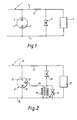
- the arrangement comprises a gas-filled voltage arrester 1 having a gas-filled enclosure in which are housed two electrodes 2, 3 which define between them a discharge gap. External leads are provided to each of the electrodes 2, 3, each lead being connected to a respective one of a pair of electrical supply lines 4, 5 extending between a load 7 to be protected and a supply (not shown). Also connected across the supply lines 4, 5 is a semiconductor arrester 9. A resistor 11 is connected in one of the supply lines 4 between the gas-filled excess voltage arrester 1 and semiconductor arrester 9, the semiconductor arrester being on the load side of the resistor 11.
- the first embodiment includes a gas-filled voltage arrester 21 comprising a gas-filled enclosure in which are housed two electrodes 22, 23 which define between them a discharge gap.
- An external lead is provided to each electrode 22, 23, the leads being connected to respective ones of a pair of lines 24, 25 extending between the load 27 to be protected and a supply (not shown).
- a semiconductor arrester 29 Also connected across the supply lines 24, 25 is a semiconductor arrester 29.
- a resistor 31 is connected in one of the supply lines 24 between the gas-filled excess voltage arrester 21 and semiconductor arrester 29, the arrester 29 being on the load side of the resistor 31.
- the circuit arrangement is the same as the known hybrid circuit arrangement described with reference to Figure 1.
- the circuit arrangement shown in Figure 2 is however distinguished from this known arrangement in that the primary winding 33 of a step up transformer is connected in series with the semiconductor arrester 29 between the supply lines 24, 25, a secondary winding of the transformer being connected between the supply line 25 and a trigger electrode 37 located within the enclosure of the gas-filled excess voltage arrester 21 ; via a limiting resistor 39.
- a further semiconductor arrester 41 is connected in parallel with the primary winding 33.
- the resulting current flowing through the primary winding 33 of the step up transformer causes a sufficiently high voltage to be applied between the trigger electrode 37 and the electrode 2 of the gas-filled excess voltage arrester 21 through the limiting resistor 39 to cause the arrester 21 to strike a discharge between the electrodes 37 and 23 followed by a sympathetic discharge between the electrodes 22 and 23.
- the majority of the current of the voltage surge will then flow between the electrodes 22 and 23, thus preventing the semiconductor arrester 29 from burning out.
- the semiconductor arrester 41 ensures that the inductive voltage drop across the primary winding 33 of the transformer can not exceed the breakdown voltage of the semiconductor arrester 41, even when the rate of rise of the incoming voltage surge is very high. Thus the voltage applied across the load 27 can not exceed the sum of the breakdown voltages of the two semiconductor arresters 29 and 41.
- the semiconductor arrester 29 is arranged to breakd ⁇ wn• at 50 volts, and a voltage of 500 volts then appears across the secondary winding 35 of the transformer which is applied through the limiting resistor 39 between the trigger electrode 37 and electrode 23 to cause the arrester 21 to fire if a voltage of 100 or more volts exists between electrodes 22 and 23.
- FIG. 3 shows an example of such a circuit arrangement.
- the arrangement includes a gas-filled voltage arrester 51 comprising a gas-filled enclosure in which are housed four electrodes 53, 55, 57, 59 .
- a respective external lead is provided to each of the electrodes, the electrodes 53 and 55 being connected via their respective leads to a respective one of a pair of lines 61, 63 extending between the load 65 to be protected and a supply (not shown).
- the electrode 57 is connected via its respective lead to an earth line 67, the fourth electrode 59 being a trigger electrode as further described hereafter.
- the electrodes 53, 55, 57 define three discharge gaps these being between line and line, and each of the lines 61, 63 and the earth line 67.
- a respective resistor 73 or 75 is connected in each of the supply lines61, 63 between the arrester 51 and the series arrangement of arresters 69, 71.
- the primary winding of a step-up transformer 77 is connected between the earth line 67 to the junction between the arresters 69, 71, a secondary winding of the transformer being connected in series with limiting resistor 79 between the trigger electrode 59 of the arrester 51 and earth.
- a further semiconductor arrester 81 is connected in parallel with the primary winding of the transformer 77.
- the arrangement operates in equivalent fashion to the arrangement described in relation to Figure 2.
- a sufficiently high voltage will then be applied between the trigger electrode 59 and the relevant electrode 53 or 55 to cause the arrester 51 to strike a discharge between the trigger electrode and the relevant electrode 53 or 57, thus being followed by a sympathetic discharge between the electrodes 53 and 55, or 53 and 57, or 55 and 57.
- the majority of the current of the voltage surge will flow in the gas-filled arrester, preventing the semiconductor arrester 69 ot 71 from burning out.
- the semiconductor arrester 81 ensures that voltage drop between either of the lines 61 and 63 and earth can not exceed the sum of the breakdown voltages of the two semiconductor arresters 69 and 81 or 71 and 81.
Landscapes
- Emergency Protection Circuit Devices (AREA)
Abstract
Description
- This invention relates to circuit arrangements. More particularly the invention relates to circuit arrangements for protecting a load connected across an electrical supply against surge voltages, the circuit arrangement incorporating a voltage arrester comprising a gas-filled enclosure housing a pair of electrodes which define between them a discharge gap. In use of such an arrangement the arrester is connected in parallel with the load across the electrical supply lines to the load or across one of the supply lines and an earth line, such that if a surge voltage greater than the breakdown voltage of the discharge gap appears on the supply, the arrester will strike a discharge, thus shortcircuiting the surge voltage and protecting the load.
- As gas-filled excess voltage arresters do not normally strike at voltages of less than about 300 volts, for the protection of, for example, integrated circuits which may be damaged by voltage spikes of only a few tens of volts , it is usual to use a so-called hybrid circuit arrangement, including a second voltage arrester, normally a semiconductor arrester, connected in parallel with the gas-filled voltage arrester, the second arrester being arranged to break down at a somewhat lower voltage than the gas-filled arrester.
- A problem arises, however, with known hybrid circuit arrangements where there is a sustained surge voltage which causes the semiconductor arrester to conduct, but is of insufficient magnitude to cause the voltage drop across the resistor and semiconductor arrester to reach the breakdown voltage of the discharge gap of the gas-filled arrester. The gas-filled arrester will then not strike a discharge, and the semiconductor arrester is likely to become overloaded and fail.
- It is an object of the present invention to provide a circuit arrangement for protecting a load connected across an electrical supply against surge voltages wherein this problem is alleviated.
- According to the invention a circuit arrangement for protecting a load connected across a supply against surge voltages comprises: a resistance connected in a line between the load and the supply; a first voltage arrester including a gas-filled enclosure housing two electrodes which define between them a discharge gap connected between said line on the supply side of said resistance and a further line between said load and said supply; a second excess voltage arrester of lower breakdown voltage than said discharge gap of said first arrester connected between said lines on the load side of said resistance, a trigger electrode within the enclosure of said first arrester; and firing means responsive to breakdown of said second arrester to apply a voltage between said trigger electrode and an electrode of said first arrester, thereby to reduce the breakdown voltage of said discharge gap of said first arrester.
- In order that the present invention may be more readily understood, a known circuit arrangement, and two embodiments of surge protection circuits according to the invention, will now be decribed by way of example and with reference to the accompanying drawings, in which
- Figure 1 is a circuit diagram of a known hybrid surge protection circuit arrangement,
- Figure 2 is a circuit diagram of a first embodiment of a hybrid surge protection circuit arrangement according to the invention, and
- Figure 3 is a similar diagram of a second embodiment.
- Referring to Figure 1, the arrangement comprises a gas-filled voltage arrester 1 having a gas-filled enclosure in which are housed two
electrodes electrodes electrical supply lines 4, 5 extending between a load 7 to be protected and a supply (not shown). Also connected across thesupply lines 4, 5 is a semiconductor arrester 9. Aresistor 11 is connected in one of the supply lines 4 between the gas-filled excess voltage arrester 1 and semiconductor arrester 9, the semiconductor arrester being on the load side of theresistor 11. - In operation, when a surge voltage appears between the
supply lines 4, 5 which causes the semiconductor arrester 9 to conduct, the total voltage drop across theresistor 11 and semiconductor arrester 9 is usually sufficient to exceed the breakdown voltage of the discharge gap between theelectrodes - Referring now to Figure 2, the first embodiment includes a gas-filled
voltage arrester 21 comprising a gas-filled enclosure in which are housed twoelectrodes electrode lines load 27 to be protected and a supply (not shown). Also connected across thesupply lines semiconductor arrester 29. Aresistor 31 is connected in one of thesupply lines 24 between the gas-filledexcess voltage arrester 21 andsemiconductor arrester 29, thearrester 29 being on the load side of theresistor 31. - As so far described, the circuit arrangement is the same as the known hybrid circuit arrangement described with reference to Figure 1. The circuit arrangement shown in Figure 2 is however distinguished from this known arrangement in that the
primary winding 33 of a step up transformer is connected in series with thesemiconductor arrester 29 between thesupply lines supply line 25 and atrigger electrode 37 located within the enclosure of the gas-filledexcess voltage arrester 21 ; via alimiting resistor 39. Afurther semiconductor arrester 41 is connected in parallel with theprimary winding 33. - In operation, when a voltage surge appears between the
lines semiconductor arrester 29 to conduct, but of insufficient magnitude to fire thearrester 21, the resulting current flowing through theprimary winding 33 of the step up transformer causes a sufficiently high voltage to be applied between thetrigger electrode 37 and theelectrode 2 of the gas-filledexcess voltage arrester 21 through the limitingresistor 39 to cause thearrester 21 to strike a discharge between theelectrodes electrodes electrodes semiconductor arrester 41 ensures that the inductive voltage drop across theprimary winding 33 of the transformer can not exceed the breakdown voltage of thesemiconductor arrester 41, even when the rate of rise of the incoming voltage surge is very high. Thus the voltage applied across theload 27 can not exceed the sum of the breakdown voltages of the twosemiconductor arresters - In a typical arrangement the
semiconductor arrester 29 is arranged to breakdδwn• at 50 volts, and a voltage of 500 volts then appears across thesecondary winding 35 of the transformer which is applied through the limitingresistor 39 between thetrigger electrode 37 andelectrode 23 to cause thearrester 21 to fire if a voltage of 100 or more volts exists betweenelectrodes - It will be appreciated that whilst the circuit arrangement described above by way of example uses a gas-filled voltage arrester having a single pair of main electrodes defining a discharge gap connected across a single pair of lines, in other arrangemnts in accordance with the invention a gas-filled arrester having two or more discharge gaps connected between respective pairs of supply lines may be used, a trigger electrode and firing means being provided to reduce the breakdown voltage of each such discharge gap.
- Figure 3 shows an example of such a circuit arrangement. Referring to this Figure, the arrangement includes a gas-filled
voltage arrester 51 comprising a gas-filled enclosure in which are housed fourelectrodes electrodes 53 and 55 being connected via their respective leads to a respective one of a pair oflines load 65 to be protected and a supply (not shown). Theelectrode 57 is connected via its respective lead to anearth line 67, thefourth electrode 59 being a trigger electrode as further described hereafter. - Thus the
electrodes lines earth line 67. - Also connected across the
supply lines semiconductor arresters respective resistor arrester 51 and the series arrangement ofarresters up transformer 77 is connected between theearth line 67 to the junction between thearresters resistor 79 between thetrigger electrode 59 of thearrester 51 and earth. Afurther semiconductor arrester 81, is connected in parallel with the primary winding of thetransformer 77. - The arrangement operates in equivalent fashion to the arrangement described in relation to Figure 2. Voltage surges appearing between
lines lines lines arrester electrodes transformer 77. A sufficiently high voltage will then be applied between thetrigger electrode 59 and therelevant electrode 53 or 55 to cause thearrester 51 to strike a discharge between the trigger electrode and therelevant electrode 53 or 57, thus being followed by a sympathetic discharge between theelectrodes ot 71 from burning out. Thesemiconductor arrester 81 ensures that voltage drop between either of thelines semiconductor arresters
Claims (7)
Applications Claiming Priority (4)
| Application Number | Priority Date | Filing Date | Title |
|---|---|---|---|
| GB8424907 | 1984-10-03 | ||
| GB848424907A GB8424907D0 (en) | 1984-10-03 | 1984-10-03 | Circuit arrangements |
| GB8510051 | 1985-04-19 | ||
| GB858510051A GB8510051D0 (en) | 1985-04-19 | 1985-04-19 | Circuit arrangements |
Publications (2)
| Publication Number | Publication Date |
|---|---|
| EP0186939A2 true EP0186939A2 (en) | 1986-07-09 |
| EP0186939A3 EP0186939A3 (en) | 1987-08-19 |
Family
ID=26288292
Family Applications (1)
| Application Number | Title | Priority Date | Filing Date |
|---|---|---|---|
| EP85307042A Withdrawn EP0186939A3 (en) | 1984-10-03 | 1985-10-02 | Circuit arrangements |
Country Status (3)
| Country | Link |
|---|---|
| US (1) | US4683514A (en) |
| EP (1) | EP0186939A3 (en) |
| GB (1) | GB2166307B (en) |
Cited By (9)
| Publication number | Priority date | Publication date | Assignee | Title |
|---|---|---|---|---|
| DE19838776A1 (en) * | 1998-08-26 | 2000-03-09 | Dehn & Soehne | Two-stage overvoltage protection method for low voltage plants, detects energy converted in second stage, and coarse protection stage is activated so that fine protection stage is relieved. |
| DE19952004A1 (en) * | 1999-08-17 | 2001-03-08 | Dehn & Soehne | Method for operating an overvoltage protection device and overvoltage protection device with at least one coarse protection and one fine protection element |
| DE10245144B3 (en) * | 2002-07-08 | 2004-01-22 | Dehn + Söhne Gmbh + Co. Kg | Surge protection arrangement with a spark gap as a coarse protection element |
| DE10004130B4 (en) * | 1998-08-26 | 2004-03-18 | Dehn + Söhne Gmbh + Co. Kg | Procedure for the safe operation of an at least two-stage surge protection device |
| CN100424958C (en) * | 2004-10-26 | 2008-10-08 | 曾献昌 | A, C, mains overvoltage protector having metalic ceramic gas discharge tube |
| WO2013019284A2 (en) * | 2011-07-29 | 2013-02-07 | Leviton Manufacturing Co., Inc. | Circuit interrupter with improved surge suppression |
| US9709626B2 (en) | 2008-01-29 | 2017-07-18 | Leviton Manufacturing Company, Inc. | Self testing fault circuit apparatus and method |
| US9759758B2 (en) | 2014-04-25 | 2017-09-12 | Leviton Manufacturing Co., Inc. | Ground fault detector |
| CN109075535A (en) * | 2016-02-18 | 2018-12-21 | 菲尼克斯电气公司 | A kind of overvoltage protection device |
Families Citing this family (28)
| Publication number | Priority date | Publication date | Assignee | Title |
|---|---|---|---|---|
| JPS6216929U (en) * | 1985-07-17 | 1987-01-31 | ||
| US4868505A (en) * | 1988-06-09 | 1989-09-19 | Stahl G J | High voltage impulse wave generator for testing equipment |
| US4918565A (en) * | 1988-08-11 | 1990-04-17 | King Larry J | Electrical surge suppressor |
| US5136455A (en) * | 1990-03-16 | 1992-08-04 | Esp Electronic Systems Protection, Inc. | Electromagnetic interference suppression device |
| GB9021222D0 (en) * | 1990-09-28 | 1990-11-14 | Raychem Ltd | Circuit protection device |
| JPH053667A (en) * | 1991-06-26 | 1993-01-08 | Toshiba Corp | Protective unit for thyristor circuit |
| AU714162B2 (en) * | 1994-11-29 | 1999-12-23 | Erico Lightning Technologies Pty Ltd | Ignition apparatus and method |
| DE19803636A1 (en) * | 1998-02-02 | 1999-08-05 | Phoenix Contact Gmbh & Co | Surge protection system |
| US6195245B1 (en) | 1998-05-29 | 2001-02-27 | Porta Systems Corp. | Low capacitance surge protector for high speed data transmission |
| EP1077519B1 (en) * | 1999-08-17 | 2005-10-26 | Dehn + Söhne Gmbh + Co Kg | Method of operating an overvoltage protection device and overvoltage protection device with at least one coarse and one fine protection element |
| DE10164232A1 (en) * | 2001-12-31 | 2003-07-17 | Phoenix Contact Gmbh & Co | Multipole surge protection system and method for the safe operation of a multipole surge protection system |
| CN1327586C (en) * | 2003-01-16 | 2007-07-18 | 黄兴英 | Surge protective method by self-control surge current triggered gap discharge |
| FR2864711B1 (en) * | 2003-12-30 | 2006-04-21 | Soule Protection Surtensions | OVERVOLTAGE PROTECTION DEVICE WITH SIMULTANEOUS TRIGGERED PARALLEL ECLATORS |
| US20090021881A1 (en) * | 2004-07-26 | 2009-01-22 | Vincent Andre Lucien Crevenat | Overvoltage protection device with improved leakage-current-interrupting capacity |
| FR2874287B1 (en) * | 2004-08-13 | 2006-10-27 | Soule Prot Surtensions Sa | DEVICE FOR PROTECTING ELECTRIC OVERVOLTAGE INSTALLATIONS HAVING AN ECLATOR ASSOCIATED WITH A PRE-RELEASE CIRCUIT |
| SE530248C2 (en) * | 2006-08-25 | 2008-04-08 | Powerwave Technologies Sweden | Active lightning protection |
| US7948726B2 (en) * | 2008-09-25 | 2011-05-24 | Panasonic Automotive Systems Company Of America, Division Of Panasonic Corporation Of North America | Electrostatic discharge (ESD) protection circuit and method |
| US8320094B2 (en) * | 2009-01-16 | 2012-11-27 | Circa Enterprises, Inc. | Surge protection module |
| KR101209275B1 (en) * | 2011-04-25 | 2012-12-10 | 한국전자통신연구원 | Surge protection apparatus and method using same |
| CZ25171U1 (en) | 2012-08-28 | 2013-04-04 | Saltek S.R.O. | Circuit arrangement of over-voltage protection firing circuit |
| CZ305207B6 (en) * | 2012-08-28 | 2015-06-10 | Saltek S.R.O. | Circuit arrangement of overvoltage protection firing circuit |
| DE102013108658B4 (en) * | 2013-08-09 | 2022-03-17 | Tdk Electronics Ag | Spark gap assembly and electronic component |
| WO2015089763A1 (en) * | 2013-12-18 | 2015-06-25 | Telefonaktiebolaget L M Ericsson (Publ) | Surge protection device and telecommunication equipment comprising the same |
| CZ305623B6 (en) * | 2014-01-03 | 2016-01-13 | Saltek S.R.O. | Circuit arrangement of overvoltage protection firing circuit with asymmetrical element |
| CZ26520U1 (en) | 2014-01-03 | 2014-02-24 | Saltek S.R.O. | Circuit arrangement of over-voltage protection circuit with asymmetric element |
| DE102015114504A1 (en) * | 2015-08-31 | 2017-03-02 | Epcos Ag | Mehrfachfunkenstreckenableiter |
| CN106159926B (en) * | 2016-06-29 | 2019-01-15 | 四川中光防雷科技股份有限公司 | A kind of surge protection circuit and Surge Protector |
| US20180337529A1 (en) * | 2017-05-16 | 2018-11-22 | Hamilton Sundstrand Corporation | Aerospace lightning protection for electrical devices |
Citations (2)
| Publication number | Priority date | Publication date | Assignee | Title |
|---|---|---|---|---|
| US3934175A (en) * | 1973-12-03 | 1976-01-20 | General Semiconductor Industries, Inc. | Power surge protection system |
| DE2537023A1 (en) * | 1975-03-17 | 1976-09-30 | Buckbee Mears Co | SURGE ARRESTERS |
Family Cites Families (9)
| Publication number | Priority date | Publication date | Assignee | Title |
|---|---|---|---|---|
| GB1080623A (en) * | 1964-07-14 | 1967-08-23 | English Electric Co Ltd | Improvements in or relating to protective spark gaps |
| US3480832A (en) * | 1966-11-14 | 1969-11-25 | Dale Electronics | Electrical surge arrestor |
| US3497764A (en) * | 1967-09-25 | 1970-02-24 | Gen Electric | Overvoltage protective apparatus having a pilot gap circuit arrangement for controlling its actuation |
| US3581264A (en) * | 1969-04-21 | 1971-05-25 | Dale Electronics | Method of creating variable electrical resistance and means for creating the same |
| GB1354245A (en) * | 1972-05-18 | 1974-06-05 | Gni Energet I Im Gm Krzhizhano | Electrical power surge arrestors |
| IT1016268B (en) * | 1974-07-02 | 1977-05-30 | Gni Energet In | EQUIPMENT FOR PROTECTING THE THYRISTORS OF A HIGH VOLTAGE CONTROLLED VERTITOR FROM OVER VOLTAGE |
| US4271445A (en) * | 1978-12-20 | 1981-06-02 | Bell Telephone Laboratories, Incorporated | Solid-state protector circuitry using gated diode switch |
| US4544983A (en) * | 1983-04-28 | 1985-10-01 | Northern Telecom Limited | Overvoltage protection device |
| US4586104A (en) * | 1983-12-12 | 1986-04-29 | Rit Research Corp. | Passive overvoltage protection devices, especially for protection of computer equipment connected to data lines |
-
1985
- 1985-10-01 US US06/782,434 patent/US4683514A/en not_active Expired - Fee Related
- 1985-10-02 GB GB08524320A patent/GB2166307B/en not_active Expired
- 1985-10-02 EP EP85307042A patent/EP0186939A3/en not_active Withdrawn
Patent Citations (2)
| Publication number | Priority date | Publication date | Assignee | Title |
|---|---|---|---|---|
| US3934175A (en) * | 1973-12-03 | 1976-01-20 | General Semiconductor Industries, Inc. | Power surge protection system |
| DE2537023A1 (en) * | 1975-03-17 | 1976-09-30 | Buckbee Mears Co | SURGE ARRESTERS |
Cited By (19)
| Publication number | Priority date | Publication date | Assignee | Title |
|---|---|---|---|---|
| DE19838776C2 (en) * | 1998-08-26 | 2002-01-10 | Dehn & Soehne | Method and arrangement with a two-stage surge protection in low-voltage systems |
| DE10004130B4 (en) * | 1998-08-26 | 2004-03-18 | Dehn + Söhne Gmbh + Co. Kg | Procedure for the safe operation of an at least two-stage surge protection device |
| DE19838776A1 (en) * | 1998-08-26 | 2000-03-09 | Dehn & Soehne | Two-stage overvoltage protection method for low voltage plants, detects energy converted in second stage, and coarse protection stage is activated so that fine protection stage is relieved. |
| DE19952004A1 (en) * | 1999-08-17 | 2001-03-08 | Dehn & Soehne | Method for operating an overvoltage protection device and overvoltage protection device with at least one coarse protection and one fine protection element |
| DE19952004B4 (en) * | 1999-08-17 | 2004-04-15 | Dehn + Söhne Gmbh + Co. Kg | Method for operating an overvoltage protection device and overvoltage protection device with at least one coarse protection and one fine protection element |
| DE10245144B3 (en) * | 2002-07-08 | 2004-01-22 | Dehn + Söhne Gmbh + Co. Kg | Surge protection arrangement with a spark gap as a coarse protection element |
| DE10245144C5 (en) * | 2002-07-08 | 2007-10-31 | Dehn + Söhne Gmbh + Co. Kg | Overvoltage protection arrangement with a spark gap as coarse protection element |
| CN100424958C (en) * | 2004-10-26 | 2008-10-08 | 曾献昌 | A, C, mains overvoltage protector having metalic ceramic gas discharge tube |
| US9709626B2 (en) | 2008-01-29 | 2017-07-18 | Leviton Manufacturing Company, Inc. | Self testing fault circuit apparatus and method |
| US11112453B2 (en) | 2008-01-29 | 2021-09-07 | Leviton Manufacturing Company, Inc. | Self testing fault circuit apparatus and method |
| US10656199B2 (en) | 2008-01-29 | 2020-05-19 | Leviton Manufacturing Company, Inc. | Self testing fault circuit apparatus and method |
| WO2013019284A2 (en) * | 2011-07-29 | 2013-02-07 | Leviton Manufacturing Co., Inc. | Circuit interrupter with improved surge suppression |
| US8599522B2 (en) | 2011-07-29 | 2013-12-03 | Leviton Manufacturing Co., Inc. | Circuit interrupter with improved surge suppression |
| WO2013019284A3 (en) * | 2011-07-29 | 2013-04-04 | Leviton Manufacturing Co., Inc. | Circuit interrupter with improved surge suppression |
| US9759758B2 (en) | 2014-04-25 | 2017-09-12 | Leviton Manufacturing Co., Inc. | Ground fault detector |
| US10401413B2 (en) | 2014-04-25 | 2019-09-03 | Leviton Manufacturing Company, Inc. | Ground fault detector |
| US10641812B2 (en) | 2014-04-25 | 2020-05-05 | Leviton Manufacturing Company, Inc. | Ground fault detector |
| CN109075535A (en) * | 2016-02-18 | 2018-12-21 | 菲尼克斯电气公司 | A kind of overvoltage protection device |
| CN109075535B (en) * | 2016-02-18 | 2020-04-14 | 菲尼克斯电气公司 | Overvoltage protection equipment |
Also Published As
| Publication number | Publication date |
|---|---|
| GB2166307A (en) | 1986-04-30 |
| GB8524320D0 (en) | 1985-11-06 |
| GB2166307B (en) | 1987-11-25 |
| US4683514A (en) | 1987-07-28 |
| EP0186939A3 (en) | 1987-08-19 |
Similar Documents
| Publication | Publication Date | Title |
|---|---|---|
| EP0186939A2 (en) | Circuit arrangements | |
| EP0204723B1 (en) | Auto-reset circuit breaker | |
| US5440441A (en) | Apparatus for protecting, monitoring, and managing an AC/DC electrical line or a telecommunication line using a microprocessor | |
| US4174530A (en) | Voltage surge arrester device | |
| JPS6217454B2 (en) | ||
| US7755873B2 (en) | Device for protection against voltage surges with parallel simultaneously triggered spark-gaps | |
| US4860156A (en) | Overvoltage protective circuit | |
| US20090021881A1 (en) | Overvoltage protection device with improved leakage-current-interrupting capacity | |
| US5883775A (en) | Overvoltage protector | |
| KR100845224B1 (en) | Overvoltage protective device and method of overvoltage protection | |
| EP0061838B1 (en) | Surge voltage protection arrangements | |
| US20050063118A1 (en) | Multipole overvoltage protection system and method for the reliable operation of a multipole overvoltage protection system | |
| EP0162228B1 (en) | Interactive overvoltage protection device | |
| EP0050966B1 (en) | Protection circuit for a power distribution system | |
| EP0123126A1 (en) | Overvoltage protection device | |
| SE440574B (en) | OVER MONEY PROTECTION | |
| JPH0145812B2 (en) | ||
| US3149263A (en) | Electric overvoltage arrester with large capacitive spark gap | |
| WO1987000984A1 (en) | Surge voltage protection arrangements | |
| US4340921A (en) | HVDC Power transmission system with metallic return conductor | |
| JPH0729712Y2 (en) | Surge protector | |
| GB1585041A (en) | Over-voltage protection circuits | |
| US3544847A (en) | Flip-flop lightning arrester with reduced protective level | |
| KR102582296B1 (en) | Surge protection apparatus for LED | |
| US3911322A (en) | Method and circuit arrangement for an improved low cost lightning arrester |
Legal Events
| Date | Code | Title | Description |
|---|---|---|---|
| PUAI | Public reference made under article 153(3) epc to a published international application that has entered the european phase |
Free format text: ORIGINAL CODE: 0009012 |
|
| AK | Designated contracting states |
Kind code of ref document: A2 Designated state(s): DE FR |
|
| 17P | Request for examination filed |
Effective date: 19861031 |
|
| PUAL | Search report despatched |
Free format text: ORIGINAL CODE: 0009013 |
|
| RHK1 | Main classification (correction) |
Ipc: H02H 9/06 |
|
| AK | Designated contracting states |
Kind code of ref document: A3 Designated state(s): DE FR |
|
| STAA | Information on the status of an ep patent application or granted ep patent |
Free format text: STATUS: THE APPLICATION IS DEEMED TO BE WITHDRAWN |
|
| 18D | Application deemed to be withdrawn |
Effective date: 19880220 |
|
| RIN1 | Information on inventor provided before grant (corrected) |
Inventor name: COOK, KENNETH GEORGE |