EP0186667B1 - Montierung von halbleiterchips - Google Patents
Montierung von halbleiterchips Download PDFInfo
- Publication number
- EP0186667B1 EP0186667B1 EP85902088A EP85902088A EP0186667B1 EP 0186667 B1 EP0186667 B1 EP 0186667B1 EP 85902088 A EP85902088 A EP 85902088A EP 85902088 A EP85902088 A EP 85902088A EP 0186667 B1 EP0186667 B1 EP 0186667B1
- Authority
- EP
- European Patent Office
- Prior art keywords
- mount
- recess
- thermal
- board
- semi
- Prior art date
- Legal status (The legal status is an assumption and is not a legal conclusion. Google has not performed a legal analysis and makes no representation as to the accuracy of the status listed.)
- Expired
Links
- 239000004065 semiconductor Substances 0.000 title claims abstract description 14
- 239000012815 thermoplastic material Substances 0.000 claims abstract description 10
- 239000004020 conductor Substances 0.000 claims abstract description 7
- 238000001465 metallisation Methods 0.000 claims description 3
- 239000004697 Polyetherimide Substances 0.000 claims description 2
- 229920000265 Polyparaphenylene Polymers 0.000 claims description 2
- UCKMPCXJQFINFW-UHFFFAOYSA-N Sulphide Chemical compound [S-2] UCKMPCXJQFINFW-UHFFFAOYSA-N 0.000 claims description 2
- 229920006258 high performance thermoplastic Polymers 0.000 claims description 2
- 229920002492 poly(sulfone) Polymers 0.000 claims description 2
- 229920001601 polyetherimide Polymers 0.000 claims description 2
- -1 polyphenylene Polymers 0.000 claims description 2
- 230000000593 degrading effect Effects 0.000 abstract description 2
- 229920001169 thermoplastic Polymers 0.000 abstract description 2
- 239000004416 thermosoftening plastic Substances 0.000 abstract description 2
- 239000011810 insulating material Substances 0.000 description 3
- 239000000463 material Substances 0.000 description 3
- 239000003822 epoxy resin Substances 0.000 description 2
- 238000000034 method Methods 0.000 description 2
- 229920000647 polyepoxide Polymers 0.000 description 2
- 230000004308 accommodation Effects 0.000 description 1
- 239000000853 adhesive Substances 0.000 description 1
- 230000001070 adhesive effect Effects 0.000 description 1
- 239000000969 carrier Substances 0.000 description 1
- 230000015556 catabolic process Effects 0.000 description 1
- 239000000919 ceramic Substances 0.000 description 1
- 229910010293 ceramic material Inorganic materials 0.000 description 1
- 239000011248 coating agent Substances 0.000 description 1
- 238000000576 coating method Methods 0.000 description 1
- 239000002131 composite material Substances 0.000 description 1
- 150000001875 compounds Chemical class 0.000 description 1
- 230000007547 defect Effects 0.000 description 1
- 238000006731 degradation reaction Methods 0.000 description 1
- 238000001746 injection moulding Methods 0.000 description 1
- 239000002184 metal Substances 0.000 description 1
- 238000000465 moulding Methods 0.000 description 1
- 238000013021 overheating Methods 0.000 description 1
- 238000012856 packing Methods 0.000 description 1
- 238000004382 potting Methods 0.000 description 1
- 239000000758 substrate Substances 0.000 description 1
Images
Classifications
-
- H—ELECTRICITY
- H01—ELECTRIC ELEMENTS
- H01L—SEMICONDUCTOR DEVICES NOT COVERED BY CLASS H10
- H01L23/00—Details of semiconductor or other solid state devices
- H01L23/12—Mountings, e.g. non-detachable insulating substrates
-
- H—ELECTRICITY
- H05—ELECTRIC TECHNIQUES NOT OTHERWISE PROVIDED FOR
- H05K—PRINTED CIRCUITS; CASINGS OR CONSTRUCTIONAL DETAILS OF ELECTRIC APPARATUS; MANUFACTURE OF ASSEMBLAGES OF ELECTRICAL COMPONENTS
- H05K1/00—Printed circuits
- H05K1/18—Printed circuits structurally associated with non-printed electric components
- H05K1/182—Printed circuits structurally associated with non-printed electric components associated with components mounted in the printed circuit board, e.g. insert mounted components [IMC]
- H05K1/183—Components mounted in and supported by recessed areas of the printed circuit board
-
- H—ELECTRICITY
- H01—ELECTRIC ELEMENTS
- H01L—SEMICONDUCTOR DEVICES NOT COVERED BY CLASS H10
- H01L23/00—Details of semiconductor or other solid state devices
- H01L23/12—Mountings, e.g. non-detachable insulating substrates
- H01L23/14—Mountings, e.g. non-detachable insulating substrates characterised by the material or its electrical properties
- H01L23/145—Organic substrates, e.g. plastic
-
- H—ELECTRICITY
- H01—ELECTRIC ELEMENTS
- H01L—SEMICONDUCTOR DEVICES NOT COVERED BY CLASS H10
- H01L23/00—Details of semiconductor or other solid state devices
- H01L23/52—Arrangements for conducting electric current within the device in operation from one component to another, i.e. interconnections, e.g. wires, lead frames
- H01L23/538—Arrangements for conducting electric current within the device in operation from one component to another, i.e. interconnections, e.g. wires, lead frames the interconnection structure between a plurality of semiconductor chips being formed on, or in, insulating substrates
- H01L23/5384—Conductive vias through the substrate with or without pins, e.g. buried coaxial conductors
-
- H—ELECTRICITY
- H01—ELECTRIC ELEMENTS
- H01L—SEMICONDUCTOR DEVICES NOT COVERED BY CLASS H10
- H01L2924/00—Indexing scheme for arrangements or methods for connecting or disconnecting semiconductor or solid-state bodies as covered by H01L24/00
- H01L2924/0001—Technical content checked by a classifier
- H01L2924/0002—Not covered by any one of groups H01L24/00, H01L24/00 and H01L2224/00
-
- H—ELECTRICITY
- H05—ELECTRIC TECHNIQUES NOT OTHERWISE PROVIDED FOR
- H05K—PRINTED CIRCUITS; CASINGS OR CONSTRUCTIONAL DETAILS OF ELECTRIC APPARATUS; MANUFACTURE OF ASSEMBLAGES OF ELECTRICAL COMPONENTS
- H05K1/00—Printed circuits
- H05K1/02—Details
- H05K1/0201—Thermal arrangements, e.g. for cooling, heating or preventing overheating
- H05K1/0203—Cooling of mounted components
- H05K1/0204—Cooling of mounted components using means for thermal conduction connection in the thickness direction of the substrate
- H05K1/0206—Cooling of mounted components using means for thermal conduction connection in the thickness direction of the substrate by printed thermal vias
-
- H—ELECTRICITY
- H05—ELECTRIC TECHNIQUES NOT OTHERWISE PROVIDED FOR
- H05K—PRINTED CIRCUITS; CASINGS OR CONSTRUCTIONAL DETAILS OF ELECTRIC APPARATUS; MANUFACTURE OF ASSEMBLAGES OF ELECTRICAL COMPONENTS
- H05K2201/00—Indexing scheme relating to printed circuits covered by H05K1/00
- H05K2201/09—Shape and layout
- H05K2201/09009—Substrate related
- H05K2201/09036—Recesses or grooves in insulating substrate
-
- H—ELECTRICITY
- H05—ELECTRIC TECHNIQUES NOT OTHERWISE PROVIDED FOR
- H05K—PRINTED CIRCUITS; CASINGS OR CONSTRUCTIONAL DETAILS OF ELECTRIC APPARATUS; MANUFACTURE OF ASSEMBLAGES OF ELECTRICAL COMPONENTS
- H05K2201/00—Indexing scheme relating to printed circuits covered by H05K1/00
- H05K2201/09—Shape and layout
- H05K2201/09209—Shape and layout details of conductors
- H05K2201/09372—Pads and lands
- H05K2201/09472—Recessed pad for surface mounting; Recessed electrode of component
Definitions
- This invention relates to mounting semi-conductor chips, such as integrated circuit dies or discrete components on an electronic circuit mount such as a circuit or wiring board to form an electronic sub-assembly.
- Conventional printed circuit boards are formed of a thin board (of between 0.0127 mm and 32 mm thickness) with a conducting interconnected pattern formed on one or both faces of the board; feedthroughs and vias being provided to connect the interconnection patterns on either face of the board and for wires or leads from discrete components, semi-conductor chips and integrated circuit dies that are often mounted on carriers which are then added to complete the circuit for the thus formed sub-assembly.
- Printed circuits have also been produced with several alternating layers of metal film and insulating film mounted on a single board; boards with up to 32 layers of interconnections have been produced. Such multilayer boards have enhanced components/chips/ die packing densities and reduced interconnection lengths resulting in higher operating speeds for the sub-assembly.
- United Kingdom Patent Specification No. 953503 (Telefunken) describes the mounting of an active circuit element in a recess at one side of a carrier plate of insulating material, the only insulating material disclosed being ceramic material.
- United Kingdom Patent Specification No. 2026234A (Mitsumi) also describes the accommodation of a circuit element chip within a concavity or depression in a ceramicsubstrate, the use of substrate materials otherthan ceramic is contraindicated by the disclosure of this specification (see page 1 lines 31 to 34).
- thermoplastic material It is an object of the present invention to provide an electronic circuit mount having recesses to house semi-conductor chips and being easily moulded, inexpensive and, for high frequency operations, having improved dielectric characteristics. This can be achieved by moulding from thermoplastic material.
- thermoplastic material is its ease of thermal degradation and it is a further object of the present invention to overcome this defect.
- an electronic circuit mount for semi-conductor chips, has a series of closed-bottomed recesses within the thickness of the mount, with each recess opening to a surface of the mount and being shaped to house a semi-conductor chip of given configuration; the mount having an applied pattern of chip-interconnecting electrical conductors extending over the mount and to each recess; the mount being moulded from thermoplastic material and each recess having means for conducting away and dissipating heat therefrom.
- the heat conducting and dissipating means convey heat generated by a chip away from the recess it is mounted in and prevents the thermoplastic of the mount in the area of the recess from degrading.
- the heat conducting and dissipating means comprise one or more thermal vias extending from each recess to another surface of the mount.
- the heat conducting and dissipating means further comprise an applied thermal conducting layer extending over part of each recess, the or each thermal via and a part of said other surface of the mount.
- the mount is a circuit board
- the recesses each open to one of the opposed faces of the board
- the thermal vias extend from the bottom of each recess to the opposite board face
- the thermal conducting layer extends over the bottom of each recess.
- the pattern of electrical conductors and the thermal conducting layer are simultaneously applied to the mount by a process of selective metalisation.
- a cover for each recess may be provided in the form of a lid moulded from thermoplastic material and shaped to fit the sides of the recess and to be flush with the mount surface.
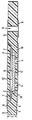
- a board 1 has a recess 2 in one face 3 thereof; as shown the recess is within the thickness of the board (in an example the thickness is 1.6 mm).
- Thermal vias or holes 4 are provided in the bottom of the recess 2, which vias emerge on the opposite face 5 of the board.
- the board is provided with an applied pattern 6 of chip-interconnecting electrical conductors that covers face 3 of the board and extends down into the recess 2 to provide wiring connection points 7 for the electrical connection of wiring-leads 8 to a semi-conductor chip 9, such as an integrated circuit die that is housed in the recess.
- the bottom of the recess, the thermal vias 4 and a part of the opposite face 5 of the board are covered with a thermal conducting layer 10 the chip 9 being bonded, such as by a thermally conductive adhesive, to the layer in the recess bottom.
- the thermal vias 4 and conducting layer 10 serve to conduct heat from the semi-conductor chip 9 to the thermal coating on the other side of the board which forms a spreader plane to radiate the heat generated in the semi-conductor device.
- Feedthroughsforthe board 1 are provided in the form of vias 11 from one to the other sides of the board through which vias the conducting pattern 6 can extend.
- the recess 2 is covered by a lid 12 that is shaped to fit the sides of the recess and be essentially flush with the surface of the board face 3. Additionally, the remaining free space 13 within the recess can be filled with an insulating material, such as an epoxy resin to "pot" the chip in the device both to anchor it therein and provide additional protection beyond that provided by the lip 12.
- an insulating material such as an epoxy resin to "pot" the chip in the device both to anchor it therein and provide additional protection beyond that provided by the lip 12.
- the board may be formed using high performance thermoplastic materials either filled or unfilled of the type polyethyersulphone, polysulphone, polyetherimide, polyphenylene sulphide or the like and may be produced by injection moulding or any other suitable technique.
- the electrical conducting interconnection pattern 6 is then produced on the board sides and into the recess by selective metallisation.
- the thermal conducting layer 10 is also formed by selective metallisation, preferably by the same operation as that forming the electrical conducting pattern 6.
- the lid 12 can be similarly formed and from similar materials and is adhesively bonded or welded into place, after filling any free space within the recess with an epoxy resin potting compound.
- More than one recess is provided on each board to mount further semi-conductor chips or devices and further chips or devices may be surface mounted or through hole mounted on to the board to provide a complete electronic sub-assembly that can be functionally tested before further assembly.
- the composite structure of the thus formed electronic sub-assembly will operate at much higher speeds than conventionally packaged and interconnected systems due to the short interconnection lengths possible and the low dielectric constant of the materials used; whilst the thermal conduction means prevents the board from overheating in the area of each recess, to the detriment of both the chip and the board thermoplastic material.
Landscapes
- Engineering & Computer Science (AREA)
- Microelectronics & Electronic Packaging (AREA)
- Physics & Mathematics (AREA)
- Condensed Matter Physics & Semiconductors (AREA)
- General Physics & Mathematics (AREA)
- Computer Hardware Design (AREA)
- Power Engineering (AREA)
- Magnetic Heads (AREA)
- Structures For Mounting Electric Components On Printed Circuit Boards (AREA)
- Photoreceptors In Electrophotography (AREA)
- Die Bonding (AREA)
- Dry Shavers And Clippers (AREA)
- Mechanical Treatment Of Semiconductor (AREA)
- Structure Of Printed Boards (AREA)
- Structures Or Materials For Encapsulating Or Coating Semiconductor Devices Or Solid State Devices (AREA)
- Cooling Or The Like Of Semiconductors Or Solid State Devices (AREA)
Claims (9)
Priority Applications (1)
| Application Number | Priority Date | Filing Date | Title |
|---|---|---|---|
| AT85902088T ATE34881T1 (de) | 1984-05-24 | 1985-05-09 | Montierung von halbleiterchips. |
Applications Claiming Priority (2)
| Application Number | Priority Date | Filing Date | Title |
|---|---|---|---|
| GB8413330 | 1984-05-24 | ||
| GB848413330A GB8413330D0 (en) | 1984-05-24 | 1984-05-24 | Mounting semi-conductor chips |
Publications (2)
| Publication Number | Publication Date |
|---|---|
| EP0186667A1 EP0186667A1 (de) | 1986-07-09 |
| EP0186667B1 true EP0186667B1 (de) | 1988-06-01 |
Family
ID=10561466
Family Applications (1)
| Application Number | Title | Priority Date | Filing Date |
|---|---|---|---|
| EP85902088A Expired EP0186667B1 (de) | 1984-05-24 | 1985-05-09 | Montierung von halbleiterchips |
Country Status (8)
| Country | Link |
|---|---|
| EP (1) | EP0186667B1 (de) |
| JP (1) | JPS61502226A (de) |
| KR (1) | KR860700183A (de) |
| AT (1) | ATE34881T1 (de) |
| DE (1) | DE3563150D1 (de) |
| DK (1) | DK24486A (de) |
| GB (1) | GB8413330D0 (de) |
| WO (1) | WO1985005496A1 (de) |
Families Citing this family (11)
| Publication number | Priority date | Publication date | Assignee | Title |
|---|---|---|---|---|
| DE3843787A1 (de) * | 1988-12-24 | 1990-07-05 | Standard Elektrik Lorenz Ag | Verfahren und leiterplatte zum montieren eines halbleiter-bauelements |
| US5241456A (en) * | 1990-07-02 | 1993-08-31 | General Electric Company | Compact high density interconnect structure |
| KR0134902B1 (ko) * | 1991-07-08 | 1998-04-20 | 다니엘 케이. 니콜스 | 칩 캐리어 패키지 및 집적 회로 패키지 |
| AUPR244901A0 (en) * | 2001-01-10 | 2001-02-01 | Silverbrook Research Pty Ltd | A method (WSM02) |
| AUPR245501A0 (en) | 2001-01-10 | 2001-02-01 | Silverbrook Research Pty Ltd | An apparatus (WSM08) |
| AU2004202251B2 (en) * | 2001-01-10 | 2004-07-08 | Silverbrook Research Pty Ltd | Wafer scale molding of protective caps |
| AU2004214607B2 (en) * | 2001-01-10 | 2005-11-03 | Silverbrook Research Pty Ltd | An integrated circuit assembly incorporating protective caps |
| AU2002218870B2 (en) * | 2001-01-10 | 2004-03-04 | Silverbrook Research Pty Ltd | Molds for wafer scale molding of protective caps |
| AU2004202411B2 (en) * | 2001-01-10 | 2005-11-10 | Silverbrook Research Pty Ltd | An apparatus for fabricating packaged semiconductor devices |
| US7652895B2 (en) * | 2002-04-11 | 2010-01-26 | Tpo Displays Corp. | Electrically insulating body, and electronic device |
| FI20040592A (fi) * | 2004-04-27 | 2005-10-28 | Imbera Electronics Oy | Lämmön johtaminen upotetusta komponentista |
Family Cites Families (4)
| Publication number | Priority date | Publication date | Assignee | Title |
|---|---|---|---|---|
| US3777220A (en) * | 1972-06-30 | 1973-12-04 | Ibm | Circuit panel and method of construction |
| DE2546443C3 (de) * | 1975-10-16 | 1979-04-05 | Siemens Ag, 1000 Berlin Und 8000 Muenchen | Zusammengesetzte Mikroschaltung und Verfahren zu ihrer Herstellung |
| US4396936A (en) * | 1980-12-29 | 1983-08-02 | Honeywell Information Systems, Inc. | Integrated circuit chip package with improved cooling means |
| US4472876A (en) * | 1981-08-13 | 1984-09-25 | Minnesota Mining And Manufacturing Company | Area-bonding tape |
-
1984
- 1984-05-24 GB GB848413330A patent/GB8413330D0/en active Pending
-
1985
- 1985-05-09 AT AT85902088T patent/ATE34881T1/de not_active IP Right Cessation
- 1985-05-09 EP EP85902088A patent/EP0186667B1/de not_active Expired
- 1985-05-09 JP JP60502126A patent/JPS61502226A/ja active Pending
- 1985-05-09 WO PCT/GB1985/000196 patent/WO1985005496A1/en active IP Right Grant
- 1985-05-09 DE DE8585902088T patent/DE3563150D1/de not_active Expired
-
1986
- 1986-01-16 KR KR860700026A patent/KR860700183A/ko not_active Application Discontinuation
- 1986-01-17 DK DK24486A patent/DK24486A/da not_active Application Discontinuation
Also Published As
| Publication number | Publication date |
|---|---|
| WO1985005496A1 (en) | 1985-12-05 |
| DK24486D0 (da) | 1986-01-17 |
| JPS61502226A (ja) | 1986-10-02 |
| KR860700183A (ko) | 1986-03-31 |
| ATE34881T1 (de) | 1988-06-15 |
| DE3563150D1 (en) | 1988-07-07 |
| GB8413330D0 (en) | 1984-06-27 |
| DK24486A (da) | 1986-01-17 |
| EP0186667A1 (de) | 1986-07-09 |
Similar Documents
| Publication | Publication Date | Title |
|---|---|---|
| KR960000711B1 (ko) | 반도체장치 및 그 제조방법 | |
| US10892231B2 (en) | Electronics package including integrated electromagnetic interference shield and method of manufacturing thereof | |
| US5599747A (en) | Method of making circuitized substrate | |
| US6029343A (en) | Insulated surface mount circuit board construction | |
| US5583378A (en) | Ball grid array integrated circuit package with thermal conductor | |
| US6449168B1 (en) | Circuit board and a method for manufacturing the same | |
| US6396141B2 (en) | Tape ball grid array with interconnected ground plane | |
| EP0004148A1 (de) | Elektrisches Verbindungsstück zur Montage einer elektronischen Vorrichtung auf ein Substrat | |
| JP2660295B2 (ja) | 電子部品搭載用基板 | |
| US4819041A (en) | Surface mounted integrated circuit chip package and method for making same | |
| US5869889A (en) | Thin power tape ball grid array package | |
| US6323065B1 (en) | Methods for manufacturing ball grid array assembly semiconductor packages | |
| EP0186667B1 (de) | Montierung von halbleiterchips | |
| US20090133904A1 (en) | Module and manufacturing method thereof | |
| US6221694B1 (en) | Method of making a circuitized substrate with an aperture | |
| US5041943A (en) | Hermetically sealed printed circuit board | |
| US5966803A (en) | Ball grid array having no through holes or via interconnections | |
| US6207354B1 (en) | Method of making an organic chip carrier package | |
| US20020063331A1 (en) | Film carrier semiconductor device | |
| US6057594A (en) | High power dissipating tape ball grid array package | |
| JPS6344745A (ja) | 電子部品搭載用基板 | |
| JPH041738Y2 (de) | ||
| JP3648252B2 (ja) | 熱伝導特性を有する表面実装型パッケージ | |
| KR19980044540A (ko) | 클립 리드 패키지 | |
| JPS6134989A (ja) | 電子部品搭載用基板 |
Legal Events
| Date | Code | Title | Description |
|---|---|---|---|
| PUAI | Public reference made under article 153(3) epc to a published international application that has entered the european phase |
Free format text: ORIGINAL CODE: 0009012 |
|
| 17P | Request for examination filed |
Effective date: 19860114 |
|
| AK | Designated contracting states |
Kind code of ref document: A1 Designated state(s): AT BE CH DE FR GB IT LI LU NL SE |
|
| 17Q | First examination report despatched |
Effective date: 19870803 |
|
| GRAA | (expected) grant |
Free format text: ORIGINAL CODE: 0009210 |
|
| AK | Designated contracting states |
Kind code of ref document: B1 Designated state(s): AT BE CH DE FR GB IT LI LU NL SE |
|
| REF | Corresponds to: |
Ref document number: 34881 Country of ref document: AT Date of ref document: 19880615 Kind code of ref document: T |
|
| ITF | It: translation for a ep patent filed | ||
| REF | Corresponds to: |
Ref document number: 3563150 Country of ref document: DE Date of ref document: 19880707 |
|
| ET | Fr: translation filed | ||
| PLBE | No opposition filed within time limit |
Free format text: ORIGINAL CODE: 0009261 |
|
| STAA | Information on the status of an ep patent application or granted ep patent |
Free format text: STATUS: NO OPPOSITION FILED WITHIN TIME LIMIT |
|
| 26N | No opposition filed | ||
| PG25 | Lapsed in a contracting state [announced via postgrant information from national office to epo] |
Ref country code: LU Free format text: LAPSE BECAUSE OF NON-PAYMENT OF DUE FEES Effective date: 19890531 |
|
| PGFP | Annual fee paid to national office [announced via postgrant information from national office to epo] |
Ref country code: SE Payment date: 19900329 Year of fee payment: 6 Ref country code: CH Payment date: 19900329 Year of fee payment: 6 |
|
| PGFP | Annual fee paid to national office [announced via postgrant information from national office to epo] |
Ref country code: FR Payment date: 19900330 Year of fee payment: 6 |
|
| PGFP | Annual fee paid to national office [announced via postgrant information from national office to epo] |
Ref country code: GB Payment date: 19900424 Year of fee payment: 6 |
|
| PGFP | Annual fee paid to national office [announced via postgrant information from national office to epo] |
Ref country code: LU Payment date: 19900425 Year of fee payment: 6 |
|
| PGFP | Annual fee paid to national office [announced via postgrant information from national office to epo] |
Ref country code: BE Payment date: 19900515 Year of fee payment: 6 |
|
| PGFP | Annual fee paid to national office [announced via postgrant information from national office to epo] |
Ref country code: AT Payment date: 19900518 Year of fee payment: 6 |
|
| ITTA | It: last paid annual fee | ||
| PGFP | Annual fee paid to national office [announced via postgrant information from national office to epo] |
Ref country code: NL Payment date: 19900531 Year of fee payment: 6 |
|
| PGFP | Annual fee paid to national office [announced via postgrant information from national office to epo] |
Ref country code: DE Payment date: 19900626 Year of fee payment: 6 |
|
| PG25 | Lapsed in a contracting state [announced via postgrant information from national office to epo] |
Ref country code: GB Effective date: 19910509 Ref country code: AT Effective date: 19910509 |
|
| PG25 | Lapsed in a contracting state [announced via postgrant information from national office to epo] |
Ref country code: SE Effective date: 19910510 |
|
| PG25 | Lapsed in a contracting state [announced via postgrant information from national office to epo] |
Ref country code: LI Effective date: 19910531 Ref country code: CH Effective date: 19910531 Ref country code: BE Effective date: 19910531 |
|
| BERE | Be: lapsed |
Owner name: MBM TECHNOLOGY LTD Effective date: 19910531 |
|
| PG25 | Lapsed in a contracting state [announced via postgrant information from national office to epo] |
Ref country code: NL Effective date: 19911201 |
|
| GBPC | Gb: european patent ceased through non-payment of renewal fee | ||
| NLV4 | Nl: lapsed or anulled due to non-payment of the annual fee | ||
| PG25 | Lapsed in a contracting state [announced via postgrant information from national office to epo] |
Ref country code: FR Effective date: 19920131 |
|
| REG | Reference to a national code |
Ref country code: CH Ref legal event code: PL |
|
| PG25 | Lapsed in a contracting state [announced via postgrant information from national office to epo] |
Ref country code: DE Effective date: 19920303 |
|
| REG | Reference to a national code |
Ref country code: FR Ref legal event code: ST |
|
| EUG | Se: european patent has lapsed |
Ref document number: 85902088.5 Effective date: 19911209 |