EP0186401A2 - Einstellbares Widerstandsnetzwerk - Google Patents
Einstellbares Widerstandsnetzwerk Download PDFInfo
- Publication number
- EP0186401A2 EP0186401A2 EP85309122A EP85309122A EP0186401A2 EP 0186401 A2 EP0186401 A2 EP 0186401A2 EP 85309122 A EP85309122 A EP 85309122A EP 85309122 A EP85309122 A EP 85309122A EP 0186401 A2 EP0186401 A2 EP 0186401A2
- Authority
- EP
- European Patent Office
- Prior art keywords
- current
- current source
- transistor
- providing
- effective resistance
- Prior art date
- Legal status (The legal status is an assumption and is not a legal conclusion. Google has not performed a legal analysis and makes no representation as to the accuracy of the status listed.)
- Granted
Links
Images
Classifications
-
- H—ELECTRICITY
- H03—ELECTRONIC CIRCUITRY
- H03H—IMPEDANCE NETWORKS, e.g. RESONANT CIRCUITS; RESONATORS
- H03H11/00—Networks using active elements
- H03H11/46—One-port networks
Definitions
- Resistors are basic components of most electronic circuits. They are used for biasing, current limiting and a wide range of functions determined by the resistance of the resistor and the particular circuit in which they are used.
- Filters are one type of circuit employing resistors that are used extensively in the field of electrical signal processing. Fundamentally, the filter has a capacitor and a resistor whose values define the frequency response of the filter. Thus, a different value for either the capacitor or the resistor will result in a change in the frequency response.
- the frequency response has been changed by substituting a capacitor of one value for a capacitor of another value or by changing a resistor of one value for a resistor of another value. Therefore, a given filter may not be easily used in two different applications requiring different frequency responses since it may be necessary to change either the capacitor or resistor, so that the filter may be usable in either application. Moreover, if
- the filter is implemented as an integrated circuit, it would not be possible to change the capacitor or resistor.
- phase-locked loop One application of a filter involves its use in a circuit known as a phase-locked loop.
- One overall function of a phase-locked loop is to receive an input signal and then output a frequency signal in dependence on any difference in phase between the input signal and the output signal.
- the phase-locked loop includes a phase detector which receives the input signal and the output signal to generate a phase error signal, the filter that filters the phase error signal and a voltage controlled oscillator that responds to the filtered phase error signal to output and feed back to the phase detector the output frequency signal.
- the filter will have a frequency response that is predetermined based on the data rate of the input signal that the phase-locked loop is processing.
- phase-locked loop particularly one being implemented as an integrated circuit
- inflexibility in being able to be used with different input signals having different data rates. This stems in part from the use of the filter and its fixed frequency response based on the set capacitor and resistor values of the filter.
- the value of resistance of a resistor may have important effects on the operation of circuits employing the resistor.
- apparatus having a controllable effective resistance
- the apparatus comprising a transistor means for providing a current at an input node responsive to an input voltage at the input node, coupled to a settable current source.
- the settable current source operates to control the effective value of the controllable effective resistance.
- filtering apparatus comprising a filter which has a controllable filter response and includes a charge storage device, and an apparatus having a controllable effective resistance coupled to the charge storage device.
- the filter apparatus also includes a means for controlling the controllable effective resistance to set the filter response.
- apparatus providing an output frequency signal in response to an input signal having a nominal data rate
- the apparatus comprising phase-locked loop means for generating the output signal in response to a difference in phase between the output frequency signal and the input signal, including a controllable filter having a frequency response in dependence on the nominal data rate of the input signal, and means for controlling the controllable filter to have the frequency response.
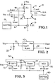
- F ig. 1 shows a schematic diagram of an apparatus 10 having a controllable effective resistance.
- the apparatus 10 includes a transistor means 11 for providing a current I OUT that is proportional to an input voltage V IN supplied at the input node 12 for small input voltages.
- a settable current source 13 is coupled to the transistor means 11.
- the settable current source 13 supplies variable current in response to a reference signal generated by a control means 19.
- By varying the settable current source 13, the magnitude of the current I OUT is varied, thereby providing a controllable effective voltage to current conversion.
- the apparatus 10 behaves essentially as a resistor with controllable resistance.
- the transistor means 11 in the embodiment of Fig. 1 includes a differential pair of transistors 14, 15.
- the base of transistor 14 is coupled to the input node 12 across resistor Rl. Also the base of transistor 14 is coupled to a reference voltage V REF across resistor R2.
- the base of transistor 15 is coupled to the reference voltage V REF across resistor R3.
- the settable current source 13' includes a first variable current source 16 and a second variable current source 17.
- the first variable current source 16 supplies a current 2I C which is twice the current I e of the second variable current source 17.
- the second variable current source 17 supplies a balanc - ing current to the apparatus 10 so that it can behave as a classical resistor as discussed below, and can be varied or eliminated in some applications.
- the emitters of the differential pair of transistors 14, 15 are coupled to the first variable current source 16.
- the collector of one transistor 14 of the differential pair of transistors 14, 15 is coupled to the second variable current source 17.
- controllable effective resistance 10 shown in Fig. 1 supplies a current on line 18 which is proportional to the voltage difference between the input voltage V IN and the reference voltage V REF for small values of V IN .
- the output current I OUT on line 18 is zero. This is so because the second variable current source 17 supplies current I e through the collector of the one transistor 14 which satisfies the balance condition of the differential pair 14, 15. So I OUT must be zero. The other transistor 15 will conduct an equal current I e through its collector to satisfy the second variable current source 16.
- the effective resistance of the apparatus 10 having a controllable effective resistance of Fig. 1 can be calculated in simplified form.
- the effective resistance R EFF is determined by the following equation (1):
- the output current IOUT on line 18 is derived by the following equation (2): where F is equal to a constant for small values of (V IN - V REF ) determined by the characteristics of the differential pair of transistors 14, 15.
- the apparatus 10 has a controllable effective resistance that is controllable in response to the settable current source 13.
- the effective resistance R EFF of the apparatus 10 is likewise controlled.
- the settable current source 13 receives a reference signal on a control line 21 from a control means 19 for controlling the settable current source 13.
- the control means 19 may include current mirrors or other current scaling apparatus which provide a reference signal on line 21 for controlling the settable current source 13.
- the operation of the control means 19 to generate the reference signal on control line 21 can be varied in accordance with the particular application of the apparatus 10. For instance, for apparatus 10 having a controllable effective resistance employed in a RC filter, the control means 19 may supply a reference signal on control line 21 which is proportional to the desired breakpoint frequency f B of the RC filter. Other relationships between the control means 19 and the apparatus 10 will be determined by the particular application of the apparatus 10 having a controllable effective resistance.
- Fig. 2 is a block diagram of a filter apparatus 20 employing the apparatus 10 having a controllable effective resistance.
- the filter apparatus 20 includes a charge storage means for storing charge, such as capacitor C, coupled across the input node 12 of the apparatus 10 to a ground terminal.
- the apparatus 10 provides an output current I OUT which is proportional to the voltage ( VIN - V REF ).
- the value of the controllable effective resistance is determined by the reference signal on line 21 which controls the setting of the settable current source 13.
- the filter apparatus 20 provides a filter having a settable frequency response because of the manner in which the controllable effective resistance of apparatus 10 is employed. The following simplified equations prove the relationship.
- the breakpoint frequency f of the filter apparatus 20 is given by the following equation (4):
- the control signal on line 21 is of a character for controlling the settable current source 13 of the controllable effective resistance 10.
- the settable current source 13 can be manufactured in a variety of embodiments including digital or analog versions which are responsive to a control signal.
- the reference signal is generated in response to the desired breakpoint frequency f B , and the settable current source 13 is scaled to provide a current which results in the desired effective resistance R EFF for the given capacitance of the charge storage device C.
- the filter apparatus 20 in the preferred embodiment is formed on a semiconductor wafer in an integrated circuit. Because of the inability to vary charge storage devices in integrated circuits easily, the filter apparatus 20 employing the apparatus 10 having a controllable effective resistance has particular utility.
- Fig. 3 illustrates a block diagram of a phase-locked loop apparatus 30 employing the apparatus 10 having a controllable effective resistance.
- the phase-locked loop apparatus 30 includes a phase detector 31, a filter apparatus 20, and a voltage controlled oscillator 32.
- the phase detector 31 compares a difference in phase between an input signal V IN having a given frequency, or nominal data rate, with the output frequency signal V OUT from the voltage control oscillator 32 having a settable frequency.
- the output of the phase detector 31 is a signal proportional to the difference in phase between V IN and V OUT .
- the output of the phase detector 31 is filtered by the controllable filter apparatus 20 and supplied as input to the voltage controlled oscillator 32.
- the frequency of the voltage Controlled oscillator is shifted in response to the output from the controllable filter apparatus 20 in order to track the input signal V IN '
- the voltage controlled oscillator 32 operates at a center frequency in response to a reference signal I REF on line 33.
- the filter apparatus 20 and the phase detector 31 are set to operate with a breakpoint frequency f B that is proportional to the frequency of operation of the voltage controlled oscillator 32.
- the reference signal I REF on line 33, the reference signal I REF on line 21 for controlling the effective resistance of the controllable effective resistance 20, and the reference signal I REF on line 50 for centering the phase detector 31 are generated in conjunction in control means 40 for generating the reference signal in dependence on the nominal data rate of V IN to provide a phase-locked loop apparatus 30 which operates over a wide range of center frequencies.
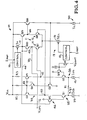
- Fig. 4 illustrates a circuit diagram of a preferred embodiment for the present invention for implementation on an integrated circuit chip.
- the reference numbers from Fig. 1 are used in Fig. 4 where appropriate for consistency.
- the transistor means 11 is comprised of a differential pair of transistors 14, 15.
- Transistor Q7 corresponds to the one transistor 14 of Fig. 1 and transistor Q8 corresponds to the other transistor 15 of Fig. 1.
- the settable current source 13 is comprised of a first variable current source 16 and a second variable current source 17.
- the first variable current source 16 supplies 2I C current at the emitters of the differential pair of transistors Q7, Q8.
- the first variable current source 16 and second variable current source 17 are set to a desired current level by control 19.
- the control 19 is implemented with settable current mirrors or other control circuitry as suits the user.
- the second variable current source 17 supplier current through the diode means Q10 to the collector of the one transistor Q7.
- the output current I OUT is supplied over line 18 from the collector of transistor Q7 to the input node 12.
- the apparatus 10 having a controllable effective resistance of the embodiment shown in Fig. 4 provides an effective resistance REFF across a differential input voltage ( V LEFT - V RIGHT ).
- a means 35 for providing overall temperature compensation is provided. Also, a means 36 for maintaining appropriate bias voltages at the bases of the differential pair of transistors Q7, Q8 is provided.
- the means 35 for providing temperature compensation includes a first current path 37 and a second current path 38.
- the first current path 37 includes a current source 39 supplying current to the emitter of a transistor Q1.
- the collector of the transistor Q1 is connected to a node 40 which is connected to the base of the transistor Q8 of the transistor means 11.
- Another transistor Q3 is connected at its emitter to the node 40.
- the collector of the transistor Q3 is connected through resistor R2 to the supply voltage V CC .
- the second current path 38 likewise includes a current source 41 supplying current to the emitter of a transistor Q2.
- the collector of the transistor Q2 is connected to a' node 42 which is coupled to the base of the transistor Q7 of the transistor means 11.
- Another transistor Q4 is coupled at its emitter to the node 42.
- the collector of transistor Q4 is coupled across resistor R3 to the reference voltage V CC'
- the emitters of the transistor Ql of the first current path 37 and Q2 of the second current path 38 are coupled together across resistor Rl.
- the base of the transistor Q1 of the first current path 37 is coupled to the voltage V LEFT at input node 12 across the emitter follower transistor Q12 over line 46 across diode means Q10.
- the base of transistor Q2 of the second currant path 38 is coupled to the voltage V RIGHT across the emitter follower Q13 and diode means Q14 which matches diode means Q10.
- the voltage node 42 follows the voltage VLEFT at node 12. Likewise, the voltage at node 40 follows the voltage V RIGHT . This occurs because the differential voltage V LEFT - VRIGHT will cause a current to flow across the resistor R1.
- V LEFT is at a higher voltage than V RIGHT
- the current through transistor Q2 will be less than the current through transistor Q1.
- the current sources 39, 41 draw equal current, a current must flow through R1 to the emitter of Q2 to balance the current.
- the voltage drop from the base to emitter of transistor Q4 will be less than the voltage drop from the base to emitter of transistor Q3.
- the voltage at node 42 will be higher than the voltage at node 40.
- Temperature compensation is provided by manufacturing transistor Q3 and Q4 to match transistors Q7 and Q8 of the transistor means 11 as closely as possible. Because a change in temperature will effect transistors Q3 and Q4 the same way as it will effect transistors Q7 and Q8, the voltages at nodes 40 and 42 applied to the bases of the differential pair of transistors Q7, Q8 will track the changes in the impedance of the base to emitter junction of the transistors Q7 and Q8 as the temperature changes.
- the range of bias voltages available is limited due to low supply voltages.
- the present apparatus overcomes that limitation by including the means 36 for providing bias voltages.
- the means 36 for providing bias voltages for the transistor means 11 includes transistors Q5, Q6, Q9, Q10 and Qll. In order to maintain the transistor means 11 in its desired operating range without saturating the transistors in the ; means 35 for providing temperature compensation, the means 36 provides bias voltages to the transistor means 11 within the constraints of the integrated circuit environment.
- the means 36 comprises a voltage path as follows.
- the voltage at node 45 at the collector of the one transistor Q7 and the voltage at node 44 at the collector of the other transistor Q8 are held roughly equivalent through the diode connected transistor Q10 and down through the emitter of transistor Q9, which is connected to the node 44.
- the node at the emitter of the transistor Q6 is 1V BE below the voltage at the node 44.
- the voltage drop at the emitter of the transistor Q6 is made to track the voltage drops through the emitters of the transistors Q10 and Q9 by the controllable current source 90, which is controlled to deliver a current which is equal to about I c .
- the voltage at the emitter of the transistor Q6 is supplied to the base of the pnp transistor Q5.
- the voltage at the emitter of the transistor Q5 is thus approximately equal to the voltage at the node 44.
- the diode connected transistor Qll maintains the voltage at the node 43 approximately. 1VBE above the voltage at the node 44 and at the node 45.
- This circuit path assures that the voltage at the nodes 40 and 42 at the bases of the one transistor Q7 and the other transistor Q8 of the differential pair of transistors are maintained within an acceptable range of the voltages of the collectors of the one transistor Q7 and the other transistor Q8.
- the circuit shown in Fig. 4 illustrates a further feature of the preferred embodiment in that a means 46 for minimizing base current linkage through the apparatus 10 having a controllable effective resistance is provided.
- the means 46 is embodied by the emitter follower transistors Q12 and Q13 which provide additional gain at the input of the means 35 for providing temperature compensation.
- R EFF effective resistance
- the current flowing through the base of the temperature compensation circuit transistors Ql and Q 2 becomes significant. Accordingly, the emitter follower transistors Q12 and Q13 are provided to minimize the base current linkage while providing sufficient drive for the apparatus 10 having a controllable effective resistance.
- variable current sources including the first variable current source 16, the second variable current source 17 and the variable current source 90 in the circuit shown in Fig. 4 are preferably implemented by current mirrors that are adapted to provide a current that is a multiple of the reference signal I REF .
- the current mirrors are scaled in the control 19 to provide the correct multiples of the reference current I RE p.
- the reference signal, IREF which is used to center the VCO can be scaled in the control 19 to provide proper currents for the controllable effective resistance 10.
- the reference signal I REF will change accordingly.
- the effective value of the controllable effective resistance 10 will also change so that the bandwidth of the filter 20 in the phase-locked loop apparatus 30 will automatically adjust to the center frequency of the VCO 32.
- an apparatus 10 having a controllable effective resistance with a wide range of applications.
- the apparatus 10 can be used in the filter apparatus 20 : to provide a filter having a controllable frequency response over a wide range.
- a phase-locked loop apparatus which is operable over a wide range of frequency.
- the controllable effective resistance is controllable by varying a settable current source 13.
- the controllable effective resistance can be controlled to dynamically change the effective resistance R EFF of the apparatus in response to electronic signals.
Landscapes
- Networks Using Active Elements (AREA)
- Secondary Cells (AREA)
- Polymers With Sulfur, Phosphorus Or Metals In The Main Chain (AREA)
- Control Of Amplification And Gain Control (AREA)
Priority Applications (1)
| Application Number | Priority Date | Filing Date | Title |
|---|---|---|---|
| AT85309122T ATE76543T1 (de) | 1984-12-17 | 1985-12-16 | Einstellbares widerstandsnetzwerk. |
Applications Claiming Priority (2)
| Application Number | Priority Date | Filing Date | Title |
|---|---|---|---|
| US682384 | 1984-12-17 | ||
| US06/682,384 US4608543A (en) | 1984-12-17 | 1984-12-17 | Controllable effective resistance and phase lock loop with controllable filter |
Publications (3)
| Publication Number | Publication Date |
|---|---|
| EP0186401A2 true EP0186401A2 (de) | 1986-07-02 |
| EP0186401A3 EP0186401A3 (en) | 1988-01-27 |
| EP0186401B1 EP0186401B1 (de) | 1992-05-20 |
Family
ID=24739463
Family Applications (1)
| Application Number | Title | Priority Date | Filing Date |
|---|---|---|---|
| EP85309122A Expired EP0186401B1 (de) | 1984-12-17 | 1985-12-16 | Einstellbares Widerstandsnetzwerk |
Country Status (5)
| Country | Link |
|---|---|
| US (1) | US4608543A (de) |
| EP (1) | EP0186401B1 (de) |
| JP (1) | JPS61145920A (de) |
| AT (1) | ATE76543T1 (de) |
| DE (1) | DE3586096D1 (de) |
Cited By (2)
| Publication number | Priority date | Publication date | Assignee | Title |
|---|---|---|---|---|
| EP0621688A3 (de) * | 1993-04-19 | 1995-12-27 | Sanyo Electric Co | Schaltung mit hoher Impedanz. |
| US11963286B2 (en) | 2017-12-01 | 2024-04-16 | Excillum Ab | X-ray source and method for generating X-ray radiation |
Families Citing this family (3)
| Publication number | Priority date | Publication date | Assignee | Title |
|---|---|---|---|---|
| US4806888A (en) * | 1986-04-14 | 1989-02-21 | Harris Corp. | Monolithic vector modulator/complex weight using all-pass network |
| US4878028A (en) * | 1987-02-12 | 1989-10-31 | Advanced Micro Devices, Inc. | Technique for generating precompensation delay for writing data to disks |
| US6054903A (en) * | 1997-11-13 | 2000-04-25 | Lsi Logic Corporation | Dual-loop PLL with adaptive time constant reduction on first loop |
Family Cites Families (10)
| Publication number | Priority date | Publication date | Assignee | Title |
|---|---|---|---|---|
| AT303203B (de) * | 1970-11-12 | 1972-11-10 | Akg Akustische Kino Geraete | Schaltungsanordnung zur stufenlosen Pegeleinstellung elektrischer Signale |
| US3965441A (en) * | 1975-06-20 | 1976-06-22 | Trw Inc. | Parallel resonant circuit with feedback means for increasing Q |
| GB1573616A (en) * | 1976-03-04 | 1980-08-28 | Nat Semiconductor Uk Ltd | Electronic impedance devices |
| JPS5949728B2 (ja) * | 1976-12-27 | 1984-12-04 | 株式会社日立製作所 | 可変インピ−ダンス回路 |
| JPS5564420A (en) * | 1978-11-09 | 1980-05-15 | Toshiba Corp | Variable impedance circuit |
| JPS5738012A (en) * | 1980-08-20 | 1982-03-02 | Hitachi Ltd | Variable resistor circuit using current miller circuit |
| JPS6228086Y2 (de) * | 1980-12-08 | 1987-07-18 | ||
| JPS5836014A (ja) * | 1981-08-28 | 1983-03-02 | Hitachi Ltd | 電子インピ−ダンス装置 |
| JPS58120314A (ja) * | 1982-01-12 | 1983-07-18 | Toshiba Corp | 可変インピ−ダンス回路 |
| US4506233A (en) * | 1982-06-28 | 1985-03-19 | General Electric Company | Bandwidth control circuit for a phase locked loop |
-
1984
- 1984-12-17 US US06/682,384 patent/US4608543A/en not_active Expired - Lifetime
-
1985
- 1985-12-16 EP EP85309122A patent/EP0186401B1/de not_active Expired
- 1985-12-16 AT AT85309122T patent/ATE76543T1/de not_active IP Right Cessation
- 1985-12-16 DE DE8585309122T patent/DE3586096D1/de not_active Expired - Lifetime
- 1985-12-16 JP JP60284178A patent/JPS61145920A/ja active Pending
Cited By (3)
| Publication number | Priority date | Publication date | Assignee | Title |
|---|---|---|---|---|
| EP0621688A3 (de) * | 1993-04-19 | 1995-12-27 | Sanyo Electric Co | Schaltung mit hoher Impedanz. |
| US5757232A (en) * | 1993-04-19 | 1998-05-26 | Sanyo Electric Co. | High-impedance circuit having reduced stray capacitance |
| US11963286B2 (en) | 2017-12-01 | 2024-04-16 | Excillum Ab | X-ray source and method for generating X-ray radiation |
Also Published As
| Publication number | Publication date |
|---|---|
| EP0186401B1 (de) | 1992-05-20 |
| ATE76543T1 (de) | 1992-06-15 |
| US4608543A (en) | 1986-08-26 |
| EP0186401A3 (en) | 1988-01-27 |
| DE3586096D1 (de) | 1992-06-25 |
| JPS61145920A (ja) | 1986-07-03 |
Similar Documents
| Publication | Publication Date | Title |
|---|---|---|
| EP1111493B1 (de) | Spannungsregler mit kleiner Verlustspannung und niedrigem Ruhestrom | |
| US4792748A (en) | Two-terminal temperature-compensated current source circuit | |
| US4350904A (en) | Current source with modified temperature coefficient | |
| US4779037A (en) | Dual input low dropout voltage regulator | |
| US4349778A (en) | Band-gap voltage reference having an improved current mirror circuit | |
| US4506208A (en) | Reference voltage producing circuit | |
| US4435678A (en) | Low voltage precision current source | |
| US4524318A (en) | Band gap voltage reference circuit | |
| US4399398A (en) | Voltage reference circuit with feedback circuit | |
| US4348633A (en) | Bandgap voltage regulator having low output impedance and wide bandwidth | |
| US5315231A (en) | Symmetrical bipolar bias current source with high power supply rejection ratio (PSRR) | |
| EP0124918B1 (de) | Stromquellenanordnung | |
| US3546564A (en) | Stabilized constant current apparatus | |
| US5532579A (en) | Temperature stabilized low reference voltage generator | |
| US4590419A (en) | Circuit for generating a temperature-stabilized reference voltage | |
| US4608543A (en) | Controllable effective resistance and phase lock loop with controllable filter | |
| US4157493A (en) | Delta VBE generator circuit | |
| WO1997024650A1 (en) | Temperature stabilized constant fraction voltage controlled current source | |
| US3536986A (en) | Low level costant current source | |
| US6188268B1 (en) | Low side current sink circuit having improved output impedance to reduce effects of leakage current | |
| EP0080620B1 (de) | Spannungsregelschaltung mit verbotener Zone | |
| GB2226664A (en) | Shunt voltage regulator | |
| US5396193A (en) | Frequency response-compensated circuit | |
| US4280090A (en) | Temperature compensated bipolar reference voltage circuit | |
| HK85491A (en) | Current-discrimination arangement |
Legal Events
| Date | Code | Title | Description |
|---|---|---|---|
| PUAI | Public reference made under article 153(3) epc to a published international application that has entered the european phase |
Free format text: ORIGINAL CODE: 0009012 |
|
| AK | Designated contracting states |
Kind code of ref document: A2 Designated state(s): AT BE CH DE FR GB IT LI LU NL SE |
|
| PUAL | Search report despatched |
Free format text: ORIGINAL CODE: 0009013 |
|
| RHK1 | Main classification (correction) |
Ipc: H03H 11/46 |
|
| AK | Designated contracting states |
Kind code of ref document: A3 Designated state(s): AT BE CH DE FR GB IT LI LU NL SE |
|
| 17P | Request for examination filed |
Effective date: 19880201 |
|
| 17Q | First examination report despatched |
Effective date: 19900606 |
|
| GRAA | (expected) grant |
Free format text: ORIGINAL CODE: 0009210 |
|
| AK | Designated contracting states |
Kind code of ref document: B1 Designated state(s): AT BE CH DE FR GB IT LI LU NL SE |
|
| PG25 | Lapsed in a contracting state [announced via postgrant information from national office to epo] |
Ref country code: SE Effective date: 19920520 Ref country code: NL Effective date: 19920520 Ref country code: LI Effective date: 19920520 Ref country code: IT Free format text: LAPSE BECAUSE OF FAILURE TO SUBMIT A TRANSLATION OF THE DESCRIPTION OR TO PAY THE FEE WITHIN THE PRESCRIBED TIME-LIMIT;WARNING: LAPSES OF ITALIAN PATENTS WITH EFFECTIVE DATE BEFORE 2007 MAY HAVE OCCURRED AT ANY TIME BEFORE 2007. THE CORRECT EFFECTIVE DATE MAY BE DIFFERENT FROM THE ONE RECORDED. Effective date: 19920520 Ref country code: CH Effective date: 19920520 Ref country code: BE Effective date: 19920520 Ref country code: AT Effective date: 19920520 |
|
| REF | Corresponds to: |
Ref document number: 76543 Country of ref document: AT Date of ref document: 19920615 Kind code of ref document: T |
|
| REF | Corresponds to: |
Ref document number: 3586096 Country of ref document: DE Date of ref document: 19920625 |
|
| REG | Reference to a national code |
Ref country code: CH Ref legal event code: PL |
|
| ET | Fr: translation filed | ||
| NLV1 | Nl: lapsed or annulled due to failure to fulfill the requirements of art. 29p and 29m of the patents act | ||
| PG25 | Lapsed in a contracting state [announced via postgrant information from national office to epo] |
Ref country code: LU Free format text: LAPSE BECAUSE OF NON-PAYMENT OF DUE FEES Effective date: 19921231 |
|
| PLBE | No opposition filed within time limit |
Free format text: ORIGINAL CODE: 0009261 |
|
| STAA | Information on the status of an ep patent application or granted ep patent |
Free format text: STATUS: NO OPPOSITION FILED WITHIN TIME LIMIT |
|
| 26N | No opposition filed | ||
| PG25 | Lapsed in a contracting state [announced via postgrant information from national office to epo] |
Ref country code: DE Effective date: 19930901 |
|
| PGFP | Annual fee paid to national office [announced via postgrant information from national office to epo] |
Ref country code: GB Payment date: 20001107 Year of fee payment: 16 |
|
| PGFP | Annual fee paid to national office [announced via postgrant information from national office to epo] |
Ref country code: FR Payment date: 20001204 Year of fee payment: 16 |
|
| PG25 | Lapsed in a contracting state [announced via postgrant information from national office to epo] |
Ref country code: GB Free format text: LAPSE BECAUSE OF NON-PAYMENT OF DUE FEES Effective date: 20011216 |
|
| REG | Reference to a national code |
Ref country code: GB Ref legal event code: IF02 |
|
| GBPC | Gb: european patent ceased through non-payment of renewal fee |
Effective date: 20011216 |
|
| PG25 | Lapsed in a contracting state [announced via postgrant information from national office to epo] |
Ref country code: FR Free format text: LAPSE BECAUSE OF NON-PAYMENT OF DUE FEES Effective date: 20020830 |
|
| REG | Reference to a national code |
Ref country code: FR Ref legal event code: ST |