EP0184857A2 - Génération de couleurs multiples sur un dispositif d'affichage - Google Patents
Génération de couleurs multiples sur un dispositif d'affichage Download PDFInfo
- Publication number
- EP0184857A2 EP0184857A2 EP85115932A EP85115932A EP0184857A2 EP 0184857 A2 EP0184857 A2 EP 0184857A2 EP 85115932 A EP85115932 A EP 85115932A EP 85115932 A EP85115932 A EP 85115932A EP 0184857 A2 EP0184857 A2 EP 0184857A2
- Authority
- EP
- European Patent Office
- Prior art keywords
- color
- bit
- signals
- memory means
- bit map
- Prior art date
- Legal status (The legal status is an assumption and is not a legal conclusion. Google has not performed a legal analysis and makes no representation as to the accuracy of the status listed.)
- Withdrawn
Links
Images


Classifications
-
- G—PHYSICS
- G06—COMPUTING; CALCULATING OR COUNTING
- G06F—ELECTRIC DIGITAL DATA PROCESSING
- G06F3/00—Input arrangements for transferring data to be processed into a form capable of being handled by the computer; Output arrangements for transferring data from processing unit to output unit, e.g. interface arrangements
- G06F3/14—Digital output to display device ; Cooperation and interconnection of the display device with other functional units
- G06F3/153—Digital output to display device ; Cooperation and interconnection of the display device with other functional units using cathode-ray tubes
-
- G—PHYSICS
- G09—EDUCATION; CRYPTOGRAPHY; DISPLAY; ADVERTISING; SEALS
- G09G—ARRANGEMENTS OR CIRCUITS FOR CONTROL OF INDICATING DEVICES USING STATIC MEANS TO PRESENT VARIABLE INFORMATION
- G09G5/00—Control arrangements or circuits for visual indicators common to cathode-ray tube indicators and other visual indicators
- G09G5/02—Control arrangements or circuits for visual indicators common to cathode-ray tube indicators and other visual indicators characterised by the way in which colour is displayed
- G09G5/022—Control arrangements or circuits for visual indicators common to cathode-ray tube indicators and other visual indicators characterised by the way in which colour is displayed using memory planes
Definitions
- This invention relates generally to a graphics display in a data processing system, and more particularly to the automatic generation of different colors and shades of colors to fill out areas of the display.
- Graphics and alphanumeric text are displayed visually in many business applications. This allows the relationship between many variables of the business to be presented in pie chart or bar graph form.
- the graphics may also be used to display and manipulate mechanical or electronic designs in color.
- adjacent areas may be filled using different colors for adjacent areas.
- Prior art systems use a number of techniques for displaying color.
- One technique uses multiple memory planes for storage of codes representing different colors and shades. This approach requires a large amount of memory with its associated control logic.
- a second approach uses an analog display tube whereby varying signal levels represented by coded information stored in multiple planes of memory. This method requires large amounts of memory plus analog circuitry to drive a more expensive display tube.
- a third approach uses software to mix the colors by having coded information stored in main memory for each desired color. These codes are used to do paints to bit mapped memories by overlaying different colored patterns to obtain desired colors. This software approach provides additional overhead for the operating system thereby requiring additional memory and also reducing the throughput of the system.
- a color display graphics system includes three bit map memories for storing bits representing red, green and blue colors respectively. Combinations of bits from the same address locations of each bit map memory display a pixel which could be any one of eight colors: black, blue, green, cyan, red, magenta, yellow or white.
- a read only memory stores patterns made up of 16 bits in a four-by-four matrix for each of the red, green and blue colors.
- the 16-bit matrices are stored in their respective bit map memories for subsequent color display.
- a matrix may have 4, 8, 12 or 16 bits at binary ONE to display a 25%, 50%, 75% or 100% of a specific color. Also, two 25 % matrices may each be arranged in a pattern that they may be combined without overlap. One of the 25% matrices may be combined with a 75% matrix to display a color on all 16 pixels of the display. One of the 25% matrices may be combined with a 50% matrix without overlap.
- Combinations of matrices may be used to show shades of the above colors by combining white or black with the remaining colors or to show combinations of the other six colors.
- the graphics system operates in one of three modes of operation, .a REPLACE, an OR or an EXCLUSIVE OR mode of operation.
- the REPLACE mode of operation replaces the color pattern previously written into the area
- the OR mode of operation superimposes a selected color pattern on the existing color pattern
- the EXCLUSIVE OR mode of operation superimposes the selected color pattern on the displayed color pattern except that a color bit stored at an address of a bit map memory is erased if the new color bit is written into that addressed position resulting in a binary ZERO in that position.
- Logic couples the ROM to the bit map memories. Two bits for each color bit which indicate the mode of operation and binary state of the color bit are combined with an addressed bit from the respective bit map memory in accordance with the mode of operation to generate the new color bits to be written into their respective bit map memories.
- Figure 1 shows an overall block diagram of a display subsystem for displaying graphics in color on a display 40, typically a cathode ray tube (CRT) display.
- a display 40 typically a cathode ray tube (CRT) display.
- CRT cathode ray tube
- Address information is received by the graphics display subsystem from a personal computer option (PCO) interface address bus 2.
- Data information is received from a PCO interface data bus 36 and control information is received., from a PCO interface control bus 42.
- the PCO interface may receive information from a typical personal computer (not shown) or any typical data processing system (not shown).
- the graphics display is aimed at the business graphics marketplace wherein the ability to generate and modify color pie charts, line charts and the like is a requirement.
- Bit map memory 10-G stores bits which represent a green image on the display 40
- bit map memory 10-R stores bits which represent a red image on the display 40
- bit map memory 10-B stores bits which represent a blue image on the display 40.
- the bit map memories 10-G, 10-R and 10-B are addressed via an address multiplexer (MUX) 6 from either the PCO interface address bus 2 or the row and column address (RAS/CAS) counter 4.
- the address signals from the PCO interface address bus 2 may be used to update portions of the display with data received from the PCO interface data bus 36.
- the address signals from the RAS/CAS counter 4 may be used to sequentially read out the bits from the bit map memories 10-G, 10-R. and 10-B for display on display 40. Note that eight possible colors are possible by using combinations of the same address location in each of the bit map memories 10-G, 10-R and 10-B for displaying a pixel.
- a cycle control 12 which receives control signals from PCO interface control bus 42 controls the operation of the address MUX 6 and the RAS/CAS counter 4 to read bytes from bit map memories 10-G, 10-R and 10-B; A buffers 14-G, 14-R and 14-B; B buffers 16-G, 16-R and 16-B; and shift registers 18-G, 18-R and 18-B, respectively.
- a bit from each bit map memory 10-G, 10-R and 10-B representative of a pixel addresses a text mix read only memory (ROM) 22.
- the output signals of ROM 22 are applied to an output register 24 for transfer to display 40 for displaying the color pixel.
- Address signals from PCO interface address bus 2 are also applied to a pattern ROM 28 which provides signals to bit map memories 10-G, 10-R and 10-B to provide shades of the eight basic colors for the display in defined areas.
- a mode and output register 30 provides signals to define the mode of operation, either a REPLACE mode, an OR mode or an EXCLUSIVE OR mode.
- Bit select multiplexers (MUX) 20-G, 20-R and 20-B each select a bit from the byte read from the bit map memories 10-G, 10-R and 10-B, respectively, for storage in a bit register 32.
- the bit register output signals are applied to a read modify write 26.
- the read modify write 26 also receives the data bits from the pattern ROM 26 and performs the specified operation as indicated by the contents of mode control register 30 and writes the output of a read modify write 26 into the bit map memories 10-G, 10-R and 10-B.
- Figure 2 shows the detailed logic which updates the bit map memories 10-R, 10-G and 10-B.
- a ROM 28-1 stores bit patterns for updating bit map memory 10-R and ROM 28-2 stores bit patterns for updating bit map memories 10-G and 10-B.
- Each of the bit map memories 10-R, 10-G and 10-B controls their respective colors red, green and blue.
- combinations of red, green and blue as shown by the color octal numbers make up the five other colors black, cyan, magenta, yellow and white.
- octal 2 green (binary 010) with octal 4 red (binary 100) gives octal 6 yellow (binary 110).
- the logic of Figure 2 operates in one of three modes of operation as defined by mode signals BMODOO+00 and BMOD01+00.
- Signals BMODOO+00 and BMOD01+00 at logical ZERO define a REPLACE operation.
- REPLACE mode of operation a pixel stored in the bit map memories 10-R, 10-G and 10-B is replaced by the addressed bit pattern stored in ROM 28-1 and ROM 28-2 which represents the new pixel.
- a pixel represents a bit position on the display 40 made up of combinations of the three basic colors red, blue and green.
- Signal BMODOO+00 at logical ZERO and signal BMOD01+00 at logical ONE define an OR mode of operation.
- the new pixel displayed on the display 40 is made up of the bit pattern representing the new pixel superimposed on the old pixel.
- the OR operation allows the changing of the color of an area of display 40 by adding an appropriate bit to the bit map memories 10-G, 10-R and/or 10-B.
- Signal BMODOO+00 at logical ONE and signal BMOD01+00 at logical ZERO define an EXCLUSIVE OR mode of operation.
- the EXCLUSIVE OR mode allows the setting of a pixel to a binary ONE only if the stored pixel and the selected pattern pixel are different -- one equal to a binary ONE and the other equal to a binary ZERO. If the stored and selected pixels are equal, either both binary ZERO or both binary ONE, the resulting stored pixel will be a binary ZERO. This action will facilitate the erasing of a pixel pattern if the identical pixel pattern is written a second time.
- the EXCLUSIVE OR operation allows the changing of the color of an area by removing or adding appropriate bits from the bit map memories 10-G, 10-R and/or 10-B.
- signals PROMR1+00, PROMG1+00 and PROMB1+00 are at logical ZERO.
- Signals PROMRO+00, PROMGO+00 and PROMBO+00 indicate either a binary ONE or binary ZERO value depending on the value of the new pixel desired on display 40.
- AND gates 26-2R, 26-2G and 26-2B are disabled by signals PROMRl+00, PROMG1+00 and PROMB1+00, respectively, forcing output signals DATSEL+OR, DATSEL+OG and DATSEL+OB to logical ZERO thus negating the value of stored data.
- signal PROMRO+00 is at logical ONE and signal PROMR1+00 is at logical ZERO if a binary ONE bit is to be stored in the addressed location of bit map memory 10-R.
- AND gate 26-2R is disabled and signal REDXOR+00, the output of exclusive OR gate 26-4R, is at logical ONE and is written into bit map memory 10-R via AND gate 26-6R and signal REDXOR+1T.
- Signal CLRCYC-00 is at logical ZERO only during the clear bit map memory operation as described in copending related application Serial No. entitled "Apparatus for Distortion Free Clearing of a Display during a Single Frame Time".
- Binary ONE's are written into bit map memories 10-G and 10-B in a similar manner during the OR mode of operation.
- signal PROMRO+00 is at logical ZERO and signal PROMR1+00 is at logical ONE if a binary ZERO is to be OR'ed with the bit stored in the addressed location of bit map memory 10-R.
- Signal PROMR1+00 enables AND gate 26-2R thus allowing the value of the stored data bit DATA05+00 to be reflected on its output.
- the addressed location will retain the same bit level before the OR operation as following the OR operation if a binary ZERO is the selected bit pattern to be OR'ed into the bit map memories 10-R, 10-G and 10-B.
- Bits are read from an addressed location in bit map memory 10-R as follows. Eight output signals BMREDO+00 through BMRED7+00 are applied to input terminals of a select multiplexer (MUX) 20-R. Address signals LWBYTE-00, L 8AD19+00 and L8AD18+00 from PCO interface address bus 2 select one of the eight signals to generate signal SELRED+00 which is to be stored in register 32 on the rise of timing signal CMMCT4. Signal DATA05+00 from register 32 is applied to AND gate 26-2R which generates signal DATSEL+OR.
- MUX select multiplexer
- Signal DATSEL+OR is applied to EXCLUSIVE OR gate 26-6R which generates signal REDXOR+00 having the same state as signal DATA05+00 since signal PROMRO+00 is at logical ZERO.
- Signal REDXOR+1T therefore is written into bit map memory in the same address location and having the same state as the bit that caused the generation of signal DATA05+00.
- signal DATA06+00 is generated by MUX 20-6 and applied to AND gate 26-2G and reflects the state of the bit read from the addressed location of bit map memory 10-G.
- Signal DATA07+00 is generated by MUX 20-B and applied to AND gate 26-2B and reflects the state of the bit read from the addressed location in bit map memory 10-B.
- Signals DATA06+00 and DATA07+00 are processed in a similar manner as signal DATA05+00 described above.
- AND gates 26-2R, 26-2G and 26-2B are active during the OR mode of operation when a pattern representing a binary ZERO is read from ROM'S 28-1 and 28-2.
- signal P ROMR1+00 is at logical ONE enabling AND gate 26-2R.
- Signal PROMR0+00 reflects the state of the selected pattern bit read from PROM 28-1, that is, at logical ONE for a ONE bit and at logical ZERO for a ZERO bit.
- signal DATA05+00 would be at logical ONE if a ONE bit was read from the addressed location of bit map memory 10-R. Therefore, signal DATSEL+OR applied to exclusive OR gate 26-4R would be at logical ONE. If signal PROMRO+00 was at logical ONE indicating a ONE bit read from PROM 28-1, then output signal REDXOR+00 would be at logical ZERO and a ZERO bit would be written into the addressed location of bit map memory 10-R.
- signal PROMRO+00 was at logical ZERO indicating a ZERO bit read from ROM 28-1, then signal REDXOR+00 would be at logical ONE and a ONE bit would be written in the addressed location of bit map memory 10-R.
- Transceiver 34 places the bits read from the addressed locations of bit map memories 10-R, 10-G and 10-B onto the PCO interface data bus 36 as signals GDAT00+00 through GDAT07+00 for storage in a main memory (not shown) under control of signal MEMDAT-00 when the reading of bit map memory is commanded.
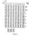
- Figure 3 shows the layout of ROM's 28-1 and 28-2 in 16-bit blocks. Each block is bit addressable by signals LWBYTE-00 and L8AD19+00 which select one of four columns and signals L8AD10+00 and L8AD09+00 which select one of four rows.
- Pattern octal 0 shows the eight solid colors made up of combinations of red, green and blue in accordance with the following table.
- a yellow pixel on display 40 is made up of a ONE bit read from bit map memory 10-R, a ONE bit read from bit map memory 10-G, and a ZERO bit read from bit map memory 10-B, the three bit map memories being addressed by the same address signals from the address MUX 6, Figure 1.
- pattern octal 0 a mosaic of pattern octal 1, that is, an area made up of 16-bit blocks, would display diagonal lines in one of eight colors.
- a mosaic of pattern octal 2 would display vertical lines in one of eight colors.
- Patterns octal 3 through octal 7 have only a percentage of the 16 bits displaying the specified color as indicated by the percentage figures on the right side of Figure 3.
- the 0 indicates a background color which may or may not be preserved, depending on the mode selected and previously described thus allowing the mixing of colors to attain many different shades and hues.
- Pattern octal 7 (25%) of white is mixed with pattern octal 3 (25%) of cyan to give a shade of pink.
- Mixing pattern octal 5 (50%) of magenta and pattern octal 4 (50%) of red gives a deep red with a blue tint.
- Also mixing pattern octal 7 (25%) of white with pattern octal 3 (25%) of cyan gives a pale cyan.
- the color is selected by signal GDAT05+00 applied to ROM 28-1 and signals GDAT06+00 and GDAT07+00 applied to ROM 28-2. Signals GDAT05+00, GDAT06+00 and GDAT07+00 determine the color octal number of Figure 3 and are received by the graphics logic from PCO interface data bus 36.
Applications Claiming Priority (2)
| Application Number | Priority Date | Filing Date | Title |
|---|---|---|---|
| US681539 | 1984-12-14 | ||
| US06/681,539 US4683466A (en) | 1984-12-14 | 1984-12-14 | Multiple color generation on a display |
Publications (2)
| Publication Number | Publication Date |
|---|---|
| EP0184857A2 true EP0184857A2 (fr) | 1986-06-18 |
| EP0184857A3 EP0184857A3 (fr) | 1988-09-28 |
Family
ID=24735698
Family Applications (1)
| Application Number | Title | Priority Date | Filing Date |
|---|---|---|---|
| EP85115932A Withdrawn EP0184857A3 (fr) | 1984-12-14 | 1985-12-13 | Génération de couleurs multiples sur un dispositif d'affichage |
Country Status (10)
| Country | Link |
|---|---|
| US (1) | US4683466A (fr) |
| EP (1) | EP0184857A3 (fr) |
| KR (1) | KR910009844B1 (fr) |
| CN (1) | CN85109708A (fr) |
| AU (1) | AU5089485A (fr) |
| CA (1) | CA1250973A (fr) |
| DK (1) | DK580885A (fr) |
| FI (1) | FI854911A (fr) |
| NO (1) | NO855029L (fr) |
| YU (1) | YU194885A (fr) |
Cited By (3)
| Publication number | Priority date | Publication date | Assignee | Title |
|---|---|---|---|---|
| EP0241655A2 (fr) * | 1986-04-11 | 1987-10-21 | International Business Machines Corporation | Fonctionnement de trame étendu dans un dispositif d'affichage |
| FR2633426A1 (fr) * | 1988-06-24 | 1989-12-29 | Japan Aviation Electron | Procede et dispositif de commande de visualisation en couleur |
| EP0435391A2 (fr) * | 1989-12-28 | 1991-07-03 | Koninklijke Philips Electronics N.V. | Dispositif d'affichage à couleurs |
Families Citing this family (19)
| Publication number | Priority date | Publication date | Assignee | Title |
|---|---|---|---|---|
| US4783652A (en) * | 1986-08-25 | 1988-11-08 | International Business Machines Corporation | Raster display controller with variable spatial resolution and pixel data depth |
| US4958302A (en) * | 1987-08-18 | 1990-09-18 | Hewlett-Packard Company | Graphics frame buffer with pixel serializing group rotator |
| EP0377038A4 (en) * | 1988-07-20 | 1991-09-18 | Ishizaka Shoji Co., Ltd. | Textile color design simulator |
| US4956638A (en) * | 1988-09-16 | 1990-09-11 | International Business Machines Corporation | Display using ordered dither |
| US5254978A (en) * | 1991-03-29 | 1993-10-19 | Xerox Corporation | Reference color selection system |
| GB2263038B (en) * | 1991-12-30 | 1996-01-31 | Apple Computer | Apparatus for manipulating streams of data |
| US5734369A (en) * | 1995-04-14 | 1998-03-31 | Nvidia Corporation | Method and apparatus for dithering images in a digital display system |
| US5784055A (en) * | 1996-05-06 | 1998-07-21 | International Business Machines Corporation | Color control for on-screen display in digital video |
| US7445551B1 (en) | 2000-05-24 | 2008-11-04 | Nintendo Co., Ltd. | Memory for video game system and emulator using the memory |
| US8133115B2 (en) | 2003-10-22 | 2012-03-13 | Sony Computer Entertainment America Llc | System and method for recording and displaying a graphical path in a video game |
| US11278793B2 (en) | 2004-03-31 | 2022-03-22 | Nintendo Co., Ltd. | Game console |
| US8267780B2 (en) | 2004-03-31 | 2012-09-18 | Nintendo Co., Ltd. | Game console and memory card |
| US20060055945A1 (en) * | 2004-09-13 | 2006-03-16 | Fazakerly William B | Color-mapped data display |
| US20060071933A1 (en) * | 2004-10-06 | 2006-04-06 | Sony Computer Entertainment Inc. | Application binary interface for multi-pass shaders |
| US7636126B2 (en) | 2005-06-22 | 2009-12-22 | Sony Computer Entertainment Inc. | Delay matching in audio/video systems |
| US7880746B2 (en) | 2006-05-04 | 2011-02-01 | Sony Computer Entertainment Inc. | Bandwidth management through lighting control of a user environment via a display device |
| US7965859B2 (en) | 2006-05-04 | 2011-06-21 | Sony Computer Entertainment Inc. | Lighting control of a user environment via a display device |
| US10786736B2 (en) | 2010-05-11 | 2020-09-29 | Sony Interactive Entertainment LLC | Placement of user information in a game space |
| US9342817B2 (en) | 2011-07-07 | 2016-05-17 | Sony Interactive Entertainment LLC | Auto-creating groups for sharing photos |
Citations (2)
| Publication number | Priority date | Publication date | Assignee | Title |
|---|---|---|---|---|
| US4183046A (en) * | 1978-08-17 | 1980-01-08 | Interpretation Systems Incorporated | Electronic apparatus for converting digital image or graphics data to color video display formats and method therefor |
| EP0095618A2 (fr) * | 1982-05-31 | 1983-12-07 | Kabushiki Kaisha Toshiba | Système de mémoire |
Family Cites Families (8)
| Publication number | Priority date | Publication date | Assignee | Title |
|---|---|---|---|---|
| US32200A (en) * | 1861-04-30 | Combined steam and hot-air engine | ||
| JPS559742B2 (fr) * | 1974-06-20 | 1980-03-12 | ||
| US4197590A (en) * | 1976-01-19 | 1980-04-08 | Nugraphics, Inc. | Method for dynamically viewing image elements stored in a random access memory array |
| USRE32200E (en) | 1980-11-03 | 1986-07-08 | Fairchild Semiconductor Corporation | MOS battery backup controller for microcomputer random access memory |
| US4429306A (en) * | 1981-09-11 | 1984-01-31 | International Business Machines Corporation | Addressing system for a multiple language character generator |
| US4516118A (en) * | 1982-08-30 | 1985-05-07 | Sperry Corporation | Pulse width modulation conversion circuit for controlling a color display monitor |
| US4521770A (en) * | 1982-08-30 | 1985-06-04 | International Business Machines Corporation | Use of inversions in the near realtime control of selected functions in interactive buffered raster displays |
| US4578673A (en) * | 1983-07-08 | 1986-03-25 | Franklin Computer Corporation | Video color generator circuit for computer |
-
1984
- 1984-12-14 US US06/681,539 patent/US4683466A/en not_active Expired - Fee Related
-
1985
- 1985-12-09 AU AU50894/85A patent/AU5089485A/en not_active Abandoned
- 1985-12-12 FI FI854911A patent/FI854911A/fi not_active IP Right Cessation
- 1985-12-13 CA CA000497571A patent/CA1250973A/fr not_active Expired
- 1985-12-13 CN CN198585109708A patent/CN85109708A/zh active Pending
- 1985-12-13 YU YU01948/85A patent/YU194885A/xx unknown
- 1985-12-13 NO NO855029A patent/NO855029L/no unknown
- 1985-12-13 KR KR1019850009367A patent/KR910009844B1/ko active IP Right Grant
- 1985-12-13 DK DK580885A patent/DK580885A/da not_active Application Discontinuation
- 1985-12-13 EP EP85115932A patent/EP0184857A3/fr not_active Withdrawn
Patent Citations (2)
| Publication number | Priority date | Publication date | Assignee | Title |
|---|---|---|---|---|
| US4183046A (en) * | 1978-08-17 | 1980-01-08 | Interpretation Systems Incorporated | Electronic apparatus for converting digital image or graphics data to color video display formats and method therefor |
| EP0095618A2 (fr) * | 1982-05-31 | 1983-12-07 | Kabushiki Kaisha Toshiba | Système de mémoire |
Cited By (5)
| Publication number | Priority date | Publication date | Assignee | Title |
|---|---|---|---|---|
| EP0241655A2 (fr) * | 1986-04-11 | 1987-10-21 | International Business Machines Corporation | Fonctionnement de trame étendu dans un dispositif d'affichage |
| EP0241655A3 (en) * | 1986-04-11 | 1990-03-21 | International Business Machines Corporation | Extended raster operating in a display system |
| FR2633426A1 (fr) * | 1988-06-24 | 1989-12-29 | Japan Aviation Electron | Procede et dispositif de commande de visualisation en couleur |
| EP0435391A2 (fr) * | 1989-12-28 | 1991-07-03 | Koninklijke Philips Electronics N.V. | Dispositif d'affichage à couleurs |
| EP0435391A3 (en) * | 1989-12-28 | 1991-10-23 | N.V. Philips' Gloeilampenfabrieken | Color display apparatus |
Also Published As
| Publication number | Publication date |
|---|---|
| FI854911A0 (fi) | 1985-12-12 |
| US4683466A (en) | 1987-07-28 |
| CN85109708A (zh) | 1986-12-17 |
| DK580885A (da) | 1986-06-15 |
| AU5089485A (en) | 1986-06-19 |
| EP0184857A3 (fr) | 1988-09-28 |
| KR910009844B1 (ko) | 1991-11-30 |
| DK580885D0 (da) | 1985-12-13 |
| FI854911A (fi) | 1986-06-15 |
| CA1250973A (fr) | 1989-03-07 |
| YU194885A (en) | 1988-10-31 |
| NO855029L (no) | 1986-06-16 |
| KR860005281A (ko) | 1986-07-21 |
Similar Documents
| Publication | Publication Date | Title |
|---|---|---|
| US4683466A (en) | Multiple color generation on a display | |
| US4217577A (en) | Character graphics color display system | |
| US5132674A (en) | Method and apparatus for drawing high quality lines on color matrix displays | |
| US4554538A (en) | Multi-level raster scan display system | |
| US4542376A (en) | System for electronically displaying portions of several different images on a CRT screen through respective prioritized viewports | |
| US4550315A (en) | System for electronically displaying multiple images on a CRT screen such that some images are more prominent than others | |
| US4559533A (en) | Method of electronically moving portions of several different images on a CRT screen | |
| US4933878A (en) | Graphics data processing apparatus having non-linear saturating operations on multibit color data | |
| US4718024A (en) | Graphics data processing apparatus for graphic image operations upon data of independently selectable pitch | |
| EP0258560B1 (fr) | Contrôleur d'affichage à trames avec résolution spatiale variable et avec profondeur des données des éléments d'image variable | |
| KR900000742B1 (ko) | 그래픽스(graphics)의 표시장치 | |
| US4763283A (en) | Color transcoding process permitting the interconnection of two definition equipments of different colors and the corresponding transcoder | |
| US4757470A (en) | Pattern generation for a graphics display | |
| US4757309A (en) | Graphics display terminal and method of storing alphanumeric data therein | |
| US5185859A (en) | Graphics processor, a graphics computer system, and a process of masking selected bits | |
| EP0182375B1 (fr) | Dispositif de mémorisation de données multi-bit d'éléments d'image | |
| EP0093954A2 (fr) | Mémoire d'affichage d'image | |
| EP0256838B1 (fr) | Système pour améliorer le fonctionnement des affichages à deux couleurs | |
| CA1233279A (fr) | Appareil a ecran de visualisation polychrome | |
| EP0360530A2 (fr) | Dispositif de commande d'affichage programmable à formats multiples | |
| US4788536A (en) | Method of displaying color picture image and apparatus therefor | |
| US4291306A (en) | Figure displaying device | |
| EP0170977A2 (fr) | Sous-système d'affichage | |
| EP0189567B1 (fr) | Système d'affichage en couleur | |
| JPH0352067B2 (fr) |
Legal Events
| Date | Code | Title | Description |
|---|---|---|---|
| PUAI | Public reference made under article 153(3) epc to a published international application that has entered the european phase |
Free format text: ORIGINAL CODE: 0009012 |
|
| AK | Designated contracting states |
Kind code of ref document: A2 Designated state(s): CH DE FR GB IT LI NL SE |
|
| RAP1 | Party data changed (applicant data changed or rights of an application transferred) |
Owner name: HONEYWELL BULL INC. |
|
| PUAL | Search report despatched |
Free format text: ORIGINAL CODE: 0009013 |
|
| AK | Designated contracting states |
Kind code of ref document: A3 Designated state(s): CH DE FR GB IT LI NL SE |
|
| 17P | Request for examination filed |
Effective date: 19890328 |
|
| STAA | Information on the status of an ep patent application or granted ep patent |
Free format text: STATUS: THE APPLICATION IS DEEMED TO BE WITHDRAWN |
|
| 18D | Application deemed to be withdrawn |
Effective date: 19900703 |
|
| RIN1 | Information on inventor provided before grant (corrected) |
Inventor name: HOLTEY, THOMAS O. Inventor name: BRUCE, KENNETH E. Inventor name: GOSS, GARY J. |