EP0184828B1 - Vector processing apparatus - Google Patents
Vector processing apparatus Download PDFInfo
- Publication number
- EP0184828B1 EP0184828B1 EP85115752A EP85115752A EP0184828B1 EP 0184828 B1 EP0184828 B1 EP 0184828B1 EP 85115752 A EP85115752 A EP 85115752A EP 85115752 A EP85115752 A EP 85115752A EP 0184828 B1 EP0184828 B1 EP 0184828B1
- Authority
- EP
- European Patent Office
- Prior art keywords
- elements
- vector
- address
- instruction
- data
- Prior art date
- Legal status (The legal status is an assumption and is not a legal conclusion. Google has not performed a legal analysis and makes no representation as to the accuracy of the status listed.)
- Expired - Lifetime
Links
- 239000013598 vector Substances 0.000 title claims description 130
- 238000012545 processing Methods 0.000 title claims description 59
- 239000000872 buffer Substances 0.000 claims description 57
- 230000015654 memory Effects 0.000 claims description 11
- 238000013519 translation Methods 0.000 claims description 11
- 238000003860 storage Methods 0.000 description 69
- 101000685663 Homo sapiens Sodium/nucleoside cotransporter 1 Proteins 0.000 description 12
- 101000822028 Homo sapiens Solute carrier family 28 member 3 Proteins 0.000 description 12
- 102100023116 Sodium/nucleoside cotransporter 1 Human genes 0.000 description 12
- 102100021470 Solute carrier family 28 member 3 Human genes 0.000 description 12
- 238000010586 diagram Methods 0.000 description 10
- FFKXTXJQZGIKQZ-UHFFFAOYSA-N ROPA Natural products O1C2C3C=C(CO)CC(C(C(C)=C4)=O)(O)C4C3(O3)C(C)CC2(C(C)=C)OC31CC1=CC=CC=C1 FFKXTXJQZGIKQZ-UHFFFAOYSA-N 0.000 description 9
- 101000821827 Homo sapiens Sodium/nucleoside cotransporter 2 Proteins 0.000 description 6
- 102100021541 Sodium/nucleoside cotransporter 2 Human genes 0.000 description 6
- 230000009977 dual effect Effects 0.000 description 6
- 101100382854 Arabidopsis thaliana CCD7 gene Proteins 0.000 description 5
- 101100129499 Arabidopsis thaliana MAX2 gene Proteins 0.000 description 5
- 238000000034 method Methods 0.000 description 5
- 101100129496 Arabidopsis thaliana CYP711A1 gene Proteins 0.000 description 4
- 101100083446 Danio rerio plekhh1 gene Proteins 0.000 description 4
- 230000014759 maintenance of location Effects 0.000 description 4
- 238000007781 pre-processing Methods 0.000 description 3
- 230000006870 function Effects 0.000 description 2
- 238000012805 post-processing Methods 0.000 description 2
- 101001047084 Mus musculus Potassium voltage-gated channel subfamily H member 2 Proteins 0.000 description 1
- 238000010276 construction Methods 0.000 description 1
- 230000003111 delayed effect Effects 0.000 description 1
- 238000001514 detection method Methods 0.000 description 1
- 238000011161 development Methods 0.000 description 1
- 230000018109 developmental process Effects 0.000 description 1
- 239000000284 extract Substances 0.000 description 1
- 238000012544 monitoring process Methods 0.000 description 1
- 238000012546 transfer Methods 0.000 description 1
Images


Classifications
-
- G—PHYSICS
- G06—COMPUTING; CALCULATING OR COUNTING
- G06F—ELECTRIC DIGITAL DATA PROCESSING
- G06F9/00—Arrangements for program control, e.g. control units
- G06F9/06—Arrangements for program control, e.g. control units using stored programs, i.e. using an internal store of processing equipment to receive or retain programs
- G06F9/30—Arrangements for executing machine instructions, e.g. instruction decode
- G06F9/30003—Arrangements for executing specific machine instructions
- G06F9/30007—Arrangements for executing specific machine instructions to perform operations on data operands
- G06F9/30021—Compare instructions, e.g. Greater-Than, Equal-To, MINMAX
-
- G—PHYSICS
- G06—COMPUTING; CALCULATING OR COUNTING
- G06F—ELECTRIC DIGITAL DATA PROCESSING
- G06F15/00—Digital computers in general; Data processing equipment in general
- G06F15/76—Architectures of general purpose stored program computers
- G06F15/80—Architectures of general purpose stored program computers comprising an array of processing units with common control, e.g. single instruction multiple data processors
- G06F15/8053—Vector processors
- G06F15/8076—Details on data register access
-
- G—PHYSICS
- G06—COMPUTING; CALCULATING OR COUNTING
- G06F—ELECTRIC DIGITAL DATA PROCESSING
- G06F9/00—Arrangements for program control, e.g. control units
- G06F9/06—Arrangements for program control, e.g. control units using stored programs, i.e. using an internal store of processing equipment to receive or retain programs
- G06F9/30—Arrangements for executing machine instructions, e.g. instruction decode
- G06F9/30003—Arrangements for executing specific machine instructions
- G06F9/30007—Arrangements for executing specific machine instructions to perform operations on data operands
- G06F9/30032—Movement instructions, e.g. MOVE, SHIFT, ROTATE, SHUFFLE
-
- G—PHYSICS
- G06—COMPUTING; CALCULATING OR COUNTING
- G06F—ELECTRIC DIGITAL DATA PROCESSING
- G06F9/00—Arrangements for program control, e.g. control units
- G06F9/06—Arrangements for program control, e.g. control units using stored programs, i.e. using an internal store of processing equipment to receive or retain programs
- G06F9/30—Arrangements for executing machine instructions, e.g. instruction decode
- G06F9/30003—Arrangements for executing specific machine instructions
- G06F9/30007—Arrangements for executing specific machine instructions to perform operations on data operands
- G06F9/30036—Instructions to perform operations on packed data, e.g. vector, tile or matrix operations
Definitions
- the present invention relates to a vector processing apparatus.
- a vector processing apparatus which is a combination of a general purpose scalar data processing unit and an operation unit for processing vector elements has been known (Japanese Patent Kokoku Nos. 58-52265 and 59-25264).
- indices of vector operands are uniformly incremented to process the vector elements.
- a high speed vector operation is not attained.
- a further vector processor is disclosed in EP 0149213 which falls under Article 54(3) EPC.
- the vector processor comprises memory means for storing vector operands, operating means for for storing vector operands, operating means for performing compare and select operations on the basis of first and second vector operands from the memory means and outputting a third vector operand obtained as the result of the operations to the memory means, first to third indication means for indicating element numbers of the first to third vector operands which are being processed at present by the operating means and control means for respectively independently controlling the respective ones of the first to third indication means.
- computer systems include a storage hierarchy, processing units, I/O controls and a CPU (central processing unit) for executing instructions.
- This system includes a VMR (vector mask register) storage connected to the CPU for storing a set of results representative of the results of the execution of the instruction and a counting and address storing apparatus connected to the VMR storage for monitoring the storage of the set of results, the counting and address storing apparatus generates and stores information related to the set of results simultaneously with the storage of the set of results in the VMR storage, whereby the information is immediately available upon the completion of the storage of the set of results.
- VMR vector mask register
- the object of the present invention is to provide a vector processing apparatus which enables vector operation of a type in which increment of vector indices depends on an operation result of data.
- vector operands designated by an instruction are sequentially fetched from a memory to vector processing means and held in a buffer in the vector processing means.
- the vector processing means reads out elements of the vector operands from the buffer and operates them, for example, compares two elements. In accordance with an operation result, the vector processing means controls fetching of the vector elements to be processed next, from the buffer.
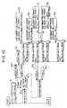
- Fig. 1 shows an overall configuration of one embodiment of the present invention.
- Numeral 9 denotes a main storage
- numeral 8 denotes a storage control unit
- numeral 10 denotes an input/output processor
- numeral 11 denotes a scalar processor
- numeral 7 denotes a vector processor for exclusively processing vector data.
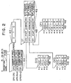
- Fig. 2 shows a MERGE SORT instruction format and the operation thereof.
- the MERGE SORT instruction is of four-byte (4B) length.
- the 0-15th bits of the instruction include an operation code which specifies the MERGE SORT instruction.
- the 16th-23rd bits of the instruction have no meaning.
- the numbers of processed operands of vector operands are contained in three general purpose registers having serial numbers starting from the number specified by the 24-27th bits (R1 field) of the instruction.
- a description table origin (DTO) of a description table (DT) is contained in a general purpose register having the number specified by the 28th-31th bits (R2 field) of the instruction.
- the general purpose registers are provided in a general purpose register unit 4.
- the DT specified by the DTO is on the main storage 9 and contains start addresses of the vector operands and maximum number of elements.
- the vector operand indirectly specified by the DT includes a first four-byte integer field without a sign for identifying a data and a second four-byte numeric data field to be sorted.
- Maximum number of elements for OP2 4
- Maximum number of elements for OP3 4
- Maximum number of elements for OP1 8 where OP2, OP3 and OP1 represent second, third and first operands, respectively.
- the OP2 element and the OP3 element are compared and a smaller one is stored. (If both are equal, the OP2 element is stored.)
- the #0 data field of the OP2 and the #0 data field of the OP3 are compared and the data of the OP2 is selected and stored.
- the next comparison is made between the next element of the selected operand and the previous element of the non-selected operand.
- the #1 of the OP2 and the #0 of the OP3 are compared. This operation is continued until all elements of the OP2 and OP3 are stored.
- the MERGE SORT instruction can be considered as an instruction to produce a longer sorted vector from two shorter sorted vectors.
- the MERGE SORT instruction is effective in table sorting in a relational data base.
- the MERGE SORT instruction is a vector instruction of a type in which the increment of the numbers of processed elements of the OP2 and OP3 depends on the comparison result of the OP2 and OP3.
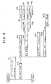
- Fig. 3 shows an operation of the MERGE SORT instruction by a Program Analysis Diagram (PAD). Symbols used in Fig. 3 correspond to those of Fig. 2 as follows.
- PAD Program Analysis Diagram
- the end of the processing in P12 may be arbitrarily defined. For example, it may be terminated on the condition of "k ⁇ k max ".
- the increments of i and j are not uniform and depend on the comparison result of A(i) and B(j).
- the instruction fetched from the buffer storage control unit 1 through a path 13 is decoded by an instruction unit 3. If it is decoded as the MERGE SORT instruction, the instruction unit 3 informs to the execution unit 5 of the MERGE SORT instruction and register numbers (R1 and R2 fields) to be used, through a path 35 and passes the control to the scalar execution unit 5.
- the instruction unit 3 informs to the execution unit 5 of the MERGE SORT instruction and register numbers (R1 and R2 fields) to be used, through a path 35 and passes the control to the scalar execution unit 5.
- the scalar execution unit 5 sends the register numbers in the R1 and R2 fields informed by the instruction unit 3 to the GPR 4 through a path 54E to read out the content of the GPR 4 through a path 45.
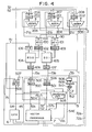
- Fig. 4 shows a detailed configuration of the address control unit 2, buffer storage control unit 1 and execution unit 5 of Fig. 1.
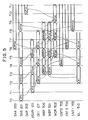
- Fig. 5 is a time chart for illustrating the operation of Fig. 4. The operation of Fig. 1 is explained in detail with reference to Figs. 4 and 5.
- OP2A represents a start address of the OP2.
- OP3A represents a start address of the OP3.
- OP1A represents a start address of the OP1.
- GR(R1) represents the number of processed elements of the OP2.
- GR(R1+1) represents the number of processed elements of the OP3.
- GR(R1+2) represents the number of processed elements of the OP1.
- OP2A' represents a start address of the unprocessed elements of the OP2.
- OP3A' represents a start address of the unprocessed elements of the OP3.
- OP1A' represents a start address of the unprocessed elements of the OP1.
- the register numbers in the R1 and R2 fields transferred from the instruction unit 3 through the path 35 are set in a register 508.
- the operation code is sent to the vector processor 7.
- a selector 509 first selects the R2 field and sets the content of the R2 field to an EL register 510.
- the content of the EL 510 is sent to the GPR 4 through the path 54E, reads out the DTO through the path 45 and sets it to a work register B (WBR) 501 through a selector 506.
- the DTO set in the WBR 501 is selected by a selector 504 and it is set in a fetch-only address register B(SAB) 201 (Fig. 5) in the address control unit 2 through a selector 207.
- SAA 200 Another fetch-only address register (SAA) 200 is provided in the address control unit 2 so that those registers correspond to two address translation units and two buffer storages in the buffer storage control unit 1. Those two address translation units and two buffer storages are functionally identical, respectively, and they are duplicated to attain a high speed processing of the elements.
- the dual units are referred to as 0-system and 1-system.
- the DTO fetch uses the 1-system.
- the content (DTO) of the SAB 201 is sent to the buffer storage control unit 1 through a path 21b.
- the DTO is translated by the address translation unit AT1 101 from a virtual address to a real address, which is set in a buffer storage address register BSAR1 103. (Fig. 5 T1).
- the buffer storage BS1 105 is accessed by the content (DTO) of the BSAR1 103 and the data read therefrom is set in the 8-byte readout data register DR1 107 (Fig. 5 T2).
- the start address of the OP2 is set in the first four bytes of the DR1 107 and the maximum number of elements of the OP2 is set in the second four bytes.
- the data read from the DR 1.107 is sent to the scalar execution unit 5 through the path 156.
- the buffer storages BSO 104 and BSI 105 contain partial copies of the main storage. If the data to be accessed is not in the buffer storages, the data is transferred from the main storage unit 9 under the control of the buffer storage control unit 1.
- the scalar execution unit 5 sets the data sent through the path 15b in the WBR 501 (Fig. 5 T3).
- the scalar execution unit 5 selects the R1 field held in the register 508 by the selector 509 and sets it in the EL register 510. (Fig. 5 T2).
- the content (the number of processed elements of the OP2) of the general purpose register designated by the R1 field is read out by the EL register 510 through the path 45 and it is set in the work register A (WAR) 500 through the selector 505 (Fig. 5 T3).
- the content of the WAR 500 is multiplied by the number of elements (8) by an operation unit 503 and the result is set in the WAR 500 through the selector 505 (Fig. 5 T4).
- the content of the WAR 500 and the first four bytes (start address of the OP2) are added by the operation unit 503 and the sum is set in the work register C (WCR) 502 through the selector 507. (Fig. 5 T5).
- the number of processed elements read from the GPR 4 into the WAR 500 is normally zero and the product after the multiplication by the number of elements is also zero.
- the MERGE SORT instruction is interrupted, the number of elements processed so far is held in the GPR 4. Accordingly, when the process is resumed, the number of processed elements multiplied by the number of elements is added to the start address specified by the DT to create the address of the resumed element.
- the content of the WCR 502 is selected by the selector 504 and transferred to the SAA 200 in the address control unit 2 through the path 52 and the selector 206. (Fig. 5 T6).
- the second four bytes (maximum number of elements of the OP2) of the WBR 501 are selected by the selector 504 and transferred to the vector processor 7 through the path 57.
- the next eight bytes of the DT are read out in overlap with the readout of the first eight bytes. This is shown in Fig. 5.
- the +8 and +16 operations of the DTO are carried out by the operation unit 204 in the address control unit 2.
- the vector operand address at which the processing is to start is set in the SAA 200, SAB 201 and the store only address register (DAR) 202 in the address register control unit 2.
- the contents of the three general purpose registers having serial numbers starting from the number specified by the R1 field of the instruction are serially read from the GPR 4 into the scalar processing unit 5 through the path 45 and sent to the vector processor 7 through the selector 504 and the path 57.
- the +1 and +2 operations of the R1 field are carried out by the operation unit 512.
- Fig. 6 shows an internal configuration of the vector processor 7.
- the maximum numbers of elements of the operands sent from the scalar execution unit 5 through the path 57 are set in maximum number of elements registers MAX2 700, MAX3 701 and MAX1 702, and the numbers of processed elements of the operands are set in element counters CNT2 703, CNT3 704 and CNT1 705.
- a fetch request addressed by the SAA 200 and SAB 201 is issued to the buffer storage control unit 1 from the address control unit 2 under the control of the scalar execution unit 5.
- the SAA 200 and SAB 201 contain the start addresses of the unprocessed elements of the OP2 and OP3, respectively.
- the buffer storage control unit 1 translate the content of the SAA 200 sent through the path 21a by the address translation unit (ATO) 100 and sets the translated address in the BSARO 102, and it accesses the BSO 104 by the translated address and sets the read data in the DRO 106. It also accesses the BS1 105 by the content of the SAB 201 sent through the path 21b and sets the read data in the DR1 107.
- the DRO 106 and DR1 107 contain the start elements of the unprocessed elements of the OP2 and OP3, respectively.
- the scalar execution unit 5 reads out the content of the DRO 106 through the path 15a and sets it in the WAR 500. It also reads out the content of the DR1 107 through the path 15b and sets it in the WBR 501.
- the scalar execution unit 5 sends the data to the vector processor 7 through the paths 57a and 57b.
- the vector processor 7 receives the vector operand data through the paths 57a and 57b, it compares the second four bytes of the data and sends a smaller data (OP2 elements if both are equal) to the scalar execution unit 5 through the path 75.
- the address control unit 2 sends a store request addressed by the DAR 202 to the buffer storage control unit 1 under the control of the scalar execution unit 5.
- the DAR 202 points the start address of the unprocessed elements of the OP3.
- the data stored in the WCR 502 is set in the write data register (FR) 108 in the buffer storage control unit 1 under the instruction of the scalar execution unit 5.
- the buffer storage control unit 1 translates the address sent from the address control unit 2, and if the translated address is in the BSO 104 and BS1 105, it writes the content of the FR 108. It also sends the store request to the main storage 9.
- the registers and paths other than those of the vector processor 7 utilize resources which are usually used in executing the scalar instructions.
- the data are transferred under the control of the scalar execution unit 5.
- the OP2 element and the OP3 element are compared and a smaller one (the OP2 element if both are equal) is selected and stored.
- the OP2 #0 element and the OP3 #0 element are compared, and the smaller one, the OP2 element, is selected and stored.
- the next element of the selected operand and the precious element of the non-selected operand are compared.
- the OP2 #1 element and the OP3 #0 element are compared.
- control lines 72a and 72b which indicate which one of the OP2 and OP3 was selected in the comparison in the vector processor 7 to the address control unit 2 are provided so that the comparison result in the vector processor 7 is reflected to the updating of the address register in the address control unit 2.
- the OP2 #0 element and the OP3 #0 element are compared, the OP2 element is selected, the SAA 200 which holds the OP2 address is incremented by 8 through the control line 72a, and the fetch request for the OP2 #1 element is sent out. In this method, however, a high speed pipeline operation is not attained.
- the operand address register for the selected operand is not updated but the updating of the operand register for the non-selected operand is suppressed and the fetch request is sent out in each cycle. Namely;
- the vector processor 7 needs a buffer to store necessary data.
- the updating of the address register is suppressed and the fetch request is issued each cycle, the same data is read out repeatedly.
- the vector processor 7 By controlling the vector processor 7 such that it does not fetch the data from the scalar execution unit 5, the fetching of unnecessary data into the operand buffer is prevented.
- Fig. 6 shows an embodiment of the vector processor 7.
- Numeral 707 denotes an operand buffer A (ROBA) for storing the OP2 data
- numeral 708 denotes an operand buffer B (ROBB) for storing the OP3 data.
- the ROBA 707 and ROBB 708 can hold five elements #0 - #4, respectively. They receive and hold the OP2 data and the OP3 data sent from the scalar execution unit 5 through the paths 57a and 57b, respectively.
- An in-pointer 719 is a 3-bit counter which is wrapped around from 4 to 0. The data sent from the path 57a is set at a data position in the ROBA 707 designated by the in-pointer 719.
- An in-pointer 720 is a counter which is identical in construction to the in-pointer 719.
- the data from the path 57b is set at a data position of the ROBB 708 designated by the in-pointer 720.
- the in-pointers 719 and 720 are incremented by one, respectively.
- the setting of the data into the ROBA 707 and the ROBB 708 is effected by outputs of delay circuits 726 and 727.
- An out-pointer (ROPA) 706 and an out-pointer (ROPB) 709 are 3-bit counters which wrap around from 4 to 0.
- the outputs of the ROPA 706 and ROPB 709 are supplied to selectors 710 and 711, respectively, which read out the elements at data positions of the ROBA 707 and ROBB 708 designated by the ROPA 706 and ROPB 709, respectively.
- the ROBA 707 and ROBB 708 are of FIFO (first-in first-out) type.
- the element data from the selectors 710 and 711 are compared by a comparator 712.
- the comparison result of the comparator 712 is supplied to a decision circuit 713.
- the decision circuit 713 activates a selector 714 through a path 725 in accordance with the comparison result of the comparator 712 so that a smaller element data is set in a register 715.
- a time chart shown in Fig. 7 The operation of the vector processor 7 shown in Fig. 6 is explained with reference to a time chart shown in Fig. 7.
- the OP2 and OP3 are those shown in Fig. 2 and the numbers of unprocessed elements of the OP2 and OP3 are zero, respectively.
- the data arrives at the vector processor 7 in the cycle 4.
- the OP2 element #0 and the OP3 element #0 are read into the DR0 and DR1, respectively in the cycle 2 at the OP2 address OP2A' and the OP3 address OP3A' designated by the SAA 200 and the SAB 201, respectively, in the cycle 0.
- they are transferred to the WAR and WBR, and in the cycle 4, they are set in the ROBA and ROBB, respectively.
- they are read from the ROBA and ROBB and compared. If the OP2 element is selected as a result of the comparison of the OP2 and OP3 elements by the comparator 712, the decision circuit 713 operates as follows.
- the operand data fetched by the fetch request for the element #1 - #4 of the OP3 are sequentially set in the ROBB 708 until the output 72b is reflected to the updating of the address register.
- the fetch request for the element #5 of the OP3 is also issued and the operand data fetched thereby is set in the WBR 501 of the scalar processing unit 5 but it is not set in the ROBB 708, because the output 72b of the decision circuit 713 is supplied to the ROBB 708 through the delay 727 four cycles later to suppress the setting into the ROBB 708.
- the ROBB 708 requires a memory capacity of at least (the number of fetch requests overrun -1) x 8 bytes, that is, 40 bytes.
- the ROBA 707 operates in a similar manner and is controlled by a 4-cycle delay 726.
- the ROPA 706 is incremented by one and the ROPB 709 is not updated.
- the element #1 of the OP2 and the element #0 of the OP3 are next compared.
- the following operation takes place.
- the operation continues as shown in Fig. 7.
- the ROPA 706 and ROPB 709 which instruct the elements to be next processed after fetched from the buffers 707 and 708 are not uniformly incrmented each cycle but are controlled in accordance with the comparison result of the comparator 712. Similarly, the updating of the element counters 703 and 704 is controlled.
- the MERG SORT instruction can be processed at one machine cycle pitch.
- Fig. 6 the detection of the end of operation is explained.
- the outputs of the comparators 716, 717 and 718 are supplied to the decision circuit 713.
- the element counters CNT2 703, CNT3 704 and CNT1 705 are counted up as shown in Fig. 7. If the comparison of the CNT2 703 of the OP2 and the MAX2 700 of the OP2 by the comparator 716 shows equal and the comparison of the CNT3 704 of the OP3 and the MAX3 701 of the OP3 by the comparator 717 shows equal, the absence of effective element is informed to the scalar execution unit 5 through the line 72c in synchronism with the sending of the store request from the WCR 502 of the last element.
- the scalar execution unit 5 stops to send the data stored in the WCR 502 and starts the end processing.
- the contents of the counters CNT2 703, CNT3 704 and CNT1 705 for the respective operands in the vector processor 7 are sequentially read out through the selector 714 under the control of the scalar execution unit 5, set in the WCR 502 through the path 75, sent to the GPR 4 through the path 54 and written into three general purpose registers having serial numbers starting from the number specified by the R1 field of the instruction. After all counts have been written into the three general purpose registers, the execution unit 5 informs the end of the MERGE SORT instruction to the instruction unit 5.
- Fig. 8 shows another embodiment of the present invention.
- the configuration of Fig. 8 is similar to that of Fig. 1.
- Numeral 1011 denotes a scalar processor which comprises a buffer storage control unit 1001, an address control unit 1002, an instruction unit 1003, general purpose registers (GPR) 1004 and an execution control unit 1005.
- the scalar processor 1011 reads and writes data from and to a main storage 1009 through a storage control unit 1008 together with an input/output processor 1010.
- a vector processor 1007 is connected to the execution control unit 1005 of the scalar processor 1011.
- the vector processor 1007 performs a new type of vector operation in which an element number to be processed is determined by an operation result of the previous vector elements.
- Fig. 9 shows a format of the MERGIN JOIN instruction and the operation thereof.
- the MERGE JOIN instruction is of 4-byte length and the format thereof is identical to that of the MERGE SORT instruction.
- the bits 16 - 23 of the instruction have no meaning.
- the general purpose registers having four serial numbers starting from the number specified by the bits 24 - 27 (R1 field) of the instruction designates a primary element counter of a second operand (OP2 first counter), an element counter of a third operand (OP3 counter), an element counter of a first operand (OP1 counter) and a secondary element counter of the second operand (OP2 second counter). Two counters are required for the second operand to enable back tracking.
- the general purpose register specified by the bit 28 - 31 designates a description table origin (DTO) which is a start address of a description table (DT).
- the DT is on the main storage 1009 and contains the start address of the vector operand and the maximum number of elements.
- the vector operand indirectly specified by the DT is a dual vector data in which first four-byte contain an integer without sign to identify the data and second four bytes contain the data to be compared. In a simple example, the first four bytes contain a name code and the second four bytes contain his or her payroll. In another example, the first four bytes contain a mechanical part code and the second four bytes contains a price thereof. In Fig.
- "#" represents the element number.
- the first four bytes of the vector data are called a front part and the second four bytes are called a rear part.
- the vector having the two parts, front part and rear part, is called a dual vector.
- the MERGE JOIN instruction compares the rear parts of the two dual vectors for the OP2 and OP3 having the rear parts thereof sorted, and if they are equal, extracts the front parts of the respective dual vectors to produce a new dual vector (OP1).
- the MERGE JOIN instruction is effective in the table join processing in the relational data base.
- Fig. 10 is a program analysis diagram which illustrates the operation of the MERGE JOIN instruction.
- n1, n2, n3 and n4 represent initial values of the element counters which hold the element numbers, and they are integers.
- the MERGE JOIN instruction is also a vector instruction of a type in which the increment of i and j depends on the comparison result of the rear parts of A(i) and B(j).
- the instruction fetched from the buffer storage control unit 1001 through the path 1013 is decoded by the instruction unit 1003. If it is decoded as the MERGE JOIN instruction, the instruction unit 1003 informs to the execution unit 1005 through the path 1035 that it is the MERGE JOIN instruction and sends the register numbers (R1 and R2 fields) to be used to the execution unit 1005, which sends the register numbers of the R1 and R2 fields sent from the instruction unit 1003 to the GPR 1004 through the path 1054 to read out the content of the GPR 1004 through the path 1045.
- the instruction unit 1003 informs to the execution unit 1005 through the path 1035 that it is the MERGE JOIN instruction and sends the register numbers (R1 and R2 fields) to be used to the execution unit 1005, which sends the register numbers of the R1 and R2 fields sent from the instruction unit 1003 to the GPR 1004 through the path 1054 to read out the content of the GPR 1004 through the path 1045.
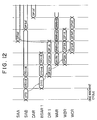
- Fig. 11 shows a detail of the buffer storage control unit 1001, address control unit 1002 and execution unit 1005 of Fig. 8.
- the path 1035 is connected to a control circuit 1036 which comprises the registers 508 and 510, selector 509 and operation unit 512 shown in Fig. 4.
- the control circuit 1036 sends the register number in the R2 field to the GPR 1004 through the path 1054E.
- the DTO sent from the GPR 1004 through the path 1045 is set in a work register (WBR) 1501 in the execution unit 1005.
- the content (OP2 first counter) of the GPR 1004 specified by the R1 field of the MERGE JOIN instruction is set in a work register (WAR) 1500.
- the DTO set in the WAR 1501 is set in a fetch-only address register (SAB) 1201 in the address control unit 1002 through the path 1052.
- the content DTO of the SAB 1201 is sent to the buffer storage control unit 1001 through a path 1021b.
- the DTO is translated by an address translation unit (AT1) 1101 from a virtual address to a real address, and the translated real address is set in a buffer address register (BSAR 1) 1103.
- a buffer storage (BS1) 1105 is accessed by the content (DTO) of the BSAR1 1103 and the read data is set in an 8-byte data register (DR1) 1107.
- first four bytes of the DR1 1107 contain the OP2 start address and second four bytes contains the maximum number of elements of the OP2.
- the data of the DR1 1107 is sent to the execution unit 1005 through the path 1015b.
- the buffer storage control unit 1001 includes address translation unit AT0 1100, buffer storage address register BSARO 1102, buffer storage BSO 1104 and data register DRO 1106 which are functionally identical to the AT1 1101, BSAR1 1103, BS1 1105 and DR1 1107, as the previous embodiment does.
- the BSO 1104 and BS1 1105 are high speed memories for storing partial copies of the main storage 1009. If the data to be accessed is not contained in the BSO or BS1, it is transferred from the main storage 1009 under the control of the buffer storage control unit 1001.
- the execution unit 1005 sets the data sent through the path 1015b in the WBR 1501, add the content of the general purpose register sepcified by the R1 field set in the WAR 1500, multiplied by the length of the element (that is, 8) to the first four bytes (OP2 start address) of the WBR 1501 by an adder 1503, and set a sum in a work address register (WCR) 1502.
- the content of the WCR 1502 is selected by a selector 1504 and transferred to a fetch-only address register (SAA) 1200 in the address control unit 1002 through a path 1052.
- SAA fetch-only address register
- the second four bytes (maximum number of elements of the OP2) of the WBR 1501 is transferred the vector processor 1007 through a path 1057.
- OP2A represents the OP2 start address
- OP3A represents the OP3 start address
- OP1A represents the OP1 start address
- GR(R1) represents the OP2 first counter content
- GR(R1+1) represents the OP3 counter content
- GR(R1+2) represents the OP1 counter content
- GR(R1+3) represents the OP2 second counter content
- OP2A' represents the start address of the OP2 unprocessed elements
- OP3A' represents the start address of the OP3 unprocessed elements
- OP1A' represents the start address of the OP1 unprocessed elements
- the vector operands to start the first processing are set in the SAA 1200, SAB 1201 and DAR 1202 in the address register control unit 1002.
- the contents of four general purpose registers having serial numbers starting from the number specified by the R1 field of the instruction are sequentially read into the execution unit 1005 through the path 1045 and sent to the processor 1007 through the selector 1504 and the path 1057.
- Fig. 13 shows an internal configuration of the vector processor 1007.
- the maximum numbers of elements of the operands sent from the execution unit 1005 through the path 1057 are set in maximum number of element registers MAX2 1700, MAX3 1701 and MAX1 1702, and the counts of the operands are set in the element counters CNT2P 1703, CNT3 1704, CNT1 1705 and CNT2S 1706 which determine the end, and in CNT2S1 1727, CNT3S 1728, CNT1S 1729 and CNT2S2 1730 which count the numbers of processed elements.
- a fetch request addressed by the SAA 1200 and SAB 1201 is issued to the buffer storage control unit 1001 from the address control unit 1002.
- the SAA 1200 and SAB 1201 contain the start address of the OP2 unprocessed elements and the start address of the OP3 unprocessed elements.
- the buffer storage control unit 1001 translates the content of the SAA 1200 sent through the path 1021a by the ATO 1100, sets the translated address in the BSAR 1102, accesses the BSO 1104 by that address and sets the read data in the DRO 1106. It also accesses the BS1 1105 by the content of the SAB 1201 sent through the path 1021b and sets the read data in the DR1 1107.
- DRO 1106 contains the start element of the OP2 unprocessed elements and the DR1 1107 contains the start element of the OP3 unprocessed elements.
- the compare operation in the vector processor 1007 is not delayed and the data can be supplied without delay.
- the execution unit 1005 reads out the content of the DRO 1106 through the path 1015a and sets it in the WAR 1500. It also reads out the content of the DR1 1107 through the path 1015b and sets it in the WBR 1501. Then, the execution unit 1005 instructs to the vector processor 1007 to fetch the data through the paths 1057a and 1057b.
- the vector processor 1007 When the vector processor 1007 receives the vector operand data sent through the paths 1057a and 1057b, it starts to compare the rear parts (second four bytes) of the operands, and if the rear parts of the OP2 and OP3 are equal, it combines front parts of the operands into an 8-byte data and sends to the execution unit 1005 a compare result signal through the path 1075a and the stored data through the path 1075.
- the execution unit 1005 When the execution unit 1005 receives the compare result siganl indicating that the rear parts of the OP2 and OP3 are equal through the path 1075a, it sends a store request to the store request control circuit 1109 of the buffer storage control unit 1001 through the store request control circuit 1505 and the path 1051. It also sets the stored data sent from the vector processor 1007 through the path 1075 in the FR 1108 of the buffer storage control unit 1001 through the WCR 1502 and the path 1051a. It further sends the store address in the store address register (DAR) 1202 of the address control unit 1002 to the buffer storage control unit 1001. The DAR 1202 now points the start address of the OP1 unprocessed elements.
- DAR store address register
- the buffer storage control unit 1001 translates the address sent from the address control unit 1002, and if the translated address is in the BSO 1104 or BS1 1105, it writes the content of the FR 1108 into the corresponding BS. It also sends the store request to the main storage control unit 1008 through the path 1001a and sends the store data through the path 1001c to write it into the main storage 1009. After the storage of the data into the main storage 1009, an end of store signal is sent from the main storage control unit 1008 to the buffer storage control unit 1001 through the path 1001b.
- the store request control circuit 1505 of the execution unit 1005 responds to the compare result signal sent from the vector processor 1007 through the path 1075a to add an "invalid" additional information to the store request and sends it to the buffer storage control unit 1001 through the path 1051.
- the vector processor 1007 sends a suppress signal for the updating of the store address to the address control unit 1002 through the path 1072a.
- a desired data is not always present in the main storage but it may be swept out to an auxiliary storage. Accordingly, during a course of the processing of the vector operation, it may be necessary to interrupt the processing by a page translation exception.
- the count corresponding to the processed element can be written back to the GPR 1004 because the operand counters corresponding to the elements which have been stored into the main storage are provided. After the interruption operation, the instruction is restarted and the count is read out from the GPR 1004 to resume the processing.
- Such a function is effective in specifying the exceptional element number in the vector operation which causes the data exception or operation exception in the execution.
- the counter which is used to compare the processing element number with the initially set maximum element number may overrun, and in the vector operation, the processing element number does not always increase in a fixed cycle on all operands. Accordingly, the correct number of elements cannot be determined by subtracting a fixed number from the counters CNT2P 1703, CNT3 1704, CNT1 1705 and CNT2S 1706 of Fig. 13.
- Fig. 13 shows a configuration of the vector processor 1007 for processing the vector elements of the MERGE JOIN instruction.
- ROBA 1708 is an operand buffer for storing the OP2 data
- ROPA 1707 is an out-pointer for the ROBA 1708
- ROBB 1709 is an operand buffer for storing the OP3 data
- ROPB 1710 is an out-pointer for the ROBB 1709.
- in-pointers for the operand buffers 1708 and 1709 are omitted although similar in-pointers to the in-pointers 719 and 720 in Fig. 6 are provided.
- Numeral 1713 denotes a comparator for comparing second four bytes of the operand data
- numeral 1714 denotes a comparator for comparing the element designated by the OP2 counter CNT2P 1703 and the next element
- numeral 1715 denotes a comparator for comparing the element designated by the OP3 counter CNT3 1704 and the next element.
- a register 1716 When rear parts (second four bytes of the data) of the OP2 and OP3 are equal, a register 1716 combines the front parts (first four bytes of the data) of the OP2 and OP3 into an 8-byte data by the control signal from a path 1725 and a selector 1717 and sends the 8-byte data to the execution unit 1005 through the path 1075, and reads out the contents of the counter CNT2S1 1727, CNT3S 1728, CNT1S 1729 and CNT2S2 1730 and writes them into the GPR 1004 through the paths 1075 and 1054 (Fig. 11).
- a decision circuit 1721 receives the compare result of the rear part of the OP2 and OP3 and the compare result of the counters CNT2P 1703, CNT3 1704 and CNT1 1705 and the registers MAX2 1700, MAX3 1701 and MAX1 1702 to determine whether it is end or not and which counter is to be incremented.
- the decision of the decision circuit 1721 is set in a decision queue register 1724 through an encoder 1742.
- a set position and an output position of the decision queue register 1724 are pointed by an in-pointer 1723 and an out-pointer 1725.
- the output of the queue register 1724 is supplied to a decoder 1743 through a selector 1744.
- the output of the decoder 1743 controls counters 1727 - 1730.
- the fetched data of the OP2 is set in the ROBA 1708 through the path 1015a of Fig. 11, the WAR 1500 and the path 1057a.
- the data of the OP3 is set in the ROBB 1709 through the path 1015b, the WAR 1501 and the path 1057b. Then, they are compared.
- the decision of the decision circuit 1721 is encoded by the encoder 1742 and the encoded data is set in the decision queue register 1724 at a position pointed by the in-pointer 1723. The decision is also sent to the execution unit 1005 through the path 1075a.
- the execution unit 1005 add valid or invalid information to the store request by the store control circuit 1505 and sends the store request to the store request control circuit 1109 in the buffer storage control unit 1001. Whether the additional information indicates valid or invalid, the store request control circuit 1109 sets the store request in a first-in first out queue. If no store request is being processed by the main storage control unit 1008 or if the end of processing of the previous store request is informed to the store request control circuit 1109 through the path 1001b, the store request control circuit 1109 reads out the store request and the additional information from the queue in the first-in first out scheme. If the additional information indicates that the store request is valid, the store request control circuit 1109 sends the store request to the main storage control unit 1008.
- the end of store request processing signal is sent to the execution unit 1005 through the path 1016. If the store request is valid and the store request is issued to the main storage control unit 1008, the store request control circuit 1109 suspends the fetching of the next request from the queue until the end of store is informed through the path 1001b to prevent the overrun of the processing. The presence or absence of the store access exception detected by the buffer storage control unit 1001 is also sent to the execution unit 1005 through the path 1016 together with the end of store request processing signal. The store request control circuit 1505 in the execution unit 1005 sends the end of store request processing signal sent from the buffer storage control unit 1001, to the vector processor 1007 through the path 1058.
- the decision circuit in the vector processor 1007 detects the presence or absence of the access exception, and if it is absent, it increments the out-pointer 1725 of the decision queue register 1724 by one, and takes out one of the decisions held in the queue 1724. It is decoded by a decoder 1743 and an operation designated by the decoded content (increment the corresponding counter by one, copy the content of the CNT2 1727 into the CNT2S2 1730, or suppress the updating of the counter) is carried out.
- the counters CNT2S1 1727, CNT3S 1728, CNT1S 1729 and CNT2S2 1730 are not adapted. If the end of store request processing signal accompanied by the access exception is taken out, the counters are not updated and the access exception processing is delegated to the execution unit 1005.
- the correctly processed element numbers are held in the counters CNT2S1 1727, CNT3S 1728, CNT1S 1729 and CNT2S2 1730.
- the vector processor 1007 sends a set signal for the SAA 1200 of the fetch address same register (SASR) 1206, to the address control unit 1002 through the path 1072C.
- SASR fetch address same register
- a set signal for setting the content of the CNT2S 1706 to the CNT2P 1703 is also sent from the decision circuit 1721 through the path 1741.
- the occurrence of back-track is informed to the execution unit 1005 through the path 1075a.
- the execution unit 1005 When the execution unit 1005 is informed of the occurrence of back-track by the vector processor 1007, it sends the fetch request addressed by the SAA 1200 having the content of the SASR 1206 set therein, to the buffer storage control unit 1001. The vector processor 1007 withholds the decision until the fetch data by the request arrives.
- the updating of the counters CNT2P 1703, CNT3 1704, CNT1 1705 and CNT2S 1706 is supposed but the updating of the counters CNT2S1 1727, CNT3S 1728, CNT1S 1729 and CNT2S2 1730 by the end of store request processing signal sent through the path 1058 is effected in a normal way.
- Fig. 14 shows a time chart which illustrates the execution of the MERGE JOIN instruction in the vector processor 1007.
- the OP2 and OP3 are those shown in Fig. 9 and the start element numbers of the unprocessed elements of the OP2 and OP3 are "0", respectively.
- input data for the MERGE JOIN instruction have been sorted with respect to their rear parts and the fetch data of the operands arrive at the buffers 1708 and 1709 in the vector processor in the cycle 0 to be ready for comparison.
- the decision circuit 1721 instructs the following operations in the cycle 2.
- the execution unit 1005 is informed of the occurrence of back-track from the vector processor 1007 through the path 1075a, it reissues a fetch request.
- the address held in the SAA 1200 having the content of the SASR 1206 set therein is used.
- the cycles 5 - 7 of Fig. 14 show waiting for the arrival of data for the fetch request.
- the OP1 store condition is not (that is, the rear parts of the OP2 and OP3 are equal) when the contents of the counter CNT2P 1703 in the vector processor 1007 is equal to the contents of the MAX2 1700 and the contents of the counter CNT3 1704 is equal to the contents of the MAX3 1701, or the contents of the CNT1 1705 and the contents of the MAX1 1702 are equal, or if the occurrence of exception is informed to the decision circuit, an end of processing condition is met and the decision circuit 1721 issues an instruction to end the processing.
- the execution unit 1005 When the execution unit 1005 receives the end of processing instruction, it waits for the clearing of the processing for the store request in the buffer storage control unit 1001, that is, the send-out of all of the end of store request processing signals for the store request to the vector processor 1007. When all of the end of store request processing signals have been sent to the vector processor 1007, the counters CNT2S1 1727, CNT3S 1728, CNT1S 1729 and CNT2S2 1730 in the vector processor 1007 holds the element numbers corresponding to the processed elements.
- the counters CNT2S1 1727, CNT3S 1728, CNT1S 1729 and CNT2S2 1730 in the vector processor 1007 are sequentially read under the control of the execution unit 1005 and their contents are set in the WCR 1502 through the selector 1717, register 1716 and path 1075, and written into four general purpose registers having serial numbers starting from the number designated by the R1 field of the instruction, through the path 1054.
- the execution unit 1005 informs to the instruction unit 1003 of the end of the MERGE JOIN instruction.
- the post-processing when the interruption such as page translation exception occurred during the processing of the vector elements is similar to the post-processing described above. As a result, the counters are updated for the normally processed elements, and the counts for the unprocessed elements are held in the GPR.
- the execution of the vector instruction can be resumed by carrying out the same pre-processing to start vector processing as that of the first time.
Landscapes
- Engineering & Computer Science (AREA)
- Theoretical Computer Science (AREA)
- Software Systems (AREA)
- Physics & Mathematics (AREA)
- General Engineering & Computer Science (AREA)
- General Physics & Mathematics (AREA)
- Computer Hardware Design (AREA)
- Computing Systems (AREA)
- Mathematical Physics (AREA)
- Complex Calculations (AREA)
- Memory System Of A Hierarchy Structure (AREA)
Description
- The present invention relates to a vector processing apparatus.
- A vector processing apparatus which is a combination of a general purpose scalar data processing unit and an operation unit for processing vector elements has been known (Japanese Patent Kokoku Nos. 58-52265 and 59-25264). In such a vector processing apparatus, indices of vector operands are uniformly incremented to process the vector elements. However, in the vector processing in which the increment of the indices of the vector operands depends on the operation result of the data, a high speed vector operation is not attained.
- A further vector processor is disclosed in EP 0149213 which falls under Article 54(3) EPC. This document describes that the vector processor comprises memory means for storing vector operands, operating means for for storing vector operands, operating means for performing compare and select operations on the basis of first and second vector operands from the memory means and outputting a third vector operand obtained as the result of the operations to the memory means, first to third indication means for indicating element numbers of the first to third vector operands which are being processed at present by the operating means and control means for respectively independently controlling the respective ones of the first to third indication means.
- Furthermore, it is known from EP 0126247 that computer systems include a storage hierarchy, processing units, I/O controls and a CPU (central processing unit) for executing instructions. This system includes a VMR (vector mask register) storage connected to the CPU for storing a set of results representative of the results of the execution of the instruction and a counting and address storing apparatus connected to the VMR storage for monitoring the storage of the set of results, the counting and address storing apparatus generates and stores information related to the set of results simultaneously with the storage of the set of results in the VMR storage, whereby the information is immediately available upon the completion of the storage of the set of results.
- In these apparatuses, however, the time necessary for the vector operation is not short enough for certain applications.
- The object of the present invention is to provide a vector processing apparatus which enables vector operation of a type in which increment of vector indices depends on an operation result of data.
- The object is solved according to the features of
claim 1. Further developments and advantageous embodiments are disclosed inclaims - In accordance with the present invention, vector operands designated by an instruction are sequentially fetched from a memory to vector processing means and held in a buffer in the vector processing means. The vector processing means reads out elements of the vector operands from the buffer and operates them, for example, compares two elements. In accordance with an operation result, the vector processing means controls fetching of the vector elements to be processed next, from the buffer.
-
- Fig. 1 is a block diagram of one embodiment of the present invention,
- Fig. 2 shows a MERGE SORT instruction format and an operation of the instruction,
- Fig. 3 is a Program Analysis Diagram for illustrating the operation of the MERGE SORT instruction,
- Fig. 4 is a block diagram showing a detail of Fig. 1,
- Fig. 5 is a time chart for illustrating an operation of Fig. 4,
- Fig. 6 is a block diagram showing a detail of a vector processor of Fig. 1,
- Fig. 7 is a time chart for illustrating an operation of Fig. 6,
- Fig. 8 is a block diagram of another embodiment of the present invention,
- Fig. 9 shows a MERGE JOIN instruction format and an operation of the instruction,
- Fig. 10 is a program analysis diagram for illustrating the operation of the MERGE JOIN instruction,
- Fig. 11 is a block diagram showing a detail of Fig. 8,
- Fig. 12 is a time chart for illustrating an operation of Fig. 11,
- Fig. 13 is a block diagram showing a detail of a vector processor of Fig. 8, and
- Fig. 14 is a time chart for illustrating an operation of Fig. 13.
- Fig. 1 shows an overall configuration of one embodiment of the present invention.
Numeral 9 denotes a main storage,numeral 8 denotes a storage control unit,numeral 10 denotes an input/output processor,numeral 11 denotes a scalar processor, andnumeral 7 denotes a vector processor for exclusively processing vector data. - Prior to the explanation of an execution of a vector instruction in Fig. 1, a MERGE SORT instruction is explained.
- Fig. 2 shows a MERGE SORT instruction format and the operation thereof. The MERGE SORT instruction is of four-byte (4B) length. The 0-15th bits of the instruction include an operation code which specifies the MERGE SORT instruction. The 16th-23rd bits of the instruction have no meaning. The numbers of processed operands of vector operands are contained in three general purpose registers having serial numbers starting from the number specified by the 24-27th bits (R1 field) of the instruction. A description table origin (DTO) of a description table (DT) is contained in a general purpose register having the number specified by the 28th-31th bits (R2 field) of the instruction. The general purpose registers are provided in a general
purpose register unit 4. The DT specified by the DTO is on themain storage 9 and contains start addresses of the vector operands and maximum number of elements. The vector operand indirectly specified by the DT includes a first four-byte integer field without a sign for identifying a data and a second four-byte numeric data field to be sorted. In Fig. 2,
Maximum number of elements for OP2 = 4
Maximum number of elements for OP3 = 4
Maximum number of elements for OP1 = 8
where OP2, OP3 and OP1 represent second, third and first operands, respectively. - In the MERGE SORT instruction, the OP2 element and the OP3 element are compared and a smaller one is stored. (If both are equal, the OP2 element is stored.) For example, in Fig. 2, the #0 data field of the OP2 and the #0 data field of the OP3 are compared and the data of the OP2 is selected and stored. The next comparison is made between the next element of the selected operand and the previous element of the non-selected operand. In the example of Fig. 2, the #1 of the OP2 and the #0 of the OP3 are compared. This operation is continued until all elements of the OP2 and OP3 are stored.
- Thus, the MERGE SORT instruction can be considered as an instruction to produce a longer sorted vector from two shorter sorted vectors. The MERGE SORT instruction is effective in table sorting in a relational data base. The MERGE SORT instruction is a vector instruction of a type in which the increment of the numbers of processed elements of the OP2 and OP3 depends on the comparison result of the OP2 and OP3.
- Fig. 3 shows an operation of the MERGE SORT instruction by a Program Analysis Diagram (PAD). Symbols used in Fig. 3 correspond to those of Fig. 2 as follows.
- OP2
- second (rear part of each element) 4 bytes ↔ A(i)
- OP3
- second (rear part of each element) 4 bytes ↔ B(j)
- OP1
- second (rear part of each element) 4 bytes ↔ C(k)
- OP2
- number of processed elements ↔ i
- OP3
- number of processed elements ↔ j
- OP1
- number of processed elements ↔ k
- OP2
- maximum number of elements ↔ imax
- OP3
- maximum number of elements ↔ jmax
- In Fig. 3:
- P1:
- Set i, j and k to 0. Set STOP to false. Go to P2.
- P2:
- Execute P3 and et seq. until STOP becomes true.
- P3:
- Put smaller one of A(i) and B(j) to x. Go to P4.
- P4:
- If A(i) ≦ B(j) in P3, then go to P5. If not A(i) ≦ B(j), then go to P8.
- P5:
- If i < imax, then go to P6. If not i < imax, then go to P7.
- P6:
- Add one to i and go to P11.
- P7:
- Add one to j and go to P11.
- P8:
- If j < jmax, then go to P9, otherwise go to P10.
- P9:
- Add one to j and go to P11.
- P10:
- Add one to i and go to P11.
- P11:
- Put x to C(k). That is, put the smaller one of A(i) and B(j) to C(k). Add one to k. Go to P12.
- P12:
- If i < imax or j < jmax, then go to P3, otherwise indicates that the maximum number of elements specified by the OP2 or OP3 have been processed. Go to P13.
- P13:
- Set STOP to true.
- The end of the processing in P12 may be arbitrarily defined. For example, it may be terminated on the condition of "k < kmax". Thus, in the MERGE SORT instruction, the increments of i and j are not uniform and depend on the comparison result of A(i) and B(j).
- Referring back to Fig. 1, the instruction fetched from the buffer
storage control unit 1 through apath 13 is decoded by aninstruction unit 3. If it is decoded as the MERGE SORT instruction, theinstruction unit 3 informs to theexecution unit 5 of the MERGE SORT instruction and register numbers (R1 and R2 fields) to be used, through apath 35 and passes the control to thescalar execution unit 5. - The
scalar execution unit 5 sends the register numbers in the R1 and R2 fields informed by theinstruction unit 3 to theGPR 4 through apath 54E to read out the content of theGPR 4 through apath 45. - Fig. 4 shows a detailed configuration of the
address control unit 2, bufferstorage control unit 1 andexecution unit 5 of Fig. 1. Fig. 5 is a time chart for illustrating the operation of Fig. 4. The operation of Fig. 1 is explained in detail with reference to Figs. 4 and 5. - In Fig. 5:
OP2A represents a start address of the OP2.
OP3A represents a start address of the OP3.
OP1A represents a start address of the OP1.
GR(R1) represents the number of processed elements of the OP2. - GR(R1+1) represents the number of processed elements of the OP3.
- GR(R1+2) represents the number of processed elements of the OP1.
- OP2A' represents a start address of the unprocessed elements of the OP2.
- OP3A' represents a start address of the unprocessed elements of the OP3.
- OP1A' represents a start address of the unprocessed elements of the OP1.
- Referring to Fig. 4, the register numbers in the R1 and R2 fields transferred from the
instruction unit 3 through thepath 35 are set in aregister 508. The operation code is sent to thevector processor 7. Aselector 509 first selects the R2 field and sets the content of the R2 field to anEL register 510. The content of theEL 510 is sent to theGPR 4 through thepath 54E, reads out the DTO through thepath 45 and sets it to a work register B (WBR) 501 through aselector 506. The DTO set in theWBR 501 is selected by aselector 504 and it is set in a fetch-only address register B(SAB) 201 (Fig. 5) in theaddress control unit 2 through aselector 207. - Another fetch-only address register (SAA) 200 is provided in the
address control unit 2 so that those registers correspond to two address translation units and two buffer storages in the bufferstorage control unit 1. Those two address translation units and two buffer storages are functionally identical, respectively, and they are duplicated to attain a high speed processing of the elements. The dual units are referred to as 0-system and 1-system. In the following description, the DTO fetch uses the 1-system. The content (DTO) of theSAB 201 is sent to the bufferstorage control unit 1 through a path 21b. The DTO is translated by the address translation unit AT1 101 from a virtual address to a real address, which is set in a buffer storageaddress register BSAR1 103. (Fig. 5 T1). Thebuffer storage BS1 105 is accessed by the content (DTO) of theBSAR1 103 and the data read therefrom is set in the 8-byte readout data register DR1 107 (Fig. 5 T2). As a result, the start address of the OP2 is set in the first four bytes of theDR1 107 and the maximum number of elements of the OP2 is set in the second four bytes. The data read from the DR 1.107 is sent to thescalar execution unit 5 through the path 156. - The buffer storages
BSO 104 andBSI 105 contain partial copies of the main storage. If the data to be accessed is not in the buffer storages, the data is transferred from themain storage unit 9 under the control of the bufferstorage control unit 1. - The
scalar execution unit 5 sets the data sent through thepath 15b in the WBR 501 (Fig. 5 T3). Thescalar execution unit 5 selects the R1 field held in theregister 508 by theselector 509 and sets it in theEL register 510. (Fig. 5 T2). The content (the number of processed elements of the OP2) of the general purpose register designated by the R1 field is read out by the EL register 510 through thepath 45 and it is set in the work register A (WAR) 500 through the selector 505 (Fig. 5 T3). The content of theWAR 500 is multiplied by the number of elements (8) by anoperation unit 503 and the result is set in theWAR 500 through the selector 505 (Fig. 5 T4). The content of theWAR 500 and the first four bytes (start address of the OP2) are added by theoperation unit 503 and the sum is set in the work register C (WCR) 502 through theselector 507. (Fig. 5 T5). The number of processed elements read from theGPR 4 into theWAR 500 is normally zero and the product after the multiplication by the number of elements is also zero. However, when the MERGE SORT instruction is interrupted, the number of elements processed so far is held in theGPR 4. Accordingly, when the process is resumed, the number of processed elements multiplied by the number of elements is added to the start address specified by the DT to create the address of the resumed element. - The content of the
WCR 502 is selected by theselector 504 and transferred to theSAA 200 in theaddress control unit 2 through thepath 52 and theselector 206. (Fig. 5 T6). The second four bytes (maximum number of elements of the OP2) of theWBR 501 are selected by theselector 504 and transferred to thevector processor 7 through thepath 57. - The next eight bytes of the DT are read out in overlap with the readout of the first eight bytes. This is shown in Fig. 5. The +8 and +16 operations of the DTO are carried out by the
operation unit 204 in theaddress control unit 2. As shown in Fig. 5, the vector operand address at which the processing is to start is set in theSAA 200,SAB 201 and the store only address register (DAR) 202 in the addressregister control unit 2. - The contents of the three general purpose registers having serial numbers starting from the number specified by the R1 field of the instruction are serially read from the
GPR 4 into thescalar processing unit 5 through thepath 45 and sent to thevector processor 7 through theselector 504 and thepath 57. The +1 and +2 operations of the R1 field are carried out by theoperation unit 512. - Fig. 6 shows an internal configuration of the
vector processor 7. The maximum numbers of elements of the operands sent from thescalar execution unit 5 through thepath 57 are set in maximum number of elements registers MAX2 700,MAX3 701 andMAX1 702, and the numbers of processed elements of the operands are set in element countersCNT2 703,CNT3 704 andCNT1 705. - The preprocessing to start the operations for the vector elements is thus finished.
- The outline of the processing of the vector elements of the MERGE SORT instruction is explained with reference to Fig. 4.
- A fetch request addressed by the
SAA 200 andSAB 201 is issued to the bufferstorage control unit 1 from theaddress control unit 2 under the control of thescalar execution unit 5. TheSAA 200 andSAB 201 contain the start addresses of the unprocessed elements of the OP2 and OP3, respectively. - The buffer
storage control unit 1 translate the content of theSAA 200 sent through the path 21a by the address translation unit (ATO) 100 and sets the translated address in theBSARO 102, and it accesses theBSO 104 by the translated address and sets the read data in theDRO 106. It also accesses theBS1 105 by the content of theSAB 201 sent through the path 21b and sets the read data in theDR1 107. As a result, theDRO 106 andDR1 107 contain the start elements of the unprocessed elements of the OP2 and OP3, respectively. - The
scalar execution unit 5 reads out the content of theDRO 106 through thepath 15a and sets it in theWAR 500. It also reads out the content of theDR1 107 through thepath 15b and sets it in theWBR 501. - The
scalar execution unit 5 sends the data to thevector processor 7 through thepaths vector processor 7 receives the vector operand data through thepaths scalar execution unit 5 through thepath 75. - A fixed number of cycles after the
scalar execution unit 5 has sent out the data to thevector processor 7, it receives the data from thevector processor 7 through thepath 75 and sets it in theWCR 502. - The
address control unit 2 sends a store request addressed by theDAR 202 to the bufferstorage control unit 1 under the control of thescalar execution unit 5. TheDAR 202 points the start address of the unprocessed elements of the OP3. - On the other hand, the data stored in the
WCR 502 is set in the write data register (FR) 108 in the bufferstorage control unit 1 under the instruction of thescalar execution unit 5. The bufferstorage control unit 1 translates the address sent from theaddress control unit 2, and if the translated address is in theBSO 104 andBS1 105, it writes the content of theFR 108. It also sends the store request to themain storage 9. - In the data transfer of the vector operand data, the registers and paths other than those of the
vector processor 7 utilize resources which are usually used in executing the scalar instructions. The data are transferred under the control of thescalar execution unit 5. - In the MERGE SORT instruction, the OP2 element and the OP3 element are compared and a smaller one (the OP2 element if both are equal) is selected and stored. For example, in the example shown in Fig. 2, the
OP2 # 0 element and theOP3 # 0 element are compared, and the smaller one, the OP2 element, is selected and stored. Then, the next element of the selected operand and the precious element of the non-selected operand are compared. In the example of Fig. 2, theOP2 # 1 element and theOP3 # 0 element are compared. - In order to achieve the above operation, the comparison result in the vector processor must be reflected to the updating of the
SAA 200 orSAB 201 in theaddress control unit 2.Control lines vector processor 7 to theaddress control unit 2 are provided so that the comparison result in thevector processor 7 is reflected to the updating of the address register in theaddress control unit 2. - In one practical method, the
OP2 # 0 element and theOP3 # 0 element are compared, the OP2 element is selected, theSAA 200 which holds the OP2 address is incremented by 8 through thecontrol line 72a, and the fetch request for theOP2 # 1 element is sent out. In this method, however, a high speed pipeline operation is not attained. - In the present embodiment, the operand address register for the selected operand is not updated but the updating of the operand register for the non-selected operand is suppressed and the fetch request is sent out in each cycle. Namely;
- (1) The
vector processor 7 sets thecontrol line 72b to "1" for one machine cycle if the OP2 is selected as a result of the comparison, and sets thecontrol line 72a to "1" if the OP3 is selected. - (2) The
address control unit 2 adds 8 to theSAA 200 by theadder 203 if thecontrol line 72a is "0" in the cycle in which the fetch request for the OP2 is issued, and suppresses the updating if thecontrol line 72a is "1". - (3) The
address control unit 2 adds 8 to theSAB 201 by theadder 204 if thecontrol line 72b is "0" in the cycle in which the fetch request for the OP3 is issued, and suppresses the updating if thecontrol line 72b is "1". - (4) On the other hand, the
DAR 202 is incremented by 8 by theadder 205 for each comparison because either the OP2 or the OP3 is stored each time. - In this method, since both the
SAA 200 and theSAB 201 are incremented by 8 in each cycle until the comparison of theOP2 # 0 element and theOP3 # 0 element has been completed, thevector processor 7 needs a buffer to store necessary data. When the updating of the address register is suppressed and the fetch request is issued each cycle, the same data is read out repeatedly. By controlling thevector processor 7 such that it does not fetch the data from thescalar execution unit 5, the fetching of unnecessary data into the operand buffer is prevented. - Fig. 6 shows an embodiment of the
vector processor 7.Numeral 707 denotes an operand buffer A (ROBA) for storing the OP2 data, and numeral 708 denotes an operand buffer B (ROBB) for storing the OP3 data. TheROBA 707 andROBB 708 can hold five elements #0 - #4, respectively. They receive and hold the OP2 data and the OP3 data sent from thescalar execution unit 5 through thepaths pointer 719 is a 3-bit counter which is wrapped around from 4 to 0. The data sent from thepath 57a is set at a data position in theROBA 707 designated by the in-pointer 719. An in-pointer 720 is a counter which is identical in construction to the in-pointer 719. The data from thepath 57b is set at a data position of theROBB 708 designated by the in-pointer 720. When the data are set in theROBA 707 andROBB 708, the in-pointers ROBA 707 and theROBB 708 is effected by outputs ofdelay circuits - An out-pointer (ROPA) 706 and an out-pointer (ROPB) 709 are 3-bit counters which wrap around from 4 to 0. The outputs of the
ROPA 706 andROPB 709 are supplied toselectors ROBA 707 andROBB 708 designated by theROPA 706 andROPB 709, respectively. Thus, theROBA 707 andROBB 708 are of FIFO (first-in first-out) type. - The element data from the
selectors selector 714 through apath 725 in accordance with the comparison result of the comparator 712 so that a smaller element data is set in aregister 715. - The operation of the
vector processor 7 shown in Fig. 6 is explained with reference to a time chart shown in Fig. 7. In the time chart of Fig. 7, the OP2 and OP3 are those shown in Fig. 2 and the numbers of unprocessed elements of the OP2 and OP3 are zero, respectively. - If a fetch request for the start element is issued from the
address control unit 8 in thecycle 0, the data arrives at thevector processor 7 in thecycle 4. TheOP2 element # 0 and theOP3 element # 0 are read into the DR0 and DR1, respectively in thecycle 2 at the OP2 address OP2A' and the OP3 address OP3A' designated by theSAA 200 and theSAB 201, respectively, in thecycle 0. In thecycle 3, they are transferred to the WAR and WBR, and in thecycle 4, they are set in the ROBA and ROBB, respectively. In thecycle 4, they are read from the ROBA and ROBB and compared. If the OP2 element is selected as a result of the comparison of the OP2 and OP3 elements by the comparator 712, the decision circuit 713 operates as follows. - Select the OP2 data by the
selector 714 by theoutput 725. - Increment the
ROPA 706 by one by theoutput 722 and set the value incrmented by theadder 719 in theCNT2 703 through theselector 716. - Set the value incremented by the
adder 721 in theCNT1 705 through theselector 718 by theoutput 724. - Suppress the updating of the
SAB 201 in the next cycle by theoutput 72b. - As shown in Fig. 7, the operand data fetched by the fetch request for the element #1 - #4 of the OP3 are sequentially set in the
ROBB 708 until theoutput 72b is reflected to the updating of the address register. The fetch request for theelement # 5 of the OP3 is also issued and the operand data fetched thereby is set in theWBR 501 of thescalar processing unit 5 but it is not set in theROBB 708, because theoutput 72b of the decision circuit 713 is supplied to theROBB 708 through thedelay 727 four cycles later to suppress the setting into theROBB 708. Accordingly, theROBB 708 requires a memory capacity of at least (the number of fetch requests overrun -1) x 8 bytes, that is, 40 bytes. TheROBA 707 operates in a similar manner and is controlled by a 4-cycle delay 726. - In the
cycle 5, theROPA 706 is incremented by one and theROPB 709 is not updated. Thus, theelement # 1 of the OP2 and theelement # 0 of the OP3 are next compared. As a result, the following operation takes place.
Select the OP3 data by theselector 714 by theoutput 725.
Increment theROPB 709 by one by theoutput 723, and set the value incremented by one by theadder 720 in theCNT3 704 through theselector 717.
Set the value incremented by one by theadder 721 in theCNT1 705 through theselector 718 by theoutput 724.
Suppress the updating of theSAA 200 in the next cycle by theoutput 72a. - The operation continues as shown in Fig. 7. The
ROPA 706 andROPB 709 which instruct the elements to be next processed after fetched from thebuffers - As described above, by providing a sufficient capacity of operand buffer for each operand and comparing the operands and reflecting the comparison result to the operand buffer out-pointer and the element counter in one machine cycle, the MERG SORT instruction can be processed at one machine cycle pitch.
- The operation of the MERGE SORT instruction after the element-by-element compare operation is explained with Figs. 6 and 4.
- Referring first to Fig. 6, the detection of the end of operation is explained. The outputs of the
comparators CNT2 703,CNT3 704 andCNT1 705 are counted up as shown in Fig. 7. If the comparison of theCNT2 703 of the OP2 and the MAX2 700 of the OP2 by thecomparator 716 shows equal and the comparison of theCNT3 704 of the OP3 and theMAX3 701 of the OP3 by thecomparator 717 shows equal, the absence of effective element is informed to thescalar execution unit 5 through theline 72c in synchronism with the sending of the store request from theWCR 502 of the last element. As a result, thescalar execution unit 5 stops to send the data stored in theWCR 502 and starts the end processing. In the end processing, the contents of thecounters CNT2 703,CNT3 704 and CNT1 705 for the respective operands in thevector processor 7 are sequentially read out through theselector 714 under the control of thescalar execution unit 5, set in theWCR 502 through thepath 75, sent to theGPR 4 through thepath 54 and written into three general purpose registers having serial numbers starting from the number specified by the R1 field of the instruction. After all counts have been written into the three general purpose registers, theexecution unit 5 informs the end of the MERGE SORT instruction to theinstruction unit 5. - Fig. 8 shows another embodiment of the present invention. The configuration of Fig. 8 is similar to that of Fig. 1.
Numeral 1011 denotes a scalar processor which comprises a bufferstorage control unit 1001, anaddress control unit 1002, aninstruction unit 1003, general purpose registers (GPR) 1004 and anexecution control unit 1005. Thescalar processor 1011 reads and writes data from and to amain storage 1009 through a storage control unit 1008 together with an input/output processor 1010. Avector processor 1007 is connected to theexecution control unit 1005 of thescalar processor 1011. Thevector processor 1007 performs a new type of vector operation in which an element number to be processed is determined by an operation result of the previous vector elements. - Prior to the explanation of the vector operation of Fig. 8, a MERGE JOIN instruction which is one of instructions to perform the vector operation is explained.
- Fig. 9 shows a format of the MERGIN JOIN instruction and the operation thereof. The MERGE JOIN instruction is of 4-byte length and the format thereof is identical to that of the MERGE SORT instruction. The bits 16 - 23 of the instruction have no meaning. The general purpose registers having four serial numbers starting from the number specified by the bits 24 - 27 (R1 field) of the instruction designates a primary element counter of a second operand (OP2 first counter), an element counter of a third operand (OP3 counter), an element counter of a first operand (OP1 counter) and a secondary element counter of the second operand (OP2 second counter). Two counters are required for the second operand to enable back tracking. The general purpose register specified by the bit 28 - 31 (R2 field) designates a description table origin (DTO) which is a start address of a description table (DT). The DT is on the
main storage 1009 and contains the start address of the vector operand and the maximum number of elements. The vector operand indirectly specified by the DT is a dual vector data in which first four-byte contain an integer without sign to identify the data and second four bytes contain the data to be compared. In a simple example, the first four bytes contain a name code and the second four bytes contain his or her payroll. In another example, the first four bytes contain a mechanical part code and the second four bytes contains a price thereof. In Fig. 9, the MERGE JOIN instruction is used with:
maximum number of elements of OP2 = 4
maximum number of elements of OP3 = 6
maximum number of elements of OP1 = 5.
In Fig. 9, "#" represents the element number. The first four bytes of the vector data are called a front part and the second four bytes are called a rear part. The vector having the two parts, front part and rear part, is called a dual vector. - The MERGE JOIN instruction compares the rear parts of the two dual vectors for the OP2 and OP3 having the rear parts thereof sorted, and if they are equal, extracts the front parts of the respective dual vectors to produce a new dual vector (OP1). The MERGE JOIN instruction is effective in the table join processing in the relational data base.
- Fig. 10 is a program analysis diagram which illustrates the operation of the MERGE JOIN instruction. In Fig. 10, n₁, n₂, n₃ and n₄ represent initial values of the element counters which hold the element numbers, and they are integers. The element counters are used for the same purpose as in the previous embodiment, that is, for the number of processed elements. It is assumed that 0 ≦ n₁ ≦ imax, 0 ≦ n₂ ≦ jmax, 0 ≦ n₃ ≦ kmax and 0 ≦ n₄ ≦ imax, where imax, jmax and kmax are maximum element numbers which define the end condition of the vector operation, and INC is a function which meets the following condition.

If i = imax, A(i).REAR = A(i+1).REAR is false, and A(i).REARA(i+1).REAR is true. Same is true when j = jmax.
- The correspondence between Figs. 9 and 10 is shown below.
- First four bytes of OP2 ↔ A(i).FRONT;
Second four bytes of OP2 ↔ A(i).REAR
First four bytes of OP3 ↔ B(i).FRONT;
Second four bytes of OP3 ↔ B(i).REAR
First four bytes of OP1 ↔ C(i).FRONT;
Second four bytes of OP1 ↔ C(i).REAR
Maximum number of elements of OP2 ↔ imax
Maximum number of elements of OP3 ↔ jmax
Maximum number of elements of OP1 ↔ kmax - The MERGE JOIN instruction is also a vector instruction of a type in which the increment of i and j depends on the comparison result of the rear parts of A(i) and B(j).
- The operation to execute the MERGE JOIN instruction is now explained.
- In Fig. 8, the instruction fetched from the buffer
storage control unit 1001 through thepath 1013 is decoded by theinstruction unit 1003. If it is decoded as the MERGE JOIN instruction, theinstruction unit 1003 informs to theexecution unit 1005 through thepath 1035 that it is the MERGE JOIN instruction and sends the register numbers (R1 and R2 fields) to be used to theexecution unit 1005, which sends the register numbers of the R1 and R2 fields sent from theinstruction unit 1003 to theGPR 1004 through thepath 1054 to read out the content of theGPR 1004 through thepath 1045. - Fig. 11 shows a detail of the buffer
storage control unit 1001,address control unit 1002 andexecution unit 1005 of Fig. 8. In Fig. 11, thepath 1035 is connected to a control circuit 1036 which comprises theregisters selector 509 andoperation unit 512 shown in Fig. 4. The control circuit 1036 sends the register number in the R2 field to theGPR 1004 through thepath 1054E. The DTO sent from theGPR 1004 through thepath 1045 is set in a work register (WBR) 1501 in theexecution unit 1005. The content (OP2 first counter) of theGPR 1004 specified by the R1 field of the MERGE JOIN instruction is set in a work register (WAR) 1500. The DTO set in theWAR 1501 is set in a fetch-only address register (SAB) 1201 in theaddress control unit 1002 through thepath 1052. The content DTO of theSAB 1201 is sent to the bufferstorage control unit 1001 through apath 1021b. The DTO is translated by an address translation unit (AT1) 1101 from a virtual address to a real address, and the translated real address is set in a buffer address register (BSAR 1) 1103. A buffer storage (BS1) 1105 is accessed by the content (DTO) of theBSAR1 1103 and the read data is set in an 8-byte data register (DR1) 1107. As a result, first four bytes of the DR1 1107 contain the OP2 start address and second four bytes contains the maximum number of elements of the OP2. The data of the DR1 1107 is sent to theexecution unit 1005 through thepath 1015b. - The buffer
storage control unit 1001 includes addresstranslation unit AT0 1100, buffer storageaddress register BSARO 1102,buffer storage BSO 1104 and data register DRO 1106 which are functionally identical to theAT1 1101,BSAR1 1103, BS1 1105 and DR1 1107, as the previous embodiment does. TheBSO 1104 andBS1 1105 are high speed memories for storing partial copies of themain storage 1009. If the data to be accessed is not contained in the BSO or BS1, it is transferred from themain storage 1009 under the control of the bufferstorage control unit 1001. - The
execution unit 1005 sets the data sent through thepath 1015b in theWBR 1501, add the content of the general purpose register sepcified by the R1 field set in theWAR 1500, multiplied by the length of the element (that is, 8) to the first four bytes (OP2 start address) of theWBR 1501 by anadder 1503, and set a sum in a work address register (WCR) 1502. The content of theWCR 1502 is selected by aselector 1504 and transferred to a fetch-only address register (SAA) 1200 in theaddress control unit 1002 through apath 1052. The second four bytes (maximum number of elements of the OP2) of theWBR 1501 is transferred thevector processor 1007 through apath 1057. - The next eight bytes of the DT shown in Fig. 9 are then read out in a similar manner. They are read in overlap with the readout of the first eight bytes. This is illustrated in Fig. 12, in which:
OP2A represents the OP2 start address,
OP3A represents the OP3 start address,
OP1A represents the OP1 start address,
GR(R1) represents the OP2 first counter content,
GR(R1+1) represents the OP3 counter content,
GR(R1+2) represents the OP1 counter content,
GR(R1+3) represents the OP2 second counter content,
OP2A' represents the start address of the OP2 unprocessed elements,
OP3A' represents the start address of the OP3 unprocessed elements, and
OP1A' represents the start address of the OP1 unprocessed elements
As shown in Fig. 12, the vector operands to start the first processing are set in theSAA 1200,SAB 1201 andDAR 1202 in the addressregister control unit 1002. The contents of four general purpose registers having serial numbers starting from the number specified by the R1 field of the instruction are sequentially read into theexecution unit 1005 through thepath 1045 and sent to theprocessor 1007 through theselector 1504 and thepath 1057. - Fig. 13 shows an internal configuration of the
vector processor 1007. The maximum numbers of elements of the operands sent from theexecution unit 1005 through thepath 1057 are set in maximum number of element registersMAX2 1700, MAX3 1701 andMAX1 1702, and the counts of the operands are set in the element countersCNT2P 1703,CNT3 1704, CNT1 1705 andCNT2S 1706 which determine the end, and inCNT2S1 1727,CNT3S 1728, CNT1S 1729 andCNT2S2 1730 which count the numbers of processed elements. - So far, the pre-processing to start the operation of the vector elements has been completed.
- The outline of the processing of the vector elements by the MERGE JOIN instruction is explained with reference to Fig. 11.
- A fetch request addressed by the
SAA 1200 andSAB 1201 is issued to the bufferstorage control unit 1001 from theaddress control unit 1002. TheSAA 1200 andSAB 1201 contain the start address of the OP2 unprocessed elements and the start address of the OP3 unprocessed elements. The bufferstorage control unit 1001 translates the content of theSAA 1200 sent through thepath 1021a by theATO 1100, sets the translated address in theBSAR 1102, accesses theBSO 1104 by that address and sets the read data in the DRO 1106. It also accesses theBS1 1105 by the content of theSAB 1201 sent through thepath 1021b and sets the read data in the DR1 1107. As a result, DRO 1106 contains the start element of the OP2 unprocessed elements and the DR1 1107 contains the start element of the OP3 unprocessed elements. - Because the
ATO 1100,BSARO 1102,BSO 1104, DRO 1106, andAT1 1101,BSAR1 1103,BS1 1105, DR1 1107 of the bufferstorage control unit 1001 are operable in parallel, the compare operation in thevector processor 1007 is not delayed and the data can be supplied without delay. - The
execution unit 1005 reads out the content of the DRO 1106 through the path 1015a and sets it in theWAR 1500. It also reads out the content of the DR1 1107 through thepath 1015b and sets it in theWBR 1501. Then, theexecution unit 1005 instructs to thevector processor 1007 to fetch the data through thepaths - When the
vector processor 1007 receives the vector operand data sent through thepaths path 1075a and the stored data through thepath 1075. - When the
execution unit 1005 receives the compare result siganl indicating that the rear parts of the OP2 and OP3 are equal through thepath 1075a, it sends a store request to the storerequest control circuit 1109 of the bufferstorage control unit 1001 through the storerequest control circuit 1505 and thepath 1051. It also sets the stored data sent from thevector processor 1007 through thepath 1075 in theFR 1108 of the bufferstorage control unit 1001 through theWCR 1502 and the path 1051a. It further sends the store address in the store address register (DAR) 1202 of theaddress control unit 1002 to the bufferstorage control unit 1001. TheDAR 1202 now points the start address of the OP1 unprocessed elements. The bufferstorage control unit 1001 translates the address sent from theaddress control unit 1002, and if the translated address is in theBSO 1104 orBS1 1105, it writes the content of theFR 1108 into the corresponding BS. It also sends the store request to the main storage control unit 1008 through the path 1001a and sends the store data through the path 1001c to write it into themain storage 1009. After the storage of the data into themain storage 1009, an end of store signal is sent from the main storage control unit 1008 to the bufferstorage control unit 1001 through thepath 1001b. - On the other hand, if the rear parts of the OP2 and OP3 are not equal, the store
request control circuit 1505 of theexecution unit 1005 responds to the compare result signal sent from thevector processor 1007 through thepath 1075a to add an "invalid" additional information to the store request and sends it to the bufferstorage control unit 1001 through thepath 1051. When the rear parts of the OP2 and OP3 are not equal, thevector processor 1007 sends a suppress signal for the updating of the store address to theaddress control unit 1002 through thepath 1072a. - In a virtual storage scheme computer, a desired data is not always present in the main storage but it may be swept out to an auxiliary storage. Accordingly, during a course of the processing of the vector operation, it may be necessary to interrupt the processing by a page translation exception. In accordance with the present invention, when such an interruption is required, the count corresponding to the processed element can be written back to the
GPR 1004 because the operand counters corresponding to the elements which have been stored into the main storage are provided. After the interruption operation, the instruction is restarted and the count is read out from theGPR 1004 to resume the processing. Such a function is effective in specifying the exceptional element number in the vector operation which causes the data exception or operation exception in the execution. When the operation exception takes places, the counter which is used to compare the processing element number with the initially set maximum element number may overrun, and in the vector operation, the processing element number does not always increase in a fixed cycle on all operands. Accordingly, the correct number of elements cannot be determined by subtracting a fixed number from thecounters CNT2P 1703,CNT3 1704, CNT1 1705 andCNT2S 1706 of Fig. 13. Since thecounters CNT2S1 1727,CNT3S 1728, CNT1S 1729 andCNT2S2 1730 which count the numbers of processed elements are counted up late (more specifically, after the determination of the presence or absence of the exception), if the exception is detected, the counting-up can be suppressed and the element members of the normally processed elements can be held. - Fig. 13 shows a configuration of the
vector processor 1007 for processing the vector elements of the MERGE JOIN instruction. - In the vector processor of Fig. 13,
ROBA 1708 is an operand buffer for storing the OP2 data,ROPA 1707 is an out-pointer for theROBA 1708,ROBB 1709 is an operand buffer for storing the OP3 data andROPB 1710 is an out-pointer for theROBB 1709. In Fig. 13, in-pointers for theoperand buffers pointers -
Numeral 1713 denotes a comparator for comparing second four bytes of the operand data, numeral 1714 denotes a comparator for comparing the element designated by theOP2 counter CNT2P 1703 and the next element, and numeral 1715 denotes a comparator for comparing the element designated by theOP3 counter CNT3 1704 and the next element. When rear parts (second four bytes of the data) of the OP2 and OP3 are equal, aregister 1716 combines the front parts (first four bytes of the data) of the OP2 and OP3 into an 8-byte data by the control signal from apath 1725 and aselector 1717 and sends the 8-byte data to theexecution unit 1005 through thepath 1075, and reads out the contents of thecounter CNT2S1 1727,CNT3S 1728, CNT1S 1729 and CNT2S2 1730 and writes them into theGPR 1004 through thepaths 1075 and 1054 (Fig. 11). Adecision circuit 1721 receives the compare result of the rear part of the OP2 and OP3 and the compare result of thecounters CNT2P 1703, CNT3 1704 andCNT1 1705 and theregisters MAX2 1700, MAX3 1701 and MAX1 1702 to determine whether it is end or not and which counter is to be incremented. The decision of thedecision circuit 1721 is set in adecision queue register 1724 through anencoder 1742. A set position and an output position of thedecision queue register 1724 are pointed by an in-pointer 1723 and an out-pointer 1725. The output of thequeue register 1724 is supplied to adecoder 1743 through aselector 1744. The output of thedecoder 1743 controls counters 1727 - 1730. - When a fetch request is issued from the
execution unit 1005 to the bufferstorage control unit 1001 and the OP2 and OP3 are fetched, the fetched data of the OP2 is set in theROBA 1708 through the path 1015a of Fig. 11, theWAR 1500 and thepath 1057a. The data of the OP3 is set in theROBB 1709 through thepath 1015b, theWAR 1501 and thepath 1057b. Then, they are compared. The decision of thedecision circuit 1721 is encoded by theencoder 1742 and the encoded data is set in thedecision queue register 1724 at a position pointed by the in-pointer 1723. The decision is also sent to theexecution unit 1005 through thepath 1075a. - The
execution unit 1005 add valid or invalid information to the store request by thestore control circuit 1505 and sends the store request to the storerequest control circuit 1109 in the bufferstorage control unit 1001. Whether the additional information indicates valid or invalid, the storerequest control circuit 1109 sets the store request in a first-in first out queue. If no store request is being processed by the main storage control unit 1008 or if the end of processing of the previous store request is informed to the storerequest control circuit 1109 through thepath 1001b, the storerequest control circuit 1109 reads out the store request and the additional information from the queue in the first-in first out scheme. If the additional information indicates that the store request is valid, the storerequest control circuit 1109 sends the store request to the main storage control unit 1008. If it indicates invalid, the end of store request processing signal is sent to theexecution unit 1005 through thepath 1016. If the store request is valid and the store request is issued to the main storage control unit 1008, the storerequest control circuit 1109 suspends the fetching of the next request from the queue until the end of store is informed through thepath 1001b to prevent the overrun of the processing. The presence or absence of the store access exception detected by the bufferstorage control unit 1001 is also sent to theexecution unit 1005 through thepath 1016 together with the end of store request processing signal. The storerequest control circuit 1505 in theexecution unit 1005 sends the end of store request processing signal sent from the bufferstorage control unit 1001, to thevector processor 1007 through thepath 1058. - When the end of store request processing signal and the access exception signal are sent from the
execution unit 1005 through thepath 1058, the decision circuit in thevector processor 1007 detects the presence or absence of the access exception, and if it is absent, it increments the out-pointer 1725 of thedecision queue register 1724 by one, and takes out one of the decisions held in thequeue 1724. It is decoded by adecoder 1743 and an operation designated by the decoded content (increment the corresponding counter by one, copy the content of theCNT2 1727 into theCNT2S2 1730, or suppress the updating of the counter) is carried out. If the decision taken out indicates the end of processing, thecounters CNT2S1 1727,CNT3S 1728, CNT1S 1729 andCNT2S2 1730 are not adapted. If the end of store request processing signal accompanied by the access exception is taken out, the counters are not updated and the access exception processing is delegated to theexecution unit 1005. - In this manner, the correctly processed element numbers are held in the
counters CNT2S1 1727,CNT3S 1728, CNT1S 1729 andCNT2S2 1730. - If the decision circuit 1271 detects the occurrence of "back-track" (which will be explained later), the
vector processor 1007 sends a set signal for theSAA 1200 of the fetch address same register (SASR) 1206, to theaddress control unit 1002 through the path 1072C. A set signal for setting the content of theCNT2S 1706 to theCNT2P 1703 is also sent from thedecision circuit 1721 through the path 1741. The occurrence of back-track is informed to theexecution unit 1005 through thepath 1075a. - When the
execution unit 1005 is informed of the occurrence of back-track by thevector processor 1007, it sends the fetch request addressed by theSAA 1200 having the content of theSASR 1206 set therein, to the bufferstorage control unit 1001. Thevector processor 1007 withholds the decision until the fetch data by the request arrives. The updating of thecounters CNT2P 1703,CNT3 1704, CNT1 1705 andCNT2S 1706 is supposed but the updating of thecounters CNT2S1 1727,CNT3S 1728, CNT1S 1729 andCNT2S2 1730 by the end of store request processing signal sent through thepath 1058 is effected in a normal way. - Fig. 14 shows a time chart which illustrates the execution of the MERGE JOIN instruction in the
vector processor 1007. In Fig. 14, it is assumed that the OP2 and OP3 are those shown in Fig. 9 and the start element numbers of the unprocessed elements of the OP2 and OP3 are "0", respectively. It is also assumed that input data for the MERGE JOIN instruction have been sorted with respect to their rear parts and the fetch data of the operands arrive at thebuffers cycle 0 to be ready for comparison. - In Fig. 14, the
elements # 0 of the OP2 and OP3 are compared by thecomparator 1713 in thecycle 0. This corresponds to P10 in Fig. 10. Because (rear part of OP2) < (rear part of OP3), the decision circuit instructs the following operations in thecycle 1. - (1) Increment the
ROPA 1707,CNT2P 1703 andCNT2S 1706 by one by theoutputs - (2) Suppress the updating of the
DAR 1202 andSAB 1201 in the next cycle by theoutputs - Thus, in the
next cycle 1, theelement # 1 of the OP2 and theelement # 0 of the OP3 are compared. This corresponds to P11 in Fig. 10. Since (rear part of OP2) > (rear part of OP3), thedecision circuit 1721 instructs the following operations in thecycle 2. - (1) Increment the
ROPB 1710 and CNT3 by one by theoutputs - (2) Suppress the updating of the
DAR 1202 andSAA 1200 in the next cycle by theoutputs - Thus, in the
cycle 2, theelement # 1 of the OP2 and theelement # 1 of the OP3 are compared. This corresponds to P9 in Fig. 10. Since (rear part of OP2) = (rear part of OP3), thecomparator 1714 compares A(i).REAR and A(i+1).REAR, and B(i).REAR and B(i+1).REAR. Thedecision circuit 1721 instructs the following operations in thecycle 2. - (1) Increment the
ROPA 1707 andCNT2P 1703 by one by theoutputs 1722 and 1741, respectively. - (2) Selects the front parts of the OP2 and OP3 by the
selector 1717 by theoutput 1725. - (3) Increment the
CNT1 1705 by one by theoutput 1739. - In the
cycle 3, the action corresponding to P8 in Fig. 10 is taken place. That is; - (1) Instruct setting of the content of the
CNT2S 1706 into theCNT2P 1703 by the output 1741. - (2) Instruct setting of the content of the
SASR 1206 into theSAA 1200 by the output 1072C. - (3) Select the front part of the
element # 1 of the OP2 and theelement # 1 of the OP3 by theselector 1717 by theoutput 1725. - (4) Increment the
CNT1 1705 by one by theoutput 1739. - In this manner, the address and the count are returned to the saved previous values. This is an example of the back-track.
- In the present example, they are returned to the immediately previous element address and element number. In certain cases, they may return by more than one element. Thus, if the
execution unit 1005 is informed of the occurrence of back-track from thevector processor 1007 through thepath 1075a, it reissues a fetch request. In this case, the address held in theSAA 1200 having the content of theSASR 1206 set therein is used. The cycles 5 - 7 of Fig. 14 show waiting for the arrival of data for the fetch request. - In Fig. 14, symbols shown in the line of decision result correspond to the PAD in Fig. 10 and indicate the operations instructed in accordance with the decision. The instruction is reflected to the contents of counters in the next cycle.
- The processing after the compare operation of the elements of the MERGE JOIN instruction is explained with reference to Figs. 11 and 13.
- If the OP1 store condition is not (that is, the rear parts of the OP2 and OP3 are equal) when the contents of the
counter CNT2P 1703 in thevector processor 1007 is equal to the contents of theMAX2 1700 and the contents of thecounter CNT3 1704 is equal to the contents of theMAX3 1701, or the contents of theCNT1 1705 and the contents of theMAX1 1702 are equal, or if the occurrence of exception is informed to the decision circuit, an end of processing condition is met and thedecision circuit 1721 issues an instruction to end the processing. When theexecution unit 1005 receives the end of processing instruction, it waits for the clearing of the processing for the store request in the bufferstorage control unit 1001, that is, the send-out of all of the end of store request processing signals for the store request to thevector processor 1007. When all of the end of store request processing signals have been sent to thevector processor 1007, thecounters CNT2S1 1727,CNT3S 1728, CNT1S 1729 andCNT2S2 1730 in thevector processor 1007 holds the element numbers corresponding to the processed elements. Thereafter, thecounters CNT2S1 1727,CNT3S 1728, CNT1S 1729 andCNT2S2 1730 in thevector processor 1007 are sequentially read under the control of theexecution unit 1005 and their contents are set in theWCR 1502 through theselector 1717,register 1716 andpath 1075, and written into four general purpose registers having serial numbers starting from the number designated by the R1 field of the instruction, through thepath 1054. After the four counts have been written into the general purpose registers, theexecution unit 1005 informs to theinstruction unit 1003 of the end of the MERGE JOIN instruction. - The post-processing when the interruption such as page translation exception occurred during the processing of the vector elements is similar to the post-processing described above. As a result, the counters are updated for the normally processed elements, and the counts for the unprocessed elements are held in the GPR. When the instruction is restarted after the processing of the interruption, the execution of the vector instruction can be resumed by carrying out the same pre-processing to start vector processing as that of the first time.
Claims (3)
- Vector processing apparatus comprising:- memory means (1104, 1105) for storing a plurality of vector operands comprising a first part representing numeric data and a second part identifying the numeric data,- instruction means (1003) for indicating a start address and maximum numbers of elements of vector operands by an instruction,- address control means (1002) for controlling fetching of the elements of the vector operands from the memory means (1104, 1105) in accordance with the start addresses supplied from the instruction means (1003), and- vector processing means (1007) for processing the elements of the vector operands to gain an operation result including- buffer means (1708, 1709) for storing the elements of the vector operands fetched from the memory means (1104, 1105),- first compare means (1713) for comparing the elements of the vector operands fetched from the memory means (1104, 1105),- element count means (1703, 1704, 1705, 1706) for determining the counts of each of the vector operands, each of the element count means (1703, 1704, 1705, 1706) being updated by control means (1707, 1710, 1711, 1721) in accordance with the operation result,- control means (1707, 1710, 1711, 1712) for controlling the fetching of an element to be next processed from the buffer means (1708, 1709) in accordance with the operation result, which include means (1700, 1701, 1702, 1731, 1732, 1733) for determining the end of processing based on the maximum number of elements of each of the vector operands indicated by the instruction means (1003) and the count of each element count means (1703, 1704, 1705) and- second compare means (1714, 1715) for comparing adjacent elements of the same operand, and means (1717, 1716) connected to the first compare means (1713) and to the second compare means (1714, 1715) for combining the identification information of the elements having the same numeric data to form vector elements of combined identification information in accordance with the compare result of the first and the second compare means (1713, 1714, 1715) and for transferring the combined information to the memory means (1104, 1105), wherein the content of the element count means (1703, 1704, 1705, 1706) is returned to a previous value, when both compare means (1713, 1714, 1715) detect equal numeric data.
- Vector processing apparatus according to claim 1, characterized by
vector processing means (1007) comprising address translation means (1100, 1101) for translating the address from the address register means (1200, 1201), means (1721) for detecting translation exception and additional counters (1727, 1728, 1729, 1730) which count the number of processed elements for counting after determination of the presence or absence of the translation exception. - Vector processing apparatus according to claim 1 or 2, characterized by
the address control means (1002) including the address register means (1200, 1201) for reading out the elements of the vector operands and update means (1203, 1204) for controlling updating of the address register means (1200, 1201) in accordance with the operation result supplied from the control means (1721).
Applications Claiming Priority (4)
| Application Number | Priority Date | Filing Date | Title |
|---|---|---|---|
| JP59260708A JPH0731588B2 (en) | 1984-12-12 | 1984-12-12 | Vector processor |
| JP260708/84 | 1984-12-12 | ||
| JP60026893A JPS61187076A (en) | 1985-02-14 | 1985-02-14 | Vector processor |
| JP26893/85 | 1985-02-14 |
Publications (3)
| Publication Number | Publication Date |
|---|---|
| EP0184828A2 EP0184828A2 (en) | 1986-06-18 |
| EP0184828A3 EP0184828A3 (en) | 1988-10-12 |
| EP0184828B1 true EP0184828B1 (en) | 1993-03-10 |
Family
ID=26364747
Family Applications (1)
| Application Number | Title | Priority Date | Filing Date |
|---|---|---|---|
| EP85115752A Expired - Lifetime EP0184828B1 (en) | 1984-12-12 | 1985-12-11 | Vector processing apparatus |
Country Status (3)
| Country | Link |
|---|---|
| US (1) | US4890220A (en) |
| EP (1) | EP0184828B1 (en) |
| DE (1) | DE3587167T2 (en) |
Families Citing this family (29)
| Publication number | Priority date | Publication date | Assignee | Title |
|---|---|---|---|---|
| EP0227900B1 (en) * | 1985-12-02 | 1993-03-31 | International Business Machines Corporation | Three address instruction data processing apparatus |
| JP2760790B2 (en) * | 1986-10-09 | 1998-06-04 | 株式会社日立製作所 | Data processing device |
| JP3070744B2 (en) * | 1987-04-10 | 2000-07-31 | 株式会社日立製作所 | Vector processing equipment |
| JPS63253468A (en) * | 1987-04-10 | 1988-10-20 | Hitachi Ltd | Vector processor |
| WO1989003091A1 (en) * | 1987-09-25 | 1989-04-06 | Hitachi, Ltd. | Method of sorting vector data and a vector processor adapted thereto |
| JP2902402B2 (en) * | 1987-09-30 | 1999-06-07 | 三菱電機株式会社 | Data processing device |
| JPH0766324B2 (en) * | 1988-03-18 | 1995-07-19 | 三菱電機株式会社 | Data processing device |
| US5210834A (en) * | 1988-06-01 | 1993-05-11 | Digital Equipment Corporation | High speed transfer of instructions from a master to a slave processor |
| US5130797A (en) * | 1989-02-27 | 1992-07-14 | Mitsubishi Denki Kabushiki Kaisha | Digital signal processing system for parallel processing of subsampled data |
| JPH0760411B2 (en) * | 1989-05-23 | 1995-06-28 | 株式会社日立製作所 | Buffer storage controller |
| US5197138A (en) * | 1989-12-26 | 1993-03-23 | Digital Equipment Corporation | Reporting delayed coprocessor exceptions to code threads having caused the exceptions by saving and restoring exception state during code thread switching |
| JPH07104784B2 (en) * | 1990-04-03 | 1995-11-13 | 富士ゼロックス株式会社 | Digital data processor |
| EP0607988B1 (en) * | 1993-01-22 | 1999-10-13 | Matsushita Electric Industrial Co., Ltd. | Program controlled processor |
| US5689653A (en) * | 1995-02-06 | 1997-11-18 | Hewlett-Packard Company | Vector memory operations |
| JP3518034B2 (en) * | 1995-03-30 | 2004-04-12 | 三菱電機株式会社 | Sorting method, sort processing device, and data processing device |
| GB2343268B (en) * | 1998-10-30 | 2003-06-04 | Ericsson Telefon Ab L M | Memory devices |
| US6857061B1 (en) | 2000-04-07 | 2005-02-15 | Nintendo Co., Ltd. | Method and apparatus for obtaining a scalar value directly from a vector register |
| US9342304B2 (en) | 2008-08-15 | 2016-05-17 | Apple Inc. | Processing vectors using wrapping increment and decrement instructions in the macroscalar architecture |
| US9335980B2 (en) | 2008-08-15 | 2016-05-10 | Apple Inc. | Processing vectors using wrapping propagate instructions in the macroscalar architecture |
| US8356159B2 (en) * | 2008-08-15 | 2013-01-15 | Apple Inc. | Break, pre-break, and remaining instructions for processing vectors |
| US8504806B2 (en) * | 2008-08-15 | 2013-08-06 | Apple Inc. | Instruction for comparing active vector elements to preceding active elements to determine value differences |
| US9335997B2 (en) | 2008-08-15 | 2016-05-10 | Apple Inc. | Processing vectors using a wrapping rotate previous instruction in the macroscalar architecture |
| US9389860B2 (en) | 2012-04-02 | 2016-07-12 | Apple Inc. | Prediction optimizations for Macroscalar vector partitioning loops |
| US9348589B2 (en) | 2013-03-19 | 2016-05-24 | Apple Inc. | Enhanced predicate registers having predicates corresponding to element widths |
| US9817663B2 (en) | 2013-03-19 | 2017-11-14 | Apple Inc. | Enhanced Macroscalar predicate operations |
| US10809978B2 (en) * | 2017-06-02 | 2020-10-20 | Texas Instruments Incorporated | Merge sort accelerator |
| US10831503B2 (en) | 2018-11-06 | 2020-11-10 | International Business Machines Corporation | Saving and restoring machine state between multiple executions of an instruction |
| US10831502B2 (en) | 2018-11-06 | 2020-11-10 | International Business Machines Corporation | Migration of partially completed instructions |
| US10831478B2 (en) * | 2018-11-06 | 2020-11-10 | International Business Machines Corporation | Sort and merge instruction for a general-purpose processor |
Citations (1)
| Publication number | Priority date | Publication date | Assignee | Title |
|---|---|---|---|---|
| EP0149213A2 (en) * | 1983-12-23 | 1985-07-24 | Hitachi, Ltd. | Vector processor |
Family Cites Families (20)
| Publication number | Priority date | Publication date | Assignee | Title |
|---|---|---|---|---|
| GB747847A (en) * | 1950-09-29 | 1956-04-18 | Standard Telephones Cables Ltd | Improvements in or relating to electrical circuits for transferring information between information storage circuits |
| US3161764A (en) * | 1961-07-25 | 1964-12-15 | Burroughs Corp | Electronic multiplier for a variable field length computer |
| US3541516A (en) * | 1965-06-30 | 1970-11-17 | Ibm | Vector arithmetic multiprocessor computing system |
| US3428946A (en) * | 1965-08-26 | 1969-02-18 | Goodyear Aerospace Corp | Means for merging data |
| US3573851A (en) * | 1968-07-11 | 1971-04-06 | Texas Instruments Inc | Memory buffer for vector streaming |
| US3775753A (en) * | 1971-01-04 | 1973-11-27 | Texas Instruments Inc | Vector order computing system |
| US3827031A (en) * | 1973-03-19 | 1974-07-30 | Instr Inc | Element select/replace apparatus for a vector computing system |
| JPS5148937A (en) * | 1974-10-25 | 1976-04-27 | Fujitsu Ltd | Kiokusochi niokeru junjoseigyohoshiki |
| US4128880A (en) * | 1976-06-30 | 1978-12-05 | Cray Research, Inc. | Computer vector register processing |
| JPS5852265B2 (en) * | 1977-01-12 | 1983-11-21 | 株式会社日立製作所 | data processing equipment |
| JPS5725069A (en) * | 1980-07-21 | 1982-02-09 | Hitachi Ltd | Vector data processing equipment |
| KR860001434B1 (en) * | 1980-11-21 | 1986-09-24 | 후지쑤 가부시끼가이샤 | Bank interleaved vector processor having a fixed relationship between start timing signals |
| JPS57134774A (en) * | 1981-02-13 | 1982-08-20 | Hitachi Ltd | Vector operating device |
| US4541046A (en) * | 1981-03-25 | 1985-09-10 | Hitachi, Ltd. | Data processing system including scalar data processor and vector data processor |
| JPS57209570A (en) * | 1981-06-19 | 1982-12-22 | Fujitsu Ltd | Vector processing device |
| JPS58114274A (en) * | 1981-12-28 | 1983-07-07 | Hitachi Ltd | Data processor |
| US4594682A (en) * | 1982-12-22 | 1986-06-10 | Ibm Corporation | Vector processing |
| JPS59160267A (en) * | 1983-03-02 | 1984-09-10 | Hitachi Ltd | Vector processing device |
| US4630192A (en) * | 1983-05-18 | 1986-12-16 | International Business Machines Corporation | Apparatus for executing an instruction and for simultaneously generating and storing related information |
| US4620275A (en) * | 1984-06-20 | 1986-10-28 | Wallach Steven J | Computer system |
-
1985
- 1985-12-10 US US06/806,801 patent/US4890220A/en not_active Expired - Lifetime
- 1985-12-11 DE DE8585115752T patent/DE3587167T2/en not_active Expired - Fee Related
- 1985-12-11 EP EP85115752A patent/EP0184828B1/en not_active Expired - Lifetime
Patent Citations (1)
| Publication number | Priority date | Publication date | Assignee | Title |
|---|---|---|---|---|
| EP0149213A2 (en) * | 1983-12-23 | 1985-07-24 | Hitachi, Ltd. | Vector processor |
Also Published As
| Publication number | Publication date |
|---|---|
| DE3587167D1 (en) | 1993-04-15 |
| US4890220A (en) | 1989-12-26 |
| EP0184828A3 (en) | 1988-10-12 |
| DE3587167T2 (en) | 1993-08-12 |
| EP0184828A2 (en) | 1986-06-18 |
Similar Documents
| Publication | Publication Date | Title |
|---|---|---|
| EP0184828B1 (en) | Vector processing apparatus | |
| EP0333366B1 (en) | Context switching method and apparatus for use in a vector processing system | |
| EP0106670B1 (en) | Cpu with multiple execution units | |
| US4398245A (en) | Data processing system having an instruction pipeline for processing a transfer instruction | |
| US5127091A (en) | System for reducing delay in instruction execution by executing branch instructions in separate processor while dispatching subsequent instructions to primary processor | |
| US5341482A (en) | Method for synchronization of arithmetic exceptions in central processing units having pipelined execution units simultaneously executing instructions | |
| CA1223371A (en) | System for by-pass control in pipeline operation of computer | |
| EP0205809B1 (en) | Vector processing | |
| US5247628A (en) | Parallel processor instruction dispatch apparatus with interrupt handler | |
| EP0071028B1 (en) | Instructionshandling unit in a data processing system with instruction substitution and method of operation | |
| EP0437044B1 (en) | Data processing system with instruction tag apparatus | |
| US5197138A (en) | Reporting delayed coprocessor exceptions to code threads having caused the exceptions by saving and restoring exception state during code thread switching | |
| US4760520A (en) | Data processor capable of executing instructions under prediction | |
| US5155817A (en) | Microprocessor | |
| US5043867A (en) | Exception reporting mechanism for a vector processor | |
| AU598969B2 (en) | Method and apparatus for executing instructions for a vector processing system | |
| US5117493A (en) | Pipelined register cache | |
| US5930491A (en) | Identification of related instructions resulting from external to internal translation by use of common ID field for each group | |
| US5226132A (en) | Multiple virtual addressing using/comparing translation pairs of addresses comprising a space address and an origin address (sto) while using space registers as storage devices for a data processing system | |
| US4631672A (en) | Arithmetic control apparatus for a pipeline processing system | |
| EP0297265B1 (en) | An instruction control mechanism for a computer system | |
| EP0159712B1 (en) | Control means in a digital computer | |
| US5278840A (en) | Apparatus and method for data induced condition signalling | |
| EP0196970B1 (en) | Buffer memory control system | |
| CA1313275C (en) | Parallel processor instruction dispatch apparatus with interrupt handler |
Legal Events
| Date | Code | Title | Description |
|---|---|---|---|
| PUAI | Public reference made under article 153(3) epc to a published international application that has entered the european phase |
Free format text: ORIGINAL CODE: 0009012 |
|
| AK | Designated contracting states |
Kind code of ref document: A2 Designated state(s): DE FR GB |
|
| PUAL | Search report despatched |
Free format text: ORIGINAL CODE: 0009013 |
|
| RHK1 | Main classification (correction) |
Ipc: G06F 15/06 |
|
| AK | Designated contracting states |
Kind code of ref document: A3 Designated state(s): DE FR GB |
|
| 17P | Request for examination filed |
Effective date: 19881027 |
|
| 17Q | First examination report despatched |
Effective date: 19900821 |
|
| GRAA | (expected) grant |
Free format text: ORIGINAL CODE: 0009210 |
|
| AK | Designated contracting states |
Kind code of ref document: B1 Designated state(s): DE FR GB |
|
| REF | Corresponds to: |
Ref document number: 3587167 Country of ref document: DE Date of ref document: 19930415 |
|
| ET | Fr: translation filed | ||
| PLBE | No opposition filed within time limit |
Free format text: ORIGINAL CODE: 0009261 |
|
| STAA | Information on the status of an ep patent application or granted ep patent |
Free format text: STATUS: NO OPPOSITION FILED WITHIN TIME LIMIT |
|
| 26N | No opposition filed | ||
| PGFP | Annual fee paid to national office [announced via postgrant information from national office to epo] |
Ref country code: FR Payment date: 19971017 Year of fee payment: 13 |
|
| PGFP | Annual fee paid to national office [announced via postgrant information from national office to epo] |
Ref country code: GB Payment date: 19971201 Year of fee payment: 13 |
|
| PGFP | Annual fee paid to national office [announced via postgrant information from national office to epo] |
Ref country code: DE Payment date: 19980227 Year of fee payment: 13 |
|
| PG25 | Lapsed in a contracting state [announced via postgrant information from national office to epo] |
Ref country code: GB Free format text: LAPSE BECAUSE OF NON-PAYMENT OF DUE FEES Effective date: 19981211 |
|
| GBPC | Gb: european patent ceased through non-payment of renewal fee |
Effective date: 19981211 |
|
| PG25 | Lapsed in a contracting state [announced via postgrant information from national office to epo] |
Ref country code: FR Free format text: LAPSE BECAUSE OF NON-PAYMENT OF DUE FEES Effective date: 19990831 |
|
| REG | Reference to a national code |
Ref country code: FR Ref legal event code: ST |
|
| PG25 | Lapsed in a contracting state [announced via postgrant information from national office to epo] |
Ref country code: DE Free format text: LAPSE BECAUSE OF NON-PAYMENT OF DUE FEES Effective date: 19991001 |