EP0180946A2 - Farbbildaufnahmeanordnung - Google Patents
Farbbildaufnahmeanordnung Download PDFInfo
- Publication number
- EP0180946A2 EP0180946A2 EP85113989A EP85113989A EP0180946A2 EP 0180946 A2 EP0180946 A2 EP 0180946A2 EP 85113989 A EP85113989 A EP 85113989A EP 85113989 A EP85113989 A EP 85113989A EP 0180946 A2 EP0180946 A2 EP 0180946A2
- Authority
- EP
- European Patent Office
- Prior art keywords
- color
- frequency
- target
- phase
- field
- Prior art date
- Legal status (The legal status is an assumption and is not a legal conclusion. Google has not performed a legal analysis and makes no representation as to the accuracy of the status listed.)
- Granted
Links
Images

Classifications
-
- H—ELECTRICITY
- H04—ELECTRIC COMMUNICATION TECHNIQUE
- H04N—PICTORIAL COMMUNICATION, e.g. TELEVISION
- H04N9/00—Details of colour television systems
- H04N9/01—Circuitry for demodulating colour component signals modulated spatially by colour striped filters by phase separation
Definitions
- the present invention relates to a single-tube color imaging apparatus having a striped color filter, and more particularly to a technique for reducing the amount of information representing the nonlinearity of beam deflection system and storing it into a memory which is addressed to generate a reference signal with which a color-multiplexed video signal is combined to generate color difference signals.
- an optical image is focused through a striped color filter onto a photoelectrical conversion target to develop an electrostatic image which is scanned by an electron beam.
- the color filter comprises successively arranged recurrent groups of color stripes of different colors.
- a color-multiplexed video signal is generated.
- This video signal comprises a "carrier" having a frequency inversely proportional to the interval at which the recurrent groups of the filter are arranged, the carrier being modulated in phase with the individual stripes of each recurrent group and in amplitude with the intensity of elemental pictures of the incident image.
- the video signal is combined with a reference carrier in a color demodulator to produce color difference signals.
- the reference carrier is derived from the pickup tube by uniformly illuminating the target with light of a predetermined color to generate a signal of at least one "field" length representing the nonlinearity of the beam in a raster field and storing it into a field memory prior to operation of the imaging apparatus. During operation, the memory is repeatedly addressed to regenerate the reference carrier.
- an optical image is focused on a photoelectrical conversion target of a color image pickup tube through a color stripe filter having a plurality of successively arranged recurrent groups of different color stripes and converted to an electrostatic image which is scanned line-by-line in a rectangular raster field by an electron beam.
- the target Prior to operation, the target is illuminated uniformly by light of a predetermined color passing through the color filter to generate a reference carrier having a frequency inversely proportional to the intervals at which the recurrent stripe groups are arranged.
- frequency variations of the reference signal are detected and stored into a field memory by read/write means during write mode and read out of the memory during read mode.
- a frequency comparator is operable during the read mode to detect a frequency difference between the output signal from a variable-frequency-and-phase oscillator and an output signal from the target.
- a phase comparator is provided for detecting a phase difference between the output of the oscillator and the output of the target at the start of each line scan.
- the outputs of the field memory and the frequency and phase comparators are combined to control the oscillator to cause it to regenerate the reference carrier.
- a color demodulator combines them to produce color difference signals.
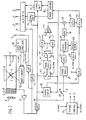
- a color imaging apparatus includes a color television pickup tube 1 having a pair of vertical and horizontal deflection yokes 2 and 3, and a color stripe filter 4 affixed to the rear of a transparent faceplate 5 of an evacuated envelope 7.
- a photoelectrical conversion target 6 is affixed to the rear of the filter 4.
- a lens 9 focuses an object scene on the surface of the target 6 through the color filter 4.
- a video signal is developed by the photoconductive layer of the conversion target 6 when it is scanned by an electron beam emitted from an electron gun 8 and applied to a preamplifier 11.
- Color filter 4 comprises a plurality of recurrent groups of stripes of a first color Fl (which may be one of the primary colors of blue, green and red), a second color F2 (which is cyan or magenta if Fl is blue, cyan or yellow if Fl is green, or yellow or magenta if Fl is red), and a transparent stripe for passing white light. These stripes have equal width and extend vertically across the target 6 and successively arranged across the horizontal dimension of the target such that the color stripes of each group recyclically occur at intervals T.
- the filter 4 has therefore a spatial frequency inversely proportional to the periodic intervals T.
- a typical example of the color filter 4 is shown in Fig. 2 in which the first color stripes Fl are green and the second color stripes F2 are cyan.
- the color filter may comprise recurrent groups of stripes of red, green and blue of different widths with the groups being arranged at intervals T.
- Light passing through the color filter 4 is optically modulated by the striped color filter pattern and develops an electrostatic image on the conversion target 6 which is read by the electron beam.
- the beam is deflected in a line-by-line rectangular raster scan format by the horizontal and vertical yokes 2 and 3 to which sweep currents are supplied from a deflection circuit 10, which is in turn responsive to horizontal and vertical sync pulses supplied fro a vertical- and horizontal-sync generator 19.
- the first filter stripe Fl is green and the second stripe F2 is cyan as illustrated in Fig. 2.
- the color-multiplexed signal contains (G), (B+G) and (R+B+G) components derived respectively from stripes Fl, F2 and W. Therefore, the video signal S obtained from the target 6 is given by: where,
- phase component ⁇ indicates a phase deviation from the reference phase of the "carrier” and represents the spatial difference between the individual filter stripes within each recurrent group, and the phase component 6 represents a phase deviation attributed to the nonlinearity of the deflection system.
- the output of preamplifier 11 is applied to a low-pass filters 12 and 13 and to a band-pass filter 14.
- Low-pass filter 12 has a cut-off frequency immediately below the carrier frequency f 1 to pass the luminance component of the video signal to a luminance output terminal Y.
- Low-pass filter 13 has a cut-off frequency much lower than the cut-off frequency of filter 12 to pass the baseband of the video signal to a matrix circuit 15, this baseband signal being represented by the first term of Equation 1.
- the "carrier" component of the video signal is represented by the second term of Equation 1, this carrier component being passed through the band-pass filter 14 to first inputs of synchronous detectors 16 and 17.
- band-pass filter 14 is also applied through a mode select switch 20 to a frequency discriminator 21 to allow it to detect frequency variations that occur in a reference carrier that is generated during write mode in a manner as will be described hereinbelow.
- a mode select switch 20 Through an analog-to-digital converter 22 the output of frequency discriminator 21 is applied to a field memory 23.
- Field memory 23 is addressed by an address generator 25 clocked by an oscillator 25.
- Oscillator 25 is of a resettable type in which the oscillator output is reset to a predetermined phase in response to a horizontal sync pulse applied thereto from sync generator 19.
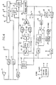
- the color filter 4 includes a horizontal band 30 of alternating opaque and transparent "field” index stripes successively arranged at the same intervals as the color filter stripes of image incident area 32 alongside its upper edge within the rectangular raster area and a vertically extending band 31 of likewise opaque and transparent "line” index stripes arranged at the same intervals as field index stripes 30 alongside the line-start edge of image incident area 32 within the rectangular raster scan area.
- Image pickup tube 1 is preferably provided with a light guide, not shown, to uniformly illuminate the "field” and "line” index stripes 30 and 31 with external light during write and read modes of the field memory 23.
- Field index band 30 is scanned by the electron beam several times to develop a "field” index signal immediately preceding a "field” video signal and the line index band 31 is scanned to develop a "line” index signal immediately preceding each "line” video signal.
- switch 20 is manually turned to "write" position W and the target 6 is illuminated uniformly with light of a predetermined color to generate a "carrier" at frequency f l in addition to the field and line index signals.
- the frequency variations of these signals are detected by frequency discriminator 21 and digitized by A/D converter 22 and written into field memory 23 at a constant rate.
- switch 20 is returned to "read" position R and the target 6 is illuminated with the optical image of an object, producing a color-multiplexed video signal comprising a "carrier” modulated in amplitude with the intensity of picture elements of the image and in phase with the individual stripes of each recurrent group of the filter 4, as represented by the second term of Equation 1.
- the modulated carrier has a phase difference 0 with respect to the reference carrier.
- Target 6 is also illuminated with light rays passing through the field and line index bands 30 and 31 to produce field and line index signals, respectively, as in the write mode.
- Field memory 23 is read at constant rate to supply the stored data to a digital-to-analog converter 26 whose output is coupled to an adder 27.
- variable frequency oscillator 28 responds to the output of field memory 23 via adder 27 by regenerating the field and line index signals and the reference carrier having the same frequency variations as the original.
- the output of variable frequency oscillator 28 is applied to a variable phase shifter 29 which is responsive to a voltage stored in a sample-and-hold circuit 40 to control the phase of the output of oscillator 29 so that it synchronizes with the output of target 6.
- Frequency difference between the field index signal from band-pass filter 14 and the regenerated field index signal from variable phase shifter 29 is detected by frequency comparator 41 at the beginning of each field scan.
- the frequency comparator 41 includes a frequency discriminator 42 which takes an input signal selectively from the output of band-pass filter 14 and the output of variable phase shifter 29 via an electronic switch 43 and supplies its output through an electronic switch 44 selectively to sample-and-hold circuits 45 and 46.
- Electronic switches 43 and 44 are supplied with horizontal sync pulses from sync generator 19 to cause the frequency discriminator 42 to detect the frequency variations of the alternately applied input signals during the time the field index stripes 30 are scanned.
- Sample-and-hold circuits 45 and 46 are supplied with a vertical "window" pulse V from a timing control circuit 50 which is timed to sample the frequency variations of field index signal fed from the band-pass filter 14 and sample the frequency variations of the regenerated field index signal fed from variable phase shifter 29.
- sample-and-holds 45 and 46 respectively store the frequency variations of the field index signals supplied from target 6 and variable phase shifter 29 until the end of the field scan.
- a differential amplifier 47 compares the frequency variations stored in sample-and-holds 45 and 46 and supplies an error voltage to adder 27. This error voltage represents a difference in frequency between the two field index signals.
- This frequency error signal is advantageously used during the following field scan to control the variable frequency oscillator 28 to prevent undesirable asynchronism which might occur between the reference and modulated "carriers" in the event that the carrier component is lost when the incident image is wholly or partially dark.
- Phase difference between the line index signal from band-pass filter 14 and the regenerated line index signal from variable phase shifter 29 is detected by a phase comparator 48 and stored into the sample-and-hold 40 in response to a horizontal "window" pulse H supplied from timing control circuit 50.
- Variable phase shifter 29 is responsive to the detected phase difference at the beginning of each line scan to establish a proper phase relationship with the modulated carrier from band-pass filter 14.
- the reference carrier thus generated is represented by sin(wt + 6).
- sample-and-hold circuits 45 and 46 can be replaced with RC (resistor-capacitor) networks to utilize the frequency variations continuously detected throughout the field scan as a frequency control signal for the variable frequency oscillator 28.
- RC resistor-capacitor
- phase shifter 18 The reference carrier from variable phase shifter 29 is applied to phase shifter 18 where it is shifted in phase by +60° and -60° with respect to the modulated "carrier" and applied respectively to synchronous detectors 16 and 17.
- Color difference signals are produced by the synchronous detectors 16 and 17 and applied to color matrix circuit 15 where they are combined with the baseband of the color-multiplexed signal from low-pass filter 13 to generate primary color signals.
- the nonlinearity indicating frequency variations are derived by a phase-locked loop essentially formed by the phase comparator 48, field memory 23, variable frequency oscillator 28 and variable phase shifter 29.
- the input of A/D converter 22 is taken from phase comparator 48.
- write mode switch 51 is turned to the write position W to supply the output of A/D converter 22 to D/A converter 26 to control the variable frequency oscillator 28 with the phase difference detected by phase comparator 48, while the target 6 is being illuminated uniformly by the reference light as mentioned above.
- a switch 52 is turned to the write position W to disconnect the output of differential amplifier 47 from adder 27.
- the instantaneous value of the phase difference signal from phase comparator 48 is digitized by A/D converter 22 and stored into field memory 23 at a constant rate as the phase comparison proceeds.
- the output of A/D converter 22 is converted to analog form by D/A converter 26 and drives the variable frequency oscillator 28.
- sample-and-hold 40 is sampled in response to the horizontal window pulse H to reset the variable phase shifter 29 to a proper phase in accordance with the phase difference derived in phase comparator 48 by comparison between the line index signal from target 6 and the output of phase shifter 29.
- the output of phase shifter 29 thus varies with the nonlinearity of the beam deflection system.
- the write mode continues until the memory 23 is filled with a frequency variation signal having a length of at least one field.
- switches 51 and 52 are returned to the read position R to couple the output of field memory 23 to D/A converter 26 and couple the output of differential amplifier 47 to adder 27.
- the operation of the Fig. 4 embodiment during read mode is identical to that of the Fig. 1 embodiment.
Landscapes
- Engineering & Computer Science (AREA)
- Multimedia (AREA)
- Signal Processing (AREA)
- Color Television Image Signal Generators (AREA)
- Video Image Reproduction Devices For Color Tv Systems (AREA)
Applications Claiming Priority (4)
| Application Number | Priority Date | Filing Date | Title |
|---|---|---|---|
| JP230250/84 | 1984-11-02 | ||
| JP59230250A JPS61109393A (ja) | 1984-11-02 | 1984-11-02 | カラ−撮像装置 |
| JP59250895A JPS61128692A (ja) | 1984-11-28 | 1984-11-28 | カラ−撮像装置 |
| JP250895/84 | 1984-11-28 |
Publications (3)
| Publication Number | Publication Date |
|---|---|
| EP0180946A2 true EP0180946A2 (de) | 1986-05-14 |
| EP0180946A3 EP0180946A3 (en) | 1988-08-31 |
| EP0180946B1 EP0180946B1 (de) | 1991-06-19 |
Family
ID=26529232
Family Applications (1)
| Application Number | Title | Priority Date | Filing Date |
|---|---|---|---|
| EP85113989A Expired EP0180946B1 (de) | 1984-11-02 | 1985-11-04 | Farbbildaufnahmeanordnung |
Country Status (2)
| Country | Link |
|---|---|
| EP (1) | EP0180946B1 (de) |
| DE (1) | DE3583279D1 (de) |
Cited By (1)
| Publication number | Priority date | Publication date | Assignee | Title |
|---|---|---|---|---|
| US6633333B1 (en) | 1996-10-02 | 2003-10-14 | Gec-Marconi Ltd. | Cameras |
Family Cites Families (2)
| Publication number | Priority date | Publication date | Assignee | Title |
|---|---|---|---|---|
| JPS5376623A (en) * | 1976-12-17 | 1978-07-07 | Matsushita Electric Ind Co Ltd | Single-tube-type color television camera |
| JPS59153392A (ja) * | 1983-02-22 | 1984-09-01 | Victor Co Of Japan Ltd | カラ−撮像装置 |
-
1985
- 1985-11-04 EP EP85113989A patent/EP0180946B1/de not_active Expired
- 1985-11-04 DE DE8585113989T patent/DE3583279D1/de not_active Expired - Fee Related
Cited By (1)
| Publication number | Priority date | Publication date | Assignee | Title |
|---|---|---|---|---|
| US6633333B1 (en) | 1996-10-02 | 2003-10-14 | Gec-Marconi Ltd. | Cameras |
Also Published As
| Publication number | Publication date |
|---|---|
| EP0180946A3 (en) | 1988-08-31 |
| EP0180946B1 (de) | 1991-06-19 |
| DE3583279D1 (de) | 1991-07-25 |
Similar Documents
| Publication | Publication Date | Title |
|---|---|---|
| NL8100902A (nl) | Stelsel voor het corrigeren van alle met het raster samenhangende fouten in beeldopname-organen in een televisiecamera. | |
| US4595954A (en) | Image signal reproduction circuit for solid-state image sensor | |
| CA1211207A (en) | Color image pickup apparatus | |
| EP0180131B1 (de) | Farbabbildungsvorrichtung mit Trägerverlustausgleich | |
| US2827512A (en) | Color television camera | |
| EP0004474B1 (de) | Verfahren und Einrichtung zur Verarbeitung von Farbsignalen | |
| EP0178130B1 (de) | Bildaufnahmeeinrichtung mit Ausgleichung der durch Änderungen der Abtastungsgeschwindigkeit verursachten Phasefehlern | |
| EP0180946B1 (de) | Farbbildaufnahmeanordnung | |
| US3828121A (en) | Color signal producing system utilizing spatial color encoding and comb filtering | |
| GB2032216A (en) | Flying spot continuous motion telecine apparatus having variable line frequency | |
| US4185296A (en) | Color television camera | |
| US4160265A (en) | Vertical aperture correction circuit | |
| EP0179339B1 (de) | Farbabbildungsvorrichtung mit Frequenzverhältnis 1:2 zwischen Video- und Referenzsignalen für Farbdemodulation mit hohem Störabstand | |
| US3840696A (en) | Single tube color television camera with recovery of index signal for elemental color component separation | |
| US3745237A (en) | Color television camera equipment having a reference filter and a color filter assembly interposed between the camera and subject | |
| EP0274820B1 (de) | Farbfernsehkamera | |
| US2938076A (en) | Circuits embodying television pick-up tubes | |
| US3647947A (en) | Chrominance signal generator having a patterned filter | |
| JPS6188685A (ja) | カラ−撮像装置 | |
| US3757033A (en) | Shadowing system for color encoding camera | |
| US4811088A (en) | Color video camera apparatus providing correction of light intensity-dependent phase errors in color multiplex carrier signal | |
| US4857995A (en) | Color imaging apparatus including control system for stabilizing phase and frequency of a video signal carrier frequency | |
| JPH0195685A (ja) | カラー撮像装置 | |
| US4668976A (en) | Radiation resistant color television camera | |
| US3754096A (en) | Color television signal reproducing system |
Legal Events
| Date | Code | Title | Description |
|---|---|---|---|
| PUAI | Public reference made under article 153(3) epc to a published international application that has entered the european phase |
Free format text: ORIGINAL CODE: 0009012 |
|
| AK | Designated contracting states |
Kind code of ref document: A2 Designated state(s): DE FR GB |
|
| PUAL | Search report despatched |
Free format text: ORIGINAL CODE: 0009013 |
|
| AK | Designated contracting states |
Kind code of ref document: A3 Designated state(s): DE FR GB |
|
| 17P | Request for examination filed |
Effective date: 19881216 |
|
| 17Q | First examination report despatched |
Effective date: 19901008 |
|
| GRAA | (expected) grant |
Free format text: ORIGINAL CODE: 0009210 |
|
| AK | Designated contracting states |
Kind code of ref document: B1 Designated state(s): DE FR GB |
|
| ET | Fr: translation filed | ||
| REF | Corresponds to: |
Ref document number: 3583279 Country of ref document: DE Date of ref document: 19910725 |
|
| PLBE | No opposition filed within time limit |
Free format text: ORIGINAL CODE: 0009261 |
|
| STAA | Information on the status of an ep patent application or granted ep patent |
Free format text: STATUS: NO OPPOSITION FILED WITHIN TIME LIMIT |
|
| 26N | No opposition filed | ||
| PGFP | Annual fee paid to national office [announced via postgrant information from national office to epo] |
Ref country code: GB Payment date: 19921026 Year of fee payment: 8 |
|
| PGFP | Annual fee paid to national office [announced via postgrant information from national office to epo] |
Ref country code: FR Payment date: 19921109 Year of fee payment: 8 |
|
| PGFP | Annual fee paid to national office [announced via postgrant information from national office to epo] |
Ref country code: DE Payment date: 19921123 Year of fee payment: 8 |
|
| PG25 | Lapsed in a contracting state [announced via postgrant information from national office to epo] |
Ref country code: GB Effective date: 19931104 |
|
| GBPC | Gb: european patent ceased through non-payment of renewal fee |
Effective date: 19931104 |
|
| PG25 | Lapsed in a contracting state [announced via postgrant information from national office to epo] |
Ref country code: FR Effective date: 19940729 |
|
| PG25 | Lapsed in a contracting state [announced via postgrant information from national office to epo] |
Ref country code: DE Effective date: 19940802 |
|
| REG | Reference to a national code |
Ref country code: FR Ref legal event code: ST |