EP0177465A2 - Verfahren und Gerät zum Bearbeiten von kompandierten PCM-Sprachdaten - Google Patents
Verfahren und Gerät zum Bearbeiten von kompandierten PCM-Sprachdaten Download PDFInfo
- Publication number
- EP0177465A2 EP0177465A2 EP85850259A EP85850259A EP0177465A2 EP 0177465 A2 EP0177465 A2 EP 0177465A2 EP 85850259 A EP85850259 A EP 85850259A EP 85850259 A EP85850259 A EP 85850259A EP 0177465 A2 EP0177465 A2 EP 0177465A2
- Authority
- EP
- European Patent Office
- Prior art keywords
- rom
- signal
- parallel
- signals
- serial
- Prior art date
- Legal status (The legal status is an assumption and is not a legal conclusion. Google has not performed a legal analysis and makes no representation as to the accuracy of the status listed.)
- Withdrawn
Links
Images

Classifications
-
- H—ELECTRICITY
- H04—ELECTRIC COMMUNICATION TECHNIQUE
- H04M—TELEPHONIC COMMUNICATION
- H04M3/00—Automatic or semi-automatic exchanges
- H04M3/42—Systems providing special services or facilities to subscribers
- H04M3/56—Arrangements for connecting several subscribers to a common circuit, i.e. affording conference facilities
- H04M3/561—Arrangements for connecting several subscribers to a common circuit, i.e. affording conference facilities by multiplexing
Definitions
- Digitized voice data is "companded” to 8 bits for transmission in bandwidth limited networks.
- Several algorithms are commercially used to perform the "companding" function, but regardless of the exact transformation function used, the eight bit result is a floating point number--i.e., mantissa plus exponent.
- the method and apparatus of the present invention permits a plurality of parties to speak to each other on a conference line with a minimum of interference.
- Each of the parties has a headset provided with a microphone and receiver.
- ADC analog-to-digital converter
- the audio signal is first converted by an analog-to-digital converter (ADC) to an eight-bit digital signal, which is then fed to a parallel-to-serial converter which converts the signal to a serial PCM companded wave train.
- ADC analog-to-digital converter
- This serial PCM wave train is then transmitted to a remote location over a single wire.
- Upon receiving the serial PCM signal it is first fed to a serial-to-parallel converter which converts the signal back to an eight-bit parallel signal, which is fed to one input of a pre-programmed ROM.
- This eight-bit signal provides one-half of the sixteen-bit address for a lookup ROM.
- the other half of the sixteen-bit ROM address is supplied by another subscriber over an indentical circuit as described above. If it is desired to add more subscribers, the address is widened or a plurality of sequential lookups are performed.
- the output of the ROM is an eight-bit companded parallel signal that is, in turn, fed to a parallel-to-serial converter for being converted back to a serial PCM signal to be transmitted over a line to a second serial-to-parallel converter. The latter converts the signal back to an eight-bit parallel signal which is fed to a digital-to-analog converter (DAC) whose output, in turn, is fed to a receiver to reproduce the audio signal.
- DAC digital-to-analog converter
- the ROM Prior to operating the system, the ROM is pre- programmed to contain all possible combinations of results as defined by the two eight-bit inputs from the A and B subscribers. It is to be understood, of course, that when more than two subscribers are used,the ROM is pre-programmed to handle all possible combinations. For two subscribers there are 2 16 possible combinations prestored in the ROM for handling all possible combinations of teh two eight-bit signals coming in from the A and B subscribers. A similar circuit is used for transmitting the conversation back from the ultimate receiver to the parties tied in on the lines.
- a simplified circuit may be used for receiving the inputs from the subscribers A and B. These two inputs are fed to a sign ROM, a sum ROM and a delta ROM.
- the sign ROM is pre-programmed to determine the output sign and whether the remainder of the output data is derived from the sum ROM or the delta ROM. In other words the sign ROM only says whether the information should be taken from the sum ROM or the delta ROM, and produces a sign output indicating the sign of the eight-bit signal.
- the sign ROM is also used to enable the sum ROM and the delta ROM to produce a seven-bit output from the appropriate ROM.
- the use of the sum and delta ROMs eliminates the redundancy of the stored data in the ROM and, therefore, reduces the storage requirement.
- a multiplier ROM may also be inserted in the circuit between the first serial-to-parallel converter and the ROM for multiplying the signal to provide volume control for the circuit.
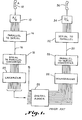
- ADC 10 is connected to the transmitting portion or microphone of a telephone headset 12 for converting the voice signals to an eight-bit parallel digital signal.
- These parallel digital signals are, in turn, converted by a parallel-to-serial converter 14 for transmission over long distances over a single line 16. It is not practical to transmit the signals in parallel form over long distances.
- the serial PCM signal transmitted over the line 16 is then converted back to an eight-bit parallel companded signal by a serial-to-parallel converter 18.
- This eight-bit companded digital signal is fed to a linearizer 20 which converts it to a twelve-bit linear digital data signal. The reason for this is that you cannot add a floating point number to another floating point number in conventional adders.
- the twelve-bit linear digital signal is then fed into one input of a digital adder 22 to be added with a similar twelve-bit linear digital data signal coming from another headset B. It is to be understood that any number of headsets can be fed into the digital adder.
- the digital adder performs a mathematical adding process and produces a thirteen-bit sum on its output terminals in parallel form. This thirteen-bit sum is then fed to a delinearizer 26 which converts the signal back to an eight-bit companded digital data signal in parallel form that is fed to a parallel-to-serial converter 28.
- the latter converts the eight-bit companded data signal back to a serial PCM signal for transmission over a long line 30 to another serial-to-parallel converter 32, which feeds the parallel data to a DAC 34 associated with the receiver portion of a headset 36.
- a serial PCM signal for transmission over a long line 30 to another serial-to-parallel converter 32, which feeds the parallel data to a DAC 34 associated with the receiver portion of a headset 36.
- the circuit shown in Figure 2 has been developed.
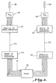
- the audio signal from the headset 38 is fed directly to an ADC 40 which converts the signal to an eight-bit parallel digital signal.
- the latter is fed to a parallel-to-serial converter 42 which converts the signal to a serial PCM companded wave train, which is transmitted over long distance wire 44.
- the received serial PCM signal is first fed to a serial-to-parallel converter 46 which converts it back to an eight-bit parallel data signal, in turn fed to one input of a lookup ROM 48.
- This eight-bit signal provides one-half of a sixteen-bit address for ROM 48.
- the other half of the address is supplied by another subscriber identified by B. If it is desirable to add more subscribers, then one would merely make multiple lookup steps or make the address wider.
- the output of the ROM 48 is an eight-bit companded parallel signal that is fed to a second parallel-to-serial converter 50 for conversion back to a serial PCM signal transmitted over a line 52 to another serial-to-parallel converter 54. The latter converts the signal back to an eight-bit parallel signal that is fed to a DAC 56 whose output is coupled to a receiver handset 58.
- the ROM 48 Prior to operating the system, the ROM 48 is pre- programmed to contain all possible combinations of results as defined by the two eight-bit input quantities from the A and B subscribers. That is, the ROM 48 is programmed to represent on its output the instantaneous sum of the two digital input qualities. These two digital input qualities represent an audio sample of the signals produced by both the A and B. subscribers. As can be seen, such represents a large amount of storage and in normal implementation, shortcuts are taken to minimize the amount of storage required for the ROM.
- FIG. 3 One such circuit is shown in Figure 3, Wherein two inputs are received from subscribers A and B. These two inputs are fed to a sign ROM 60, a sum ROM 62, and a delta ROM 64.
- the sign ROM 60 is a 64K times 2-bit ROM which has been programmed to determine the output sign and whether the remainder of the output data is derived from the sum ROM 62 or the delta ROM 64. In other words, the sign ROM 60 only says whether the information should be taken from the sum ROM 62 or the delta ROM 64 and produces a sign output on lead 66 indicating the sign of the eight-bit signal.
- Either the sum ROM 62 or delta ROM 64 enabled by the signal coming in over lead 68 will output seven bits of resulting data onto the output line 70.
- the use of the sum ROM 62 and the delta ROM 64 eliminates the redundancy of the stored data and, therefore, reduces the storage requirement. This is accomplished by connecting an output lead 68 from the sign ROM 60 to an enable input of both a sum ROM 62 and a delta ROM 64.
- the sum ROM 62 has the sum programs stored therein for summing all positive and all negative programs whereas the delta ROM has all the differences stored therein.
- the incoming data from the serial-to-parallel converter 46 produced by the A and B subscribers determines what location is being read from and the respective ROM 62 and 64.
- the circuit of Figure 4 can be inserted in the system for controlling the volume level.
- This circuit includes a multiplier ROM connected between the serial-to-parallel converter 46 and the ROM memory 48 for multiplying the signal for providing a volume control for the circuit.
- a multiplier ROM connected between the serial-to-parallel converter 46 and the ROM memory 48 for multiplying the signal for providing a volume control for the circuit.
- the remaining seven data bits are applied to ROM 76 as part of a thirteen-bit address.
- the other six bits of address are derived from a multiplier con- stand input lead 78 and determine the multiplication constant that will be applied to the output data which appears on line 80.
- the output line 80 is, in turn, fed directly into the ROM 48. This enables the amplitude of the different scribers to
Applications Claiming Priority (2)
| Application Number | Priority Date | Filing Date | Title |
|---|---|---|---|
| US06/655,601 US4588986A (en) | 1984-09-28 | 1984-09-28 | Method and apparatus for operating on companded PCM voice data |
| US655601 | 1984-09-28 |
Publications (2)
| Publication Number | Publication Date |
|---|---|
| EP0177465A2 true EP0177465A2 (de) | 1986-04-09 |
| EP0177465A3 EP0177465A3 (de) | 1987-12-16 |
Family
ID=24629565
Family Applications (1)
| Application Number | Title | Priority Date | Filing Date |
|---|---|---|---|
| EP85850259A Withdrawn EP0177465A3 (de) | 1984-09-28 | 1985-08-16 | Verfahren und Gerät zum Bearbeiten von kompandierten PCM-Sprachdaten |
Country Status (6)
| Country | Link |
|---|---|
| US (1) | US4588986A (de) |
| EP (1) | EP0177465A3 (de) |
| JP (1) | JPS6188646A (de) |
| AU (1) | AU564685B2 (de) |
| CA (1) | CA1235541A (de) |
| IL (1) | IL76051A (de) |
Cited By (1)
| Publication number | Priority date | Publication date | Assignee | Title |
|---|---|---|---|---|
| EP0613282A1 (de) * | 1993-02-23 | 1994-08-31 | Siemens Aktiengesellschaft | Schaltungsanordnung zur Herstellung von Konferenzverbindungen in einer digitalen Zeitmultiplex-Fernmeldevermittlungsstelle |
Families Citing this family (12)
| Publication number | Priority date | Publication date | Assignee | Title |
|---|---|---|---|---|
| US4870685A (en) * | 1986-10-26 | 1989-09-26 | Ricoh Company, Ltd. | Voice signal coding method |
| US5038143A (en) * | 1987-12-09 | 1991-08-06 | Texas Instruments Incorporated | Analog interface system |
| US4903240A (en) * | 1988-02-16 | 1990-02-20 | Tektronix, Inc. | Readout circuit and method for multiphase memory array |
| US4975880A (en) * | 1988-05-02 | 1990-12-04 | Tektronix, Inc. | Memory system for storing data from variable numbers of input data streams |
| JPH084531B2 (ja) * | 1989-09-27 | 1996-01-24 | 株式会社イトーキクレビオ | 電動式移動棚 |
| JPH04275890A (ja) * | 1991-03-04 | 1992-10-01 | Matsushita Electric Ind Co Ltd | 多連ハンド装置 |
| US5576980A (en) * | 1991-06-28 | 1996-11-19 | Texas Instruments Incorporated | Serializer circuit for loading and shifting out digitized analog signals |
| US5237591A (en) * | 1991-08-19 | 1993-08-17 | At&T Bell Laboratories | Circuit for digitally adding loss to a signal |
| US5696879A (en) * | 1995-05-31 | 1997-12-09 | International Business Machines Corporation | Method and apparatus for improved voice transmission |
| DE19643872A1 (de) * | 1996-10-31 | 1998-05-07 | Alsthom Cge Alcatel | Optische Netzabschlußeinheit eines hybriden Glasfaser-Koaxialkabel-Zugangsnetzes |
| US5986596A (en) * | 1997-10-24 | 1999-11-16 | 3Com Corporation | Concise storage and expansion of signal constellations in PCM space for high speed data communication |
| KR101594866B1 (ko) * | 2009-06-02 | 2016-02-26 | 엘에스산전 주식회사 | 전원 차단 시스템용 병렬 디지털 신호의 직렬 디지털 신호로의 변환 장치 및 방법 |
Citations (4)
| Publication number | Priority date | Publication date | Assignee | Title |
|---|---|---|---|---|
| US4301531A (en) * | 1979-07-02 | 1981-11-17 | Motorola, Inc. | Three-party conference circuit for digital time-division-multiplex communication systems |
| US4313174A (en) * | 1980-03-17 | 1982-01-26 | Rockwell International Corporation | ROM-Based parallel digital arithmetic device |
| GB2109135A (en) * | 1981-11-09 | 1983-05-25 | Rca Corp | Digital signal processing |
| FR2533784A1 (fr) * | 1982-09-28 | 1984-03-30 | Thomson Csf Mat Tel | Dispositif de conferences multiples pour autocommutateur temporel mic avec reseau de connexion |
Family Cites Families (5)
| Publication number | Priority date | Publication date | Assignee | Title |
|---|---|---|---|---|
| US4230908A (en) * | 1979-01-22 | 1980-10-28 | Plessey Canada Limited | Telephone summing circuit |
| GB2059123B (en) * | 1979-09-22 | 1983-09-21 | Kokusai Denshin Denwa Co Ltd | Pcm signal calculator |
| CA1151327A (en) * | 1981-06-08 | 1983-08-02 | Ernst A. Munter | Digital conference circuit and method |
| JPH0646754B2 (ja) * | 1983-02-21 | 1994-06-15 | 株式会社日立製作所 | レベル制御会議通話方式 |
| JPS59153370A (ja) * | 1983-02-21 | 1984-09-01 | Hitachi Ltd | 会議通話制御方式 |
-
1984
- 1984-09-28 US US06/655,601 patent/US4588986A/en not_active Expired - Fee Related
-
1985
- 1985-07-30 CA CA000487815A patent/CA1235541A/en not_active Expired
- 1985-08-07 AU AU45865/85A patent/AU564685B2/en not_active Ceased
- 1985-08-09 IL IL76051A patent/IL76051A/xx unknown
- 1985-08-16 EP EP85850259A patent/EP0177465A3/de not_active Withdrawn
- 1985-08-23 JP JP60185651A patent/JPS6188646A/ja active Pending
Patent Citations (4)
| Publication number | Priority date | Publication date | Assignee | Title |
|---|---|---|---|---|
| US4301531A (en) * | 1979-07-02 | 1981-11-17 | Motorola, Inc. | Three-party conference circuit for digital time-division-multiplex communication systems |
| US4313174A (en) * | 1980-03-17 | 1982-01-26 | Rockwell International Corporation | ROM-Based parallel digital arithmetic device |
| GB2109135A (en) * | 1981-11-09 | 1983-05-25 | Rca Corp | Digital signal processing |
| FR2533784A1 (fr) * | 1982-09-28 | 1984-03-30 | Thomson Csf Mat Tel | Dispositif de conferences multiples pour autocommutateur temporel mic avec reseau de connexion |
Cited By (2)
| Publication number | Priority date | Publication date | Assignee | Title |
|---|---|---|---|---|
| EP0613282A1 (de) * | 1993-02-23 | 1994-08-31 | Siemens Aktiengesellschaft | Schaltungsanordnung zur Herstellung von Konferenzverbindungen in einer digitalen Zeitmultiplex-Fernmeldevermittlungsstelle |
| US5511071A (en) * | 1993-02-23 | 1996-04-23 | Siemens Aktiengesellschaft | Circuit arrangement for setting up conference calls in a digital time-division multiplex telecommunications switching center |
Also Published As
| Publication number | Publication date |
|---|---|
| IL76051A0 (en) | 1985-12-31 |
| JPS6188646A (ja) | 1986-05-06 |
| CA1235541A (en) | 1988-04-19 |
| EP0177465A3 (de) | 1987-12-16 |
| US4588986A (en) | 1986-05-13 |
| AU564685B2 (en) | 1987-08-20 |
| IL76051A (en) | 1989-02-28 |
| AU4586585A (en) | 1986-04-10 |
Similar Documents
| Publication | Publication Date | Title |
|---|---|---|
| US5533112A (en) | Volume control in digital teleconferencing | |
| US4588986A (en) | Method and apparatus for operating on companded PCM voice data | |
| US5034947A (en) | Whisper circuit for a conference call bridge including talker nulling and method therefor | |
| US5054021A (en) | Circuit for nulling the talker's speech in a conference call and method thereof | |
| US5020098A (en) | Telephone conferencing arrangement | |
| JP3306797B2 (ja) | 量子化雑音抑制方法、ディジタルモデムおよび通信方法 | |
| US4339818A (en) | Digital multiplexer with increased channel capacity | |
| US4829514A (en) | Digital voice recording and reproduction and telephone network signalling using direct storage in RAM of PCM encoded data | |
| JPS6253589A (ja) | デイジタル信号プロセツサ | |
| EP0066947A1 (de) | Mit aufeinanderfolgenden Rahmen arbeitender digitaler Multiflexer mit erhöhter Kanalkapazität | |
| US4126766A (en) | 3-Port conference circuit for use in private automatic branch exchange | |
| GB1576520A (en) | Signal transmission system | |
| US4048449A (en) | Method for forming a conference connection in a telecommunication switching system | |
| JPS6159019B2 (de) | ||
| US4845497A (en) | Conference circuit for a digital communication system | |
| JPH0337772B2 (de) | ||
| US4757493A (en) | Multi-party telephone conferencing apparatus | |
| US4677610A (en) | Three-port conference circuit for use in a digital telephone system | |
| JPS5853537B2 (ja) | 時分割通話路割込方式 | |
| US4493949A (en) | Parallel operation of telephone equipment on a digital loop | |
| US6522739B1 (en) | Apparatus and method for multi-access conference call in exchange system | |
| CN218734481U (zh) | 一种基于aes67网关的视频会议传输转换装置 | |
| JP2670283B2 (ja) | 補助伝送路伝送方式 | |
| CA1153137A (en) | Parallel operation of telephone equipment on a digital loop | |
| JPS5866440A (ja) | 波形符号化方式 |
Legal Events
| Date | Code | Title | Description |
|---|---|---|---|
| PUAI | Public reference made under article 153(3) epc to a published international application that has entered the european phase |
Free format text: ORIGINAL CODE: 0009012 |
|
| 17P | Request for examination filed |
Effective date: 19850821 |
|
| AK | Designated contracting states |
Kind code of ref document: A2 Designated state(s): BE CH DE FR GB IT LI NL SE |
|
| PUAL | Search report despatched |
Free format text: ORIGINAL CODE: 0009013 |
|
| AK | Designated contracting states |
Kind code of ref document: A3 Designated state(s): BE CH DE FR GB IT LI NL SE |
|
| 17Q | First examination report despatched |
Effective date: 19900502 |
|
| STAA | Information on the status of an ep patent application or granted ep patent |
Free format text: STATUS: THE APPLICATION IS DEEMED TO BE WITHDRAWN |
|
| 18D | Application deemed to be withdrawn |
Effective date: 19900913 |
|
| RIN1 | Information on inventor provided before grant (corrected) |
Inventor name: BYRNE, FRANK |