EP0176314A2 - Röntgen-Anordnung - Google Patents
Röntgen-Anordnung Download PDFInfo
- Publication number
- EP0176314A2 EP0176314A2 EP85306633A EP85306633A EP0176314A2 EP 0176314 A2 EP0176314 A2 EP 0176314A2 EP 85306633 A EP85306633 A EP 85306633A EP 85306633 A EP85306633 A EP 85306633A EP 0176314 A2 EP0176314 A2 EP 0176314A2
- Authority
- EP
- European Patent Office
- Prior art keywords
- detector
- radiation
- elements
- circuitry
- detector array
- Prior art date
- Legal status (The legal status is an assumption and is not a legal conclusion. Google has not performed a legal analysis and makes no representation as to the accuracy of the status listed.)
- Granted
Links
- 238000002601 radiography Methods 0.000 title claims abstract description 20
- 230000005855 radiation Effects 0.000 claims abstract description 48
- 230000007246 mechanism Effects 0.000 claims abstract description 4
- 238000005070 sampling Methods 0.000 claims description 45
- 230000004044 response Effects 0.000 claims description 7
- 238000012545 processing Methods 0.000 claims description 6
- 230000001419 dependent effect Effects 0.000 claims description 2
- 230000008901 benefit Effects 0.000 description 11
- 238000000034 method Methods 0.000 description 11
- 238000003384 imaging method Methods 0.000 description 5
- 230000006872 improvement Effects 0.000 description 5
- 230000010354 integration Effects 0.000 description 4
- 230000004304 visual acuity Effects 0.000 description 4
- 239000011159 matrix material Substances 0.000 description 3
- 230000009467 reduction Effects 0.000 description 3
- 238000012546 transfer Methods 0.000 description 3
- 230000000007 visual effect Effects 0.000 description 3
- 238000003491 array Methods 0.000 description 2
- 230000003111 delayed effect Effects 0.000 description 2
- 230000002708 enhancing effect Effects 0.000 description 2
- 230000003287 optical effect Effects 0.000 description 2
- 230000008569 process Effects 0.000 description 2
- OAICVXFJPJFONN-UHFFFAOYSA-N Phosphorus Chemical compound [P] OAICVXFJPJFONN-UHFFFAOYSA-N 0.000 description 1
- 238000009825 accumulation Methods 0.000 description 1
- 238000007792 addition Methods 0.000 description 1
- 238000004458 analytical method Methods 0.000 description 1
- 230000002238 attenuated effect Effects 0.000 description 1
- 230000015556 catabolic process Effects 0.000 description 1
- 239000004020 conductor Substances 0.000 description 1
- 230000007423 decrease Effects 0.000 description 1
- 238000006731 degradation reaction Methods 0.000 description 1
- 230000001934 delay Effects 0.000 description 1
- 238000012217 deletion Methods 0.000 description 1
- 230000037430 deletion Effects 0.000 description 1
- 238000013461 design Methods 0.000 description 1
- 238000001514 detection method Methods 0.000 description 1
- 238000002059 diagnostic imaging Methods 0.000 description 1
- 230000002349 favourable effect Effects 0.000 description 1
- 238000012423 maintenance Methods 0.000 description 1
- 238000012986 modification Methods 0.000 description 1
- 230000004048 modification Effects 0.000 description 1
- 229910021420 polycrystalline silicon Inorganic materials 0.000 description 1
- 229920005591 polysilicon Polymers 0.000 description 1
- 238000009877 rendering Methods 0.000 description 1
- 238000012552 review Methods 0.000 description 1
- 238000000926 separation method Methods 0.000 description 1
- 238000012163 sequencing technique Methods 0.000 description 1
- 239000007787 solid Substances 0.000 description 1
Images


Classifications
-
- G—PHYSICS
- G01—MEASURING; TESTING
- G01T—MEASUREMENT OF NUCLEAR OR X-RADIATION
- G01T1/00—Measuring X-radiation, gamma radiation, corpuscular radiation, or cosmic radiation
- G01T1/16—Measuring radiation intensity
- G01T1/161—Applications in the field of nuclear medicine, e.g. in vivo counting
- G01T1/164—Scintigraphy
- G01T1/166—Scintigraphy involving relative movement between detector and subject
-
- A—HUMAN NECESSITIES
- A61—MEDICAL OR VETERINARY SCIENCE; HYGIENE
- A61B—DIAGNOSIS; SURGERY; IDENTIFICATION
- A61B6/00—Apparatus or devices for radiation diagnosis; Apparatus or devices for radiation diagnosis combined with radiation therapy equipment
- A61B6/06—Diaphragms
Definitions
- This invention relates to radiography systems.
- Radiography is a long known medical diagnostic imaging technique.
- a radiation source e.g. an x-ray source
- a radiation source e.g. an x-ray source
- a cassette containing an x-ray sensitive phosphor screen and light and x-ray sensitive film is positioned in the x-ray path on the side of the patient opposite the source.
- X-radiation passing through the patient's body is attenuated to produce a shadow image of a portion of the patient through which the x-rays pass.
- digital radiographic techniques and systems have been developed.
- the source directs x-radiation through a patient's body to a detector assembly located in the beam path beyond the patient.
- the detector produces electrical signals defining the radiation pattern emergent from the patient. These signals are then processed to yield a visual display of the image.
- the detector assembly includes an elongated array of individual discrete detector elements. Each detector element responds to incident x-radiation to produce an analogue electrical charge signal indicative of such radiation. These analog electrical signals represent the radiation pattern or image emergent from the patient's body and incident on the detector array.
- the analog signals are sampled and processed by imaging circuitry, primarily to improve their signal to noise ratio, and are subsequently digitized.
- the digital signals are fed to a digital data processing unit (DPU).
- the data processing unit records and/or processes and enhances the digital data.
- a display unit responds to appropriate digital data representing the image to convert the digital information back into analog form and to produce a visual display of the patient's internal body structure derived from the acquired image pattern of radiation.
- the display unit can be coupled directly to the digital data processing unit for substantially real time imaging, or can be fed stored digital data from digital storage means such as tapes or disks representing patient images produced from earlier studies.
- Digital radiography includes techniques in which a thin spread beam of x-radiation is used.
- SPR scan projection radiography
- the spread beam is scanned across the patient, or the patient is movably interposed between the spread beam X-ray source and the detector assembly, the detector being maintained in continuous alignment with the beam.
- the relative movement effected between the source-detector arrangement and the patient's body scans a large portion of the body.
- Discrete element detectors have been proposed comprising a single line of detector elements. Other proposals have included rectangular detector arrays of square detector elements.
- the detector array comprises a rectangular array of square detector elements
- TDI time delay and integrate
- the detector element ouput signals are sampled at successive increments of detector movement equal to the length of a side of a single detector element.
- the spatial resolution of a rectangular detector array when used with TDI as described above is poorer than the maximum inherently obtainable resolution.
- MTF modulation transfer function
- a rectangular detector element has an MTF in each of the x and y co-ordinates of its energy receiving face.
- MTF X MTFy
- This first zero is generally taken as representing the maximum spatial frequency (detail) which a square detector element can reliably image.
- This phenonemon is one limiting factor on the resolving capability of any square detector, and is dependent upon its size, or "aperture”. This parameter is referred to as the "aperture cutoff frequency”.
- a detector element is also limited by another resolution constraint known as the "Nyquist frequency".
- the Nyquist frequency is a spatial frequency above which the detector element cannot resolve separate lines. Rather than being a function of the detector size, however, the Nyquist frequency is related to the incremental distance at which successive samplings of the detector element output signal occur.
- the Nyquist cutoff frequency is relevant since the use of TDI circuitry requires repeated detector output samplings.
- the Nyquist criterion is also applicable in the y coordinate of a rectangular array.
- the equivalent sampling distance between adjancent rows of square elements is the length p of one side of an element.
- a radiography system embodying the present invention includes a radiation source and a detector array spaced sufficiently from the source to accommodate the placement of a body between the source and the detector.
- Mechanism is provided for scanning the detector array relative to a body while aligned with the radiation source.
- Power means is employed for actuating the source to direct radiation through the body and toward the detector array during scanning.
- the array comprises a number of detector elements each responsive to incident radiation to produce electrical signals indicative of the radiaton. Circuitry coupled to the detector array responds to these signals to generate an image depicting internal structure of the body as evidenced by a radiation pattern emergent from the body and incident on the detector array.
- the detector array comprises a plurality of individual detector elements, arranged in a pattern of staggered columns, the array being scanned in a direction substantially perpendicular to the columns.
- the staggered nature of the detector element columns geometrically reduces the effective sampling distance between adjacent rows of detector elements to an amount equal to 1/2 the dimension of a single detector element taken in a direction along the columns. This phenomenon results because of a specific aspect of the invention wherein each staggered column of elements is displaced from adjacent columns by an amount equal to 1/2 the dimension of a single detector element along the column. This configuration results in a pattern wherein adjacent rows of detector elements are partially interspersed with one another.
- This geometry improves the resolving capability of the detector array in the y direction (parallel to the columms) to the limit of its resolving power as dictated by the aperture cutoff frequency determined by element size.
- the geometry modifies the Nyquist frequency of the detector in the y direction to a value which is substantially coincident with the aperture cutoff frequency, rather than permitting a Nyquist frequency more limiting in resolution than the aperture cutoff criterion.
- the TDI circuitry samples detector element outputs at successive increments of detector motion equal tc 1/2 the width of a single detector element in a direction perpendicular to the column, i.e., parallel to the dttector element rows. This actual reduction in sampling distance improves the Nyquist frequency in the x direction, rendering it substantially equal to the aperture cutoff frequency, so that the Nyquist frequency does not limit resolution to a level poorer than that permitted by the aperture cutoff limitation.
- a more specific feature of the invention resides in the use of individual detector elements having a substantially uniform square cross-section.
- the use of such square elements (as opposed to circular elements, for example) facilitates obtaining the maximum radiation sensitive surface area with respect to a given overall detector assembly size.
- An aspect of the TDI circuitry of this invention resides in that the circuitry must be separate from, rather than integral with, the individual detector elements. This aspect permits the interposition of different delay circuitry in the respective outputs of the individual detector elements.
- delay circuitry is provided such that output signals from each member of a detector element row are delayed, with respect to those of the immediately preceding detector element, as a function of the x direction sampling distance and by the degree of separation of the elements of the row resulting from the interspersion of adjacent rows.
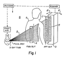
- Figures 1 and 2 illustrate a slit projection type of digital radiography system S in which the present . invention is incorporated.
- the system S scans an X-ray spread beam approximately 1 to 2 centimeters in thickness about a vertical axis across a patient's chest and detects a pattern of X-rays emergent from the patient's body. Information represented by the detected X-rays is processed and displayed to illustrate a representation of an image of the patient's internal body structure or condition.
- the system S includes an X-ray source X affixed to mounting structure M for projecting the spread beam B of X-rays through the body of a patient P, to strike an aligned detector assembly D comprising a plurality of detector elements.
- the spread beam B is confined by a forward slit K to a substantially vertical plane.
- the detector assembly D comprises a generally vertically elongated staggered array of individual detector elements 6 (described in more detail below) and is aligned with the vertical plane defined by the spread beam B.
- An aft slit J attached to the detector assembly D serves to further define the spread beam B.
- the X-ray source X is mounted on the structure M to rotate about a vertical axis, defined in Figure 2 as extending into the plane of the paper.
- Mechanical linkage L couples the X-ray tube X to the detector array D and slits K and J and causes the detector array to scan behind the patient's body along an arcuate path defined by the arrows A, A' in order to maintain the detector assembly D aligned with the beam B throughout the scanning rotative motion of the beam.
- the embodiment of the scanning mechanism is not to be limited to fixed or rigid mechanical linkage connecting the elements to be moved.
- Servo control and associated power drive apparatus embodiments can also be adapted by those of skill in the art to accomplish the desired scanning.
- the X-ray tube X can also be pivoted about its focal spot, to maintain the beam B aligned with the scanning detector.
- the X-ray source X is controlled by power means to emit the spread beam B as either a continuous X-ray beam or a rapid succession of X-ray pulses.
- the X-ray tube X and the detector assembly D synchronously scan, about a vertical axis, across the patient from one side of his body to the other. Analog detector outputs from each of the detector elements are periodically sampled. Each sampling produces analog signals representing a portion of image information. Over the course of the scan from one side to the other side, signals are developed describing a plurality of image lines, which together constitute an area image of the patient's internal body structure.
- the analog signals produced by the detector assembly are provided to an analog to digital converter C which digitizes the outputs and feeds them to a digital processing and receiving unit DPU.
- the DPU processes these digitized output signals to construct a digital representation of an image of the patient's internal body structure scanned by the X-ray beam B, on a pixel-by-pixel basis.
- Digital signals from the DPU are converted to analog form by way of a digital to analog converter DAC, and fed to a display unit T, which, in response, produces an image in visual form corresponding to the image representing signals from the DPU.
- digital storage means can be provided in conjunction with the DPU in order to digitally store the image representations for future use.
- the digitally stored signals can be later played through the DPU, converted to analog form, and their corresponding . images then displayed.
- time delay and integrate circuitry TDI Coupled to each of the elements E (see Figure 3) of the detector assembly D is time delay and integrate circuitry TDI.
- the time delay and integrate circuitry operates to shift and add analog signals from the detector elements E to produce other analog signals representing the data from the detector elements E possessing an improved signal-to-noise ratio.
- TDI circuitry employed in digital radiography is described in the above incorporated Kruger patent.
- a significant aspect of the present invention involves the configuration of the array of detector elements, and improvements in the structure and mode of operation of the TDI circuitry associated therewith. Understanding of the present invention is facilitated, however, by an explanation of the prior art detector configuration and corresponding sampling circuitry operation of the prior art.
- Figure 4 The shifting and adding required for a prior art rectangular matrix of square detector elements (Figure 3) is illustrated in Figure 4. From the frame of reference of a patient, the detector array moves, to the right as shown in Figure 3, at a constant speed v in the x direction. From the frame of reference of the detector array D, the patient moves in the -x direction with speed -v.
- the prior art detector illustrated in Figure 3 comprises a rectangular matrix of square detector elements having sides of length p.
- the spatial frequency response of this detector is the product of the x and y responses, i.e.: where f is the spatial frequency.
- the sampling distance is simply the detector element pitch p.
- the sampling distance d depends upon the sample interval t.
- t In such prior art TDI applications, t must be chosen so that d equals p, as in the above example.
- the Nyquist frequency due to sampling is then 1/(2p) in both directions. Therefore, the Nyquist frequency is only half the detector aperture cutoff frequency. This means that the spatial resolution of the detector, in this prior art example, is poorer than that dictated by the detector element aperture, and aliasing artifacts will be present in an image derived from such a detector as explained above.
- the pixel pitch sampling pitch
- P the same as the detector element pitch P.
- the present invention eliminates the discrepancy in resolving power of the detector between the inherent detector element aperture cutoff and the Nyquist frequency restriction.
- the present invention enables obtaining the maximum theoretical resolution inherently possible within the aperture cutoff limitation on resolution. This advantage is obtained consistent with full maintenance of the advantages of time delay and integration circuitry.
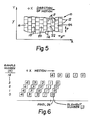
- the detector matrix 10 of the present invention is represented as a staggered array of square detector elements arranged in horizontal rows such as indicated at 12 and vertical columns such as indicated at 14. Each column 14 is vertically displaced or offset from adjacent columns by a distance equal to one half p, i.e., one half the side dimension of each square detector element.
- the modulation transfer function (MTF) is still given by the relation expressed in equations 2 and 3 above.
- the radiation-sensitive square faces of the detector elements are approximately 0.35 millimeters on a side.
- the staggered detector array includes 30 columns and 2016 rows having an overall dimension of approximately 10.5 by 352.8 millimeters.
- Each detector is of a known type, such as a photodiode coupled to an X-ray scintillator, which produces an analog charge signal in response to receipt of radiation incident on its sensitive surface. This charge is integrated during the time that the element's radiation sensitive face is exposed to the radiation.
- Time delay and integrate circuitry is coupled to , each row of detector elements. As the detector moves in the direction given by the arrow in Figure 5 relative to the patient, the TDI circuitry samples, delays and adds charge in a unique sequence, to enable great improvement in resolution in conjunction with the staggered array of detector elements. Each accumulation step is preceded by a sampling step.
- the Nyquist frequency is doubled in the y direction by staggering the detector elements.
- the Nyquist frequency is doubled in the x direction by sampling every detector half-width increment, in conjunction with use of the staggered array.
- the sampling takes place at a frequency such that a sampling occurs with each successive incremental relative movement of the detector by a distance of p/2. That is, the time delay and integrate circuitry samples the charge packets present at the detector element outputs along a row each time the detector array has moved a distance equal to half the length of a side of one of the square detector elements.
- a "row" of detector elements extending in the x direction as in Figure 5 is exemplified by the set of elements 16, 18; 20, 22, 24 as illustrated in that figure.
- the center-to-center spacing of elements in a given row extending in the x direction is 2p, or twice the lateral dimension of a side of a single one of the uniform detector elements.
- the sampling distance dictated by the staggered array geometry is p/2, because the rows are partially interspersed.
- the actual resolution obtainable in the y direction is now limited only by the aperture cutoff frequency, which, as described above, is twice as favorable as that dictated by the Nyquist spatial frequency which obtained in the prior art rectangular array system.
- the configuration of the present embodiment provides twice the resolution, in both directions, of that of the prior art.
- Pixel size in the present embodiment is only one quarter of the area of one detector element.
- the embodiment of this invention substantially reduces aliasing, compared to that of the standard prior art rectangular array.
- the staggered detector array requires associated time delay and integrate circuitry that differs from the circuitry whose operation is exemplified in equation 1.
- s(j,k) represent the k-th sample of the j-th element, where the elements are numbered from right to left and j ranges from 0 to 4 (see Figure 6).
- the image portion or pixel which is designated by the reference character 26 and which is aligned with element 0 at sample 0. Since the sampling distance in this embodiment is p/2, this particular pixel will be aligned with element 1 only at the fourth sampling, with element 2 at sample 8, element 3 at sample 12 and so on. Therefore, the final value generated by the time delay and integration circuitry and corresponding to this pixel will be:
- the shift and add sequence represented by equations 4 and 5 can be implemented in a variety of ways.
- a preferred implementation involves the use of CCD analog shift registers in a time delay integration configuration. It is important to note, however, that operating in this sequence, the TDI CCD cells cannot themselves constitute a portion of the detector elements. Rather, the detector elements must be separate from, but coupled to, the TDI circuitry.
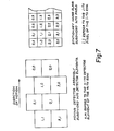
- Figure 8 illustrates the structure and operation of circuitry for implementing the time delay and integrate sequencing represented by equations 4 and 5.
- Figure 8 illustrates a portion of a detector array at eleven different steps of relative detector motion with respect to a patient, these steps being labeled from 0-10.
- step 0 two rows of detector elements are illustrated, there being two detector elements in each row, having their center-to-center spacing equal td 2p, where p is the dimension of one side of each of the square elements.
- td 2p the center-to-center spacing
- one row of such elements is designated 30, 32, while the other row is designated 34, 36.
- Detector element 32 is coupled by a lead 38 to a two-cell shift register 40.
- Detector element 30 is coupled by a lead 42 to a six element shift register 44.
- the outputs of the registers 40, 44 are connected in parallel to an output line 46.
- the output line 46 receives analog signals from the registers 40, 42 representing total charge value corresponding to a particular pixel or image portion which has been "read” by both of the detector elements 30, 32 in the detector element row of interest.
- Output lead 46 is coupled as an input to the ADC.
- the analog output of detector element 34 is coupled by a lead 50 to a four-cell shift register 52.
- the output of detector element 36 is coupled by a lead 54 directly in parallel with the output of the shift register 52, the resultant output being summed and appearing at an output lead 56.
- Analog signals appearing at the lead 56 are transmitted to the DPU for further processing in accordance with known techniques.
- Each output appearing at the lead 56 is an analog signal representing a total pixel value of an image portion which has been read by both the detector elements in the associated row, i.e., elements 34, 36.
- Each of the leads connected directly to elements 30, 32, 34, 36 comprises a translucent polysilicon conductor.
- signals at the leads 46, 56 are not mixed by the system, because they are signals representing different rows of data in the total image, elements 34, 36 representing an upper row and elements 30, 32 representing a lower row.
- a shaded band of radiation 60 is also illustrated in Figure 8.
- the radiation band 60 is to be considered as falling upon whatever detector element(s) are illustrated as within the band at any given step.
- radiation from the spread beam is continuously directed through a patient toward all of the detector elements simultaneously, the radiation falling upon individual detector elements in greater or lesser amounts depending on the patient's internal body structure.
- the radiation pattern emergent from the patient will be considered to be a slit having a width equal to that of the radiation band 60 illustrated in Figure 8.
- step 0 For purposes of clarity, the reference characters illustrated in conjunction with the illustration corresponding to step 0 are omitted for the other steps, in order to avoid undue cluttering of the drawing.
- the reference characters associated with the illustration of step 0 are to be considered as applicable also to the corresponding portions of the illustrations of the subsequent steps 1-10.
- the radiation band 60 is not incident on any portion of any of the detector elements. Therefore, none of the detector elements generate any charge packets constituting analog signals representing incident radiation.
- clocking circuitry of known type but not illustrated specifically in Figure 8, is provided. At each step increment, the clocking circuitry causes the signals at the leads 38, 42, 54 and 50 to be sampled. With respect to the leads 38, 42 and 50, which are coupled respectively to shift registers 40, 44, 52, the clocking circuitry causes a signal representing the respective charge packet from the associated element to be stored in the first cell of the corresponding shift register. The clocking signal also causes any previously stored charge related signals in each of the shift registers to shift to the next subsequent cell of that register. The clocking signal causes any signal stored in the ultimate cell of a shift register to proceed to the associated one of outputs 46, 56.
- the clocking circuitry executes its ensemble of operation as described above with a frequency such that the elements are sampled at successive increments of p/2 detector travel.
- the detector has moved to the right, relative to the patient, a distance of p/2, or half the width of a detector element.
- the detector element 30 is positioned such that half the detector element receives incident radiation from the slit radiation pattern 60.
- the element 30 generates a charge "packet" which is designated by a dot located in the center of that element.
- the other elements not being within the radiation slit 60, generate no charge packets.
- the.charge packet represented by the dot in the illustration of step 1 has been clocked into the first cell of the register 44.
- the element 30 is now completely illuminated with incident radiation from the slit pattern 60. Since the detector element generates charge packets in accordance with the amount of radiation received, this element produces an amount of charge at its output equal to two of the packets designated by the dot in step 1. This generated charge is represented by two dots within element 30 as illustrated in connection with step 2.
- step 3 Upon arrival at the location illustrated in connection with step 3, the double charge packet produced by element 30 is clocked into the first cell of the register 44.
- the single charge packet formerly located in the first cell of register 44 is clocked into the second cell of that register. Meanwhile, in a fashion analogous to that described above, both elements 30 and 34 generate single charge packets.
- step 6 This progression of generation and storage of charge packets continues. Note that it is not until step 6 that any charge from the element 32, in the same row as element 30, is clocked into the two-cell register 40. It will be recalled that charge, in this illustration, was first clocked into the register 44 at step 2, four steps previous to the first appearance of charge signal in the register 40. Thus, charge clocked into the register 44 is delayed by four p/2 increments of relative detector motion, with respect to charge in the register 40.
- equations 4 and 5 are implemented by providing each detector element in a row with a delay which is different and independent from the delay imposed on the outputs of other cells in the row.
- the prescribed delay sequences for implementing equations 4 and 5 can be built into the TDI circuitry coupled to the respective elements.
- Step 8 corresponds to an output representing two charge packets at the lead 46.
- the signal corresponding to two charge packets is derived from the summation of the two single charge representing signals present in the ultimate cells of each of the shift registers 44, 40.
- the clocking circuitry produces an output representing four charge packets, the result of the summation of the two signals each representing two charge packets present in the ultimate cells of the registers 44, 40 at step 8.
- a relative delay in output signals from the element 34, with respect to those from the element 36, is effected by the presence of the four-cell shift register 52 in the line 50, and by the fact that the output from the element 36 is presented directly over the lead 54 to the output 56.
- the signal-to-noise ratio of the output signals describing the respective image pixel is enhanced. If the TDI circuitry illustrated in Figure.8 were not used, the output of, for example, element 30, in passing through the radiation slit 60 would be a succession of three 0176314 signals representing 1, 2 and 1 charge packet, respectively, which would be emitted at steps 1, 2 and 3.
- the corresponding outputs are signals representing 2, 4 and 2 charge packets, occuring at steps 8, 9 and 10.
- Figure 8 constitutes an illustration of the operation and components of the TDI circuitry in a simplified environment, i.e., considering only two rows of two detector elements each. Those of skill in the art will easily be able to expand this illustration in an analogous fashion to the use of larger numbers of elements in each row, and to larger numbers of rows. For example, if three elements were employed in each row, the right hand element in Figure 8 would have its output coupled to a ten-cell shift register. The middle element will be coupled to a six-cell register and the left hand, or third element would be coupled to a two-cell register. This configuration would maintain the respective delay relationships in summing signals from the respective elements as expressed in equations 4 and 5 above.
Landscapes
- Health & Medical Sciences (AREA)
- Life Sciences & Earth Sciences (AREA)
- Engineering & Computer Science (AREA)
- Medical Informatics (AREA)
- Physics & Mathematics (AREA)
- Molecular Biology (AREA)
- Biomedical Technology (AREA)
- General Health & Medical Sciences (AREA)
- Nuclear Medicine, Radiotherapy & Molecular Imaging (AREA)
- Optics & Photonics (AREA)
- High Energy & Nuclear Physics (AREA)
- Spectroscopy & Molecular Physics (AREA)
- General Physics & Mathematics (AREA)
- Biophysics (AREA)
- Pathology (AREA)
- Radiology & Medical Imaging (AREA)
- Heart & Thoracic Surgery (AREA)
- Surgery (AREA)
- Animal Behavior & Ethology (AREA)
- Public Health (AREA)
- Veterinary Medicine (AREA)
- Apparatus For Radiation Diagnosis (AREA)
- Analysing Materials By The Use Of Radiation (AREA)
- Transforming Light Signals Into Electric Signals (AREA)
Applications Claiming Priority (2)
| Application Number | Priority Date | Filing Date | Title |
|---|---|---|---|
| US65395584A | 1984-09-21 | 1984-09-21 | |
| US653955 | 1984-09-21 |
Publications (3)
| Publication Number | Publication Date |
|---|---|
| EP0176314A2 true EP0176314A2 (de) | 1986-04-02 |
| EP0176314A3 EP0176314A3 (en) | 1987-06-16 |
| EP0176314B1 EP0176314B1 (de) | 1992-06-10 |
Family
ID=24622947
Family Applications (1)
| Application Number | Title | Priority Date | Filing Date |
|---|---|---|---|
| EP19850306633 Expired EP0176314B1 (de) | 1984-09-21 | 1985-09-18 | Röntgen-Anordnung |
Country Status (4)
| Country | Link |
|---|---|
| EP (1) | EP0176314B1 (de) |
| JP (1) | JPH0661324B2 (de) |
| CA (1) | CA1240074A (de) |
| DE (1) | DE3586192T2 (de) |
Cited By (16)
| Publication number | Priority date | Publication date | Assignee | Title |
|---|---|---|---|---|
| FR2668829A1 (fr) * | 1990-11-05 | 1992-05-07 | Commissariat Energie Atomique | Dispositif et procede de controle non destructif a acquisition simultanee de donnees radiographiques et de donnees tomographiques. |
| WO1997040737A2 (en) * | 1996-04-29 | 1997-11-06 | Osteometer Meditech A/S | X-ray apparatus |
| FR2767261A1 (fr) * | 1997-08-01 | 1999-02-19 | Sirona Dental Systems Gmbh | Dispositif de diagnostic aux rayons x pour l'elaboration de tomographies panoramiques de parties du corps d'un patient |
| US9625606B2 (en) | 2009-05-16 | 2017-04-18 | Rapiscan Systems, Inc. | Systems and methods for high-Z threat alarm resolution |
| US9632205B2 (en) | 2011-02-08 | 2017-04-25 | Rapiscan Systems, Inc. | Covert surveillance using multi-modality sensing |
| US9688517B2 (en) | 2008-05-20 | 2017-06-27 | Rapiscan Systems, Inc. | Scanner systems |
| US9791590B2 (en) | 2013-01-31 | 2017-10-17 | Rapiscan Systems, Inc. | Portable security inspection system |
| US9817151B2 (en) | 2008-02-28 | 2017-11-14 | Rapiscan Systems, Inc. | Drive-through scanning systems |
| US9835756B2 (en) | 2008-02-28 | 2017-12-05 | Rapiscan Systems, Inc. | Dual mode X-ray vehicle scanning system |
| US10007021B2 (en) | 2008-02-28 | 2018-06-26 | Rapiscan Systems, Inc. | Scanning systems |
| US10007019B2 (en) | 2002-07-23 | 2018-06-26 | Rapiscan Systems, Inc. | Compact mobile cargo scanning system |
| US10098214B2 (en) | 2008-05-20 | 2018-10-09 | Rapiscan Systems, Inc. | Detector support structures for gantry scanner systems |
| US10585207B2 (en) | 2008-02-28 | 2020-03-10 | Rapiscan Systems, Inc. | Scanning systems |
| WO2022003141A1 (de) * | 2020-07-02 | 2022-01-06 | Smiths Detection Germany Gmbh | Dual-energie-detektor und aufbereitungsverfahren für detektordaten |
| US11796489B2 (en) | 2021-02-23 | 2023-10-24 | Rapiscan Systems, Inc. | Systems and methods for eliminating cross-talk signals in one or more scanning systems having multiple X-ray sources |
| US12061309B2 (en) | 2008-02-28 | 2024-08-13 | Rapiscan Systems, Inc. | Drive-through scanning systems |
Families Citing this family (15)
| Publication number | Priority date | Publication date | Assignee | Title |
|---|---|---|---|---|
| US4873708A (en) * | 1987-05-11 | 1989-10-10 | General Electric Company | Digital radiographic imaging system and method therefor |
| FI119173B (fi) * | 2001-11-23 | 2008-08-29 | Planmed Oy | Anturijärjestely ja menetelmä digitaalisessa pyyhkäisykuvantamisessa |
| US7963695B2 (en) | 2002-07-23 | 2011-06-21 | Rapiscan Systems, Inc. | Rotatable boom cargo scanning system |
| US6928141B2 (en) | 2003-06-20 | 2005-08-09 | Rapiscan, Inc. | Relocatable X-ray imaging system and method for inspecting commercial vehicles and cargo containers |
| ATE422333T1 (de) * | 2004-01-29 | 2009-02-15 | Koninkl Philips Electronics Nv | Computertomographie-darstellung mit pixel-versatz und fokaler punkt-modulation |
| US7471764B2 (en) | 2005-04-15 | 2008-12-30 | Rapiscan Security Products, Inc. | X-ray imaging system having improved weather resistance |
| US7526064B2 (en) | 2006-05-05 | 2009-04-28 | Rapiscan Security Products, Inc. | Multiple pass cargo inspection system |
| GB0803643D0 (en) | 2008-02-28 | 2008-04-02 | Rapiscan Security Products Inc | Mobile scanning systems |
| GB0803641D0 (en) | 2008-02-28 | 2008-04-02 | Rapiscan Security Products Inc | Scanning systems |
| GB0809107D0 (en) | 2008-05-20 | 2008-06-25 | Rapiscan Security Products Inc | Scannign systems |
| US8963094B2 (en) | 2008-06-11 | 2015-02-24 | Rapiscan Systems, Inc. | Composite gamma-neutron detection system |
| GB0810638D0 (en) | 2008-06-11 | 2008-07-16 | Rapiscan Security Products Inc | Photomultiplier and detection systems |
| US9218933B2 (en) | 2011-06-09 | 2015-12-22 | Rapidscan Systems, Inc. | Low-dose radiographic imaging system |
| JP5831440B2 (ja) | 2012-12-17 | 2015-12-09 | 株式会社ダイヤメット | 粉末冶金用原料粉末 |
| US9557427B2 (en) | 2014-01-08 | 2017-01-31 | Rapiscan Systems, Inc. | Thin gap chamber neutron detectors |
Citations (4)
| Publication number | Priority date | Publication date | Assignee | Title |
|---|---|---|---|---|
| US3717762A (en) * | 1970-09-21 | 1973-02-20 | Baird Atomic Inc | Sensing matrix for a radioactivity-distribution detector |
| US4176280A (en) * | 1977-04-19 | 1979-11-27 | Siemens Aktiengesellschaft | Tomographic x-ray apparatus for producing transverse layer images |
| US4383327A (en) * | 1980-12-01 | 1983-05-10 | University Of Utah | Radiographic systems employing multi-linear arrays of electronic radiation detectors |
| FR2549711A1 (fr) * | 1983-07-28 | 1985-02-01 | Elscint Ltd | Appareil de tomographie informatisee et son procede de commande |
Family Cites Families (3)
| Publication number | Priority date | Publication date | Assignee | Title |
|---|---|---|---|---|
| JPS5784040A (en) * | 1980-11-13 | 1982-05-26 | Hitachi Medical Corp | X-ray photographing apparatus |
| JPS57195444A (en) * | 1981-05-26 | 1982-12-01 | Tokyo Shibaura Electric Co | X-ray photographing apparatus |
| EP0089148B1 (de) * | 1982-03-15 | 1987-02-25 | The Board Of Trustees Of The Leland Stanford Junior University | Detektorenmatrix zur Verwendung in der Radiographie |
-
1985
- 1985-09-18 DE DE19853586192 patent/DE3586192T2/de not_active Expired - Fee Related
- 1985-09-18 EP EP19850306633 patent/EP0176314B1/de not_active Expired
- 1985-09-20 JP JP60208582A patent/JPH0661324B2/ja not_active Expired - Lifetime
- 1985-09-20 CA CA000491174A patent/CA1240074A/en not_active Expired
Patent Citations (4)
| Publication number | Priority date | Publication date | Assignee | Title |
|---|---|---|---|---|
| US3717762A (en) * | 1970-09-21 | 1973-02-20 | Baird Atomic Inc | Sensing matrix for a radioactivity-distribution detector |
| US4176280A (en) * | 1977-04-19 | 1979-11-27 | Siemens Aktiengesellschaft | Tomographic x-ray apparatus for producing transverse layer images |
| US4383327A (en) * | 1980-12-01 | 1983-05-10 | University Of Utah | Radiographic systems employing multi-linear arrays of electronic radiation detectors |
| FR2549711A1 (fr) * | 1983-07-28 | 1985-02-01 | Elscint Ltd | Appareil de tomographie informatisee et son procede de commande |
Cited By (31)
| Publication number | Priority date | Publication date | Assignee | Title |
|---|---|---|---|---|
| EP0485265A1 (de) * | 1990-11-05 | 1992-05-13 | Commissariat A L'energie Atomique | Verfahren und Methode zur zerstörungsfreien Prüfung mit gleichzeitiger Aufnahme von Röntgendaten und tomographischen Daten |
| US5164971A (en) * | 1990-11-05 | 1992-11-17 | Commissariat A L'energie Atomique | Non-destructive testing apparatus and process with simultaneous acquisition of radiographic data and tomographic data |
| FR2668829A1 (fr) * | 1990-11-05 | 1992-05-07 | Commissariat Energie Atomique | Dispositif et procede de controle non destructif a acquisition simultanee de donnees radiographiques et de donnees tomographiques. |
| WO1997040737A2 (en) * | 1996-04-29 | 1997-11-06 | Osteometer Meditech A/S | X-ray apparatus |
| WO1997040737A3 (en) * | 1996-04-29 | 1998-04-09 | Osteometer Meditech As | X-ray apparatus |
| FR2767261A1 (fr) * | 1997-08-01 | 1999-02-19 | Sirona Dental Systems Gmbh | Dispositif de diagnostic aux rayons x pour l'elaboration de tomographies panoramiques de parties du corps d'un patient |
| US10007019B2 (en) | 2002-07-23 | 2018-06-26 | Rapiscan Systems, Inc. | Compact mobile cargo scanning system |
| US10670769B2 (en) | 2002-07-23 | 2020-06-02 | Rapiscan Systems, Inc. | Compact mobile cargo scanning system |
| US9817151B2 (en) | 2008-02-28 | 2017-11-14 | Rapiscan Systems, Inc. | Drive-through scanning systems |
| US12061309B2 (en) | 2008-02-28 | 2024-08-13 | Rapiscan Systems, Inc. | Drive-through scanning systems |
| US11275194B2 (en) | 2008-02-28 | 2022-03-15 | Rapiscan Systems, Inc. | Scanning systems |
| US9835756B2 (en) | 2008-02-28 | 2017-12-05 | Rapiscan Systems, Inc. | Dual mode X-ray vehicle scanning system |
| US10007021B2 (en) | 2008-02-28 | 2018-06-26 | Rapiscan Systems, Inc. | Scanning systems |
| US11768313B2 (en) | 2008-02-28 | 2023-09-26 | Rapiscan Systems, Inc. | Multi-scanner networked systems for performing material discrimination processes on scanned objects |
| US11579328B2 (en) | 2008-02-28 | 2023-02-14 | Rapiscan Systems, Inc. | Drive-through scanning systems |
| US10585207B2 (en) | 2008-02-28 | 2020-03-10 | Rapiscan Systems, Inc. | Scanning systems |
| US10754058B2 (en) | 2008-02-28 | 2020-08-25 | Rapiscan Systems, Inc. | Drive-through scanning systems |
| US10816691B2 (en) | 2008-02-28 | 2020-10-27 | Rapiscan Systems, Inc. | Multi-element detector systems |
| US9688517B2 (en) | 2008-05-20 | 2017-06-27 | Rapiscan Systems, Inc. | Scanner systems |
| US10098214B2 (en) | 2008-05-20 | 2018-10-09 | Rapiscan Systems, Inc. | Detector support structures for gantry scanner systems |
| US9625606B2 (en) | 2009-05-16 | 2017-04-18 | Rapiscan Systems, Inc. | Systems and methods for high-Z threat alarm resolution |
| US9632205B2 (en) | 2011-02-08 | 2017-04-25 | Rapiscan Systems, Inc. | Covert surveillance using multi-modality sensing |
| US10942291B2 (en) | 2011-02-08 | 2021-03-09 | Rapiscan Systems, Inc. | Covert surveillance using multi-modality sensing |
| US11307325B2 (en) | 2011-02-08 | 2022-04-19 | Rapiscan Systems, Inc. | Covert surveillance using multi-modality sensing |
| US10408967B2 (en) | 2011-02-08 | 2019-09-10 | Rapiscan Systems, Inc. | Covert surveillance using multi-modality sensing |
| US11822041B2 (en) | 2011-02-08 | 2023-11-21 | Rapiscan Systems, Inc. | Systems and methods for improved atomic-number based material discrimination |
| US11550077B2 (en) | 2013-01-31 | 2023-01-10 | Rapiscan Systems, Inc. | Portable vehicle inspection portal with accompanying workstation |
| US10317566B2 (en) | 2013-01-31 | 2019-06-11 | Rapiscan Systems, Inc. | Portable security inspection system |
| US9791590B2 (en) | 2013-01-31 | 2017-10-17 | Rapiscan Systems, Inc. | Portable security inspection system |
| WO2022003141A1 (de) * | 2020-07-02 | 2022-01-06 | Smiths Detection Germany Gmbh | Dual-energie-detektor und aufbereitungsverfahren für detektordaten |
| US11796489B2 (en) | 2021-02-23 | 2023-10-24 | Rapiscan Systems, Inc. | Systems and methods for eliminating cross-talk signals in one or more scanning systems having multiple X-ray sources |
Also Published As
| Publication number | Publication date |
|---|---|
| EP0176314A3 (en) | 1987-06-16 |
| JPS61122847A (ja) | 1986-06-10 |
| DE3586192T2 (de) | 1993-01-14 |
| JPH0661324B2 (ja) | 1994-08-17 |
| CA1240074A (en) | 1988-08-02 |
| EP0176314B1 (de) | 1992-06-10 |
| DE3586192D1 (de) | 1992-07-16 |
Similar Documents
| Publication | Publication Date | Title |
|---|---|---|
| US4817123A (en) | Digital radiography detector resolution improvement | |
| EP0176314B1 (de) | Röntgen-Anordnung | |
| US4383327A (en) | Radiographic systems employing multi-linear arrays of electronic radiation detectors | |
| EP0182529B1 (de) | Röntgenanlage | |
| US4477922A (en) | Tomographic x-ray apparatus for the production of transverse layer images | |
| US4196352A (en) | Multiple purpose high speed tomographic x-ray scanner | |
| US6760404B2 (en) | Radiation detector and X-ray CT apparatus | |
| CA1282192C (en) | Method and apparatus for utilizing an electro-optic detector in a microtomography system | |
| US6359279B1 (en) | Detector for nuclear imaging | |
| USRE37536E1 (en) | Split energy level radiation detection | |
| EP0051350B1 (de) | Abtastblende zur Darstellung einer Absorptionsverteilung mittels eines Sichtgerätes | |
| US4389729A (en) | High resolution digital radiography system | |
| GB1585364A (en) | Device for measuring the absorption of radiation in a body section | |
| EP0061496A4 (de) | Detektor-system mit bildverstärker für elektronische röntgenaufnahmen. | |
| EP0166567A2 (de) | Vorrichtung und Verfahren zur Bilderzeugung | |
| JPS6298284A (ja) | 陽電子放射断層放射線カメラ | |
| EP0089148A1 (de) | Detektorenmatrix zur Verwendung in der Radiographie | |
| CN1135430C (zh) | 计算机层析x射线摄影机 | |
| JP2606207B2 (ja) | 画像撮影装置 | |
| GB1602521A (en) | Arrangement for producing an image of a body section using gamma or x-radiation | |
| US5867554A (en) | Spiral scan computed tomography apparatus having a modular surface detector for radiation | |
| USRE32164E (en) | Radiographic systems employing multi-linear arrays of electronic radiation detectors | |
| US4066900A (en) | Technique for cat utilizing composite beam paths which are wider at their ends than therebetween | |
| US4481650A (en) | Installation for producing radiographic layer images | |
| USRE32779E (en) | Radiographic systems employing multi-linear arrays of electronic radiation detectors |
Legal Events
| Date | Code | Title | Description |
|---|---|---|---|
| PUAI | Public reference made under article 153(3) epc to a published international application that has entered the european phase |
Free format text: ORIGINAL CODE: 0009012 |
|
| AK | Designated contracting states |
Kind code of ref document: A2 Designated state(s): DE FR GB NL |
|
| PUAL | Search report despatched |
Free format text: ORIGINAL CODE: 0009013 |
|
| AK | Designated contracting states |
Kind code of ref document: A3 Designated state(s): DE FR GB NL |
|
| 17P | Request for examination filed |
Effective date: 19871029 |
|
| 17Q | First examination report despatched |
Effective date: 19900903 |
|
| GRAA | (expected) grant |
Free format text: ORIGINAL CODE: 0009210 |
|
| AK | Designated contracting states |
Kind code of ref document: B1 Designated state(s): DE FR GB NL |
|
| ET | Fr: translation filed | ||
| REF | Corresponds to: |
Ref document number: 3586192 Country of ref document: DE Date of ref document: 19920716 |
|
| PLBE | No opposition filed within time limit |
Free format text: ORIGINAL CODE: 0009261 |
|
| STAA | Information on the status of an ep patent application or granted ep patent |
Free format text: STATUS: NO OPPOSITION FILED WITHIN TIME LIMIT |
|
| 26N | No opposition filed | ||
| PGFP | Annual fee paid to national office [announced via postgrant information from national office to epo] |
Ref country code: GB Payment date: 19980825 Year of fee payment: 14 |
|
| PGFP | Annual fee paid to national office [announced via postgrant information from national office to epo] |
Ref country code: FR Payment date: 19980909 Year of fee payment: 14 |
|
| PGFP | Annual fee paid to national office [announced via postgrant information from national office to epo] |
Ref country code: DE Payment date: 19980925 Year of fee payment: 14 |
|
| PGFP | Annual fee paid to national office [announced via postgrant information from national office to epo] |
Ref country code: NL Payment date: 19980929 Year of fee payment: 14 |
|
| PG25 | Lapsed in a contracting state [announced via postgrant information from national office to epo] |
Ref country code: GB Free format text: LAPSE BECAUSE OF NON-PAYMENT OF DUE FEES Effective date: 19990918 |
|
| PG25 | Lapsed in a contracting state [announced via postgrant information from national office to epo] |
Ref country code: NL Free format text: LAPSE BECAUSE OF NON-PAYMENT OF DUE FEES Effective date: 20000401 |
|
| GBPC | Gb: european patent ceased through non-payment of renewal fee |
Effective date: 19990918 |
|
| PG25 | Lapsed in a contracting state [announced via postgrant information from national office to epo] |
Ref country code: FR Free format text: LAPSE BECAUSE OF NON-PAYMENT OF DUE FEES Effective date: 20000531 |
|
| NLV4 | Nl: lapsed or anulled due to non-payment of the annual fee |
Effective date: 20000401 |
|
| PG25 | Lapsed in a contracting state [announced via postgrant information from national office to epo] |
Ref country code: DE Free format text: LAPSE BECAUSE OF NON-PAYMENT OF DUE FEES Effective date: 20000701 |
|
| REG | Reference to a national code |
Ref country code: FR Ref legal event code: ST |