EP0176030A2 - Ultrasonic transducer and method of manufacturing same - Google Patents
Ultrasonic transducer and method of manufacturing same Download PDFInfo
- Publication number
- EP0176030A2 EP0176030A2 EP85111818A EP85111818A EP0176030A2 EP 0176030 A2 EP0176030 A2 EP 0176030A2 EP 85111818 A EP85111818 A EP 85111818A EP 85111818 A EP85111818 A EP 85111818A EP 0176030 A2 EP0176030 A2 EP 0176030A2
- Authority
- EP
- European Patent Office
- Prior art keywords
- electrode
- flexible substrate
- piezoelectric member
- electrodes
- lead conductor
- Prior art date
- Legal status (The legal status is an assumption and is not a legal conclusion. Google has not performed a legal analysis and makes no representation as to the accuracy of the status listed.)
- Granted
Links
- 238000004519 manufacturing process Methods 0.000 title claims abstract description 39
- 239000000758 substrate Substances 0.000 claims abstract description 135
- 239000002861 polymer material Substances 0.000 claims abstract description 21
- 239000004020 conductor Substances 0.000 claims description 90
- 239000000853 adhesive Substances 0.000 claims description 65
- 230000001070 adhesive effect Effects 0.000 claims description 65
- 229920000642 polymer Polymers 0.000 claims description 26
- 238000000034 method Methods 0.000 claims description 23
- 239000002131 composite material Substances 0.000 claims description 17
- 230000007261 regionalization Effects 0.000 claims description 8
- 238000003825 pressing Methods 0.000 claims description 7
- 230000015572 biosynthetic process Effects 0.000 claims description 5
- 238000000151 deposition Methods 0.000 claims description 4
- 229920001577 copolymer Polymers 0.000 description 14
- 239000000523 sample Substances 0.000 description 14
- 239000000463 material Substances 0.000 description 7
- 230000035945 sensitivity Effects 0.000 description 6
- 239000002033 PVDF binder Substances 0.000 description 5
- 239000011159 matrix material Substances 0.000 description 5
- 229920002981 polyvinylidene fluoride Polymers 0.000 description 5
- FCYVWWWTHPPJII-UHFFFAOYSA-N 2-methylidenepropanedinitrile Chemical compound N#CC(=C)C#N FCYVWWWTHPPJII-UHFFFAOYSA-N 0.000 description 4
- RYGMFSIKBFXOCR-UHFFFAOYSA-N Copper Chemical compound [Cu] RYGMFSIKBFXOCR-UHFFFAOYSA-N 0.000 description 4
- 230000010287 polarization Effects 0.000 description 4
- 238000003491 array Methods 0.000 description 3
- 239000011889 copper foil Substances 0.000 description 3
- 238000003325 tomography Methods 0.000 description 3
- 238000007740 vapor deposition Methods 0.000 description 3
- 230000015556 catabolic process Effects 0.000 description 2
- 239000000919 ceramic Substances 0.000 description 2
- 239000011248 coating agent Substances 0.000 description 2
- 238000000576 coating method Methods 0.000 description 2
- 230000005684 electric field Effects 0.000 description 2
- 239000011888 foil Substances 0.000 description 2
- 238000009413 insulation Methods 0.000 description 2
- 239000012212 insulator Substances 0.000 description 2
- 230000004048 modification Effects 0.000 description 2
- 238000012986 modification Methods 0.000 description 2
- 229920002239 polyacrylonitrile Polymers 0.000 description 2
- 229920002620 polyvinyl fluoride Polymers 0.000 description 2
- 229910000679 solder Inorganic materials 0.000 description 2
- XFXPMWWXUTWYJX-UHFFFAOYSA-N Cyanide Chemical compound N#[C-] XFXPMWWXUTWYJX-UHFFFAOYSA-N 0.000 description 1
- 239000004677 Nylon Substances 0.000 description 1
- 229930182556 Polyacetal Natural products 0.000 description 1
- 239000004642 Polyimide Substances 0.000 description 1
- 239000002253 acid Substances 0.000 description 1
- 230000002411 adverse Effects 0.000 description 1
- XAGFODPZIPBFFR-UHFFFAOYSA-N aluminium Chemical compound [Al] XAGFODPZIPBFFR-UHFFFAOYSA-N 0.000 description 1
- 229910052782 aluminium Inorganic materials 0.000 description 1
- 230000003466 anti-cipated effect Effects 0.000 description 1
- 230000005540 biological transmission Effects 0.000 description 1
- OTHBGZRSQZUQAH-UHFFFAOYSA-N chloroethene 2-methylidenepropanedinitrile Chemical compound C(=C)Cl.C(=C)(C#N)C#N OTHBGZRSQZUQAH-UHFFFAOYSA-N 0.000 description 1
- 230000000052 comparative effect Effects 0.000 description 1
- 229910052802 copper Inorganic materials 0.000 description 1
- 239000010949 copper Substances 0.000 description 1
- 238000005520 cutting process Methods 0.000 description 1
- 238000003745 diagnosis Methods 0.000 description 1
- 230000003292 diminished effect Effects 0.000 description 1
- 230000000694 effects Effects 0.000 description 1
- 238000010438 heat treatment Methods 0.000 description 1
- 239000011810 insulating material Substances 0.000 description 1
- 238000004898 kneading Methods 0.000 description 1
- HFGPZNIAWCZYJU-UHFFFAOYSA-N lead zirconate titanate Chemical compound [O-2].[O-2].[O-2].[O-2].[O-2].[Ti+4].[Zr+4].[Pb+2] HFGPZNIAWCZYJU-UHFFFAOYSA-N 0.000 description 1
- 229910052451 lead zirconate titanate Inorganic materials 0.000 description 1
- WABPQHHGFIMREM-UHFFFAOYSA-N lead(0) Chemical compound [Pb] WABPQHHGFIMREM-UHFFFAOYSA-N 0.000 description 1
- 238000009659 non-destructive testing Methods 0.000 description 1
- 229920001778 nylon Polymers 0.000 description 1
- 230000010355 oscillation Effects 0.000 description 1
- 238000001259 photo etching Methods 0.000 description 1
- 229920000728 polyester Polymers 0.000 description 1
- 229920001721 polyimide Polymers 0.000 description 1
- 229920006324 polyoxymethylene Polymers 0.000 description 1
- 229920000915 polyvinyl chloride Polymers 0.000 description 1
- 239000004800 polyvinyl chloride Substances 0.000 description 1
- 229920000131 polyvinylidene Polymers 0.000 description 1
- 239000000843 powder Substances 0.000 description 1
- 230000003014 reinforcing effect Effects 0.000 description 1
- 229920005989 resin Polymers 0.000 description 1
- 239000011347 resin Substances 0.000 description 1
- 229910052709 silver Inorganic materials 0.000 description 1
- 239000004332 silver Substances 0.000 description 1
- 238000005476 soldering Methods 0.000 description 1
- 230000002269 spontaneous effect Effects 0.000 description 1
- 239000013589 supplement Substances 0.000 description 1
- 229920002554 vinyl polymer Polymers 0.000 description 1
Images


Classifications
-
- B—PERFORMING OPERATIONS; TRANSPORTING
- B06—GENERATING OR TRANSMITTING MECHANICAL VIBRATIONS IN GENERAL
- B06B—METHODS OR APPARATUS FOR GENERATING OR TRANSMITTING MECHANICAL VIBRATIONS OF INFRASONIC, SONIC, OR ULTRASONIC FREQUENCY, e.g. FOR PERFORMING MECHANICAL WORK IN GENERAL
- B06B1/00—Methods or apparatus for generating mechanical vibrations of infrasonic, sonic, or ultrasonic frequency
- B06B1/02—Methods or apparatus for generating mechanical vibrations of infrasonic, sonic, or ultrasonic frequency making use of electrical energy
- B06B1/06—Methods or apparatus for generating mechanical vibrations of infrasonic, sonic, or ultrasonic frequency making use of electrical energy operating with piezoelectric effect or with electrostriction
- B06B1/0688—Methods or apparatus for generating mechanical vibrations of infrasonic, sonic, or ultrasonic frequency making use of electrical energy operating with piezoelectric effect or with electrostriction with foil-type piezoelectric elements, e.g. PVDF
-
- Y—GENERAL TAGGING OF NEW TECHNOLOGICAL DEVELOPMENTS; GENERAL TAGGING OF CROSS-SECTIONAL TECHNOLOGIES SPANNING OVER SEVERAL SECTIONS OF THE IPC; TECHNICAL SUBJECTS COVERED BY FORMER USPC CROSS-REFERENCE ART COLLECTIONS [XRACs] AND DIGESTS
- Y10—TECHNICAL SUBJECTS COVERED BY FORMER USPC
- Y10S—TECHNICAL SUBJECTS COVERED BY FORMER USPC CROSS-REFERENCE ART COLLECTIONS [XRACs] AND DIGESTS
- Y10S310/00—Electrical generator or motor structure
- Y10S310/80—Piezoelectric polymers, e.g. PVDF
-
- Y—GENERAL TAGGING OF NEW TECHNOLOGICAL DEVELOPMENTS; GENERAL TAGGING OF CROSS-SECTIONAL TECHNOLOGIES SPANNING OVER SEVERAL SECTIONS OF THE IPC; TECHNICAL SUBJECTS COVERED BY FORMER USPC CROSS-REFERENCE ART COLLECTIONS [XRACs] AND DIGESTS
- Y10—TECHNICAL SUBJECTS COVERED BY FORMER USPC
- Y10T—TECHNICAL SUBJECTS COVERED BY FORMER US CLASSIFICATION
- Y10T29/00—Metal working
- Y10T29/42—Piezoelectric device making
-
- Y—GENERAL TAGGING OF NEW TECHNOLOGICAL DEVELOPMENTS; GENERAL TAGGING OF CROSS-SECTIONAL TECHNOLOGIES SPANNING OVER SEVERAL SECTIONS OF THE IPC; TECHNICAL SUBJECTS COVERED BY FORMER USPC CROSS-REFERENCE ART COLLECTIONS [XRACs] AND DIGESTS
- Y10—TECHNICAL SUBJECTS COVERED BY FORMER USPC
- Y10T—TECHNICAL SUBJECTS COVERED BY FORMER US CLASSIFICATION
- Y10T29/00—Metal working
- Y10T29/49—Method of mechanical manufacture
- Y10T29/49002—Electrical device making
- Y10T29/49117—Conductor or circuit manufacturing
- Y10T29/49124—On flat or curved insulated base, e.g., printed circuit, etc.
- Y10T29/4913—Assembling to base an electrical component, e.g., capacitor, etc.
- Y10T29/49144—Assembling to base an electrical component, e.g., capacitor, etc. by metal fusion
Definitions
- This invention relates to an ultrasonic transducer and to a method of manufacturing the same.
- Ultrasonic transducers are widely employed as the probes in ultrasonic diagnostic equipment for real-time . tomography, in ultrasonic materials testing equipment for the non-destructive testing of materials, and in many other applications.
- An ultrasonic transducer generally is of a structure that includes a vibrator comprising a piezoelectric element for generating ultrasonic waves conforming to a driving voltage or for converting a received ultrasonic wave into an electric signal, an acoustic matching layer for acoustic impedence matching with a specimen under examination, and a backing member for absorbing both free oscillation of the vibrator and ultrasonic waves that emerge from the back surface, the vibrator, acoustic matching layer and backing being disposed in laminated relation.
- a film-like piezoelectric polymer member formed from a piezoelectric polymer such as a polyvinylidene fluoride (PVDF) resin.
- PVDF polyvinylidene fluoride
- a piezoelectric polymer member such as of PVDF exhibits excellent acoustic matching with respect to a living body since its acoustic impedence is closer to that of a living body than is the acoustic impedence of conventional ceramic piezoelectric members.
- Such a piezoelectric member also has a low mechanical Q, as a result of which improved sensitivity and response are anticipated, and exhibits flexibility that enables the vibrator to be machined into almost any shape with comparative ease.
- the piezoelectric member generally is embraced by a pair of electrodes necessary for applying a driving voltage to the piezoelectric member or for detecting a received signal in the form of a voltage, and each electrode must be provided with a lead wire for connecting the electrode to a separately provided transmitter circuit, which supplies the abovementioned driving voltage, or to a separate receiver circuit that receives a signal from the piezoelectric member.
- a first object of the present invention is to provide an ultrasonic transducer having excellent acoustic characteristics, sensitivity and response and capable of being manufactured through a shorter manufacturing process without subjecting a piezoelectric polymer member to the effects of heat.
- a second object of the present invention is to provide a method of manufacturing such an ultrasonic transducer.
- An ultrasonic transducer comprises a piezoelectric member formed from a piezoelectric polymer material or a piezoelectric polymer composite and having a pair of main surfaces, a first electrode bonded to one of the main surfaces of the piezoelectric member by an adhesive bond so as to substantially cover the one main surface, a second electrode bonded to the other of the main surfaces of the piezoelectric member by an adhesive bond so as to substantially cover the other main surface, a first lead conductor connected to the first electrode for leading the first electrode out to an external terminal, and a second lead conductor connected to the second electrode for leading the second electrode out to an external terminal.
- the first electrode and the first lead conductor are formed integral with a first flexible substrate, and the second electrode and the second lead conductor are formed integral with the first flexible substrate or with a second flexible substrate.
- the piezoelectric member is polarized at least by applying a voltage across the first and second electrodes.
- the ultrasonic transducer comprises a piezoelectric member formed from a piezoelectric polymer material or a piezoelectric polymer composite and having a pair of main surfaces, a first electrode bonded to one of the main surfaces of the piezoelectric member by an adhesive bond so as to substantially cover the one main surface, a second electrode deposited on the other of the main surfaces of the piezoelectric member so as to substantially cover the other main surface, a first lead conductor connected to the first electrode for leading the first electrode out to an external terminal, and a second lead conductor having an electrode contact portion contacting an edge portion of the second electrode for leading the second electrode out to an external terminal.
- the first electrode and the first lead conductor are formed integral with a flexible first substrate, the second lead conductor is formed on the first flexible substrate or on a flexible second substrate, the electrode contact portion is brought into intimate pressing contact with the second electrode by bonding the substrate with which the second lead conductor is formed to the second electrode via an adhesive bond, and the piezoelectric member is polarized at least by applying a voltage across the first and second electrodes.
- the first electrode comprises a plurality of electrodes arranged in a side-by-side array
- the second electrode comprises a single electrode arranged to commonly oppose the first electrode.
- the first and second electrodes each comprise a plurality of electrodes arranged in a side-by-side array, and the first and second electrodes are arranged to oppose each other in such a manner that the array of the first electrode is oriented perpendicular to the array of the second electrode.
- the first or second electrode comprises a plurality of electrodes
- the adhesive bond between the electrodes and the piezoelectric member comprises an adhesive possessing anisotropic electrical conductivity
- the flexible substrate on which the second electrode is formed may be provided with an acoustic matching layer.
- a method of manufacturing an ultrasonic transducer comprises a conductive pattern formation step of forming a first electrode and a first lead conductor integral with a flexible first substrate on a surface thereof, the first lead conductor extending along the surface of the first substrate starting from a side edge of the first electrode, and forming a second electrode and a second lead conductor integral with the flexible first substrate or a flexible second substrate on a surface thereof, the second lead conductor extending along the surface of the substrate starting from a side edge of the second electrode, a bonding step of bonding the first and second electrodes to opposing first and second main surfaces of a piezoelectric member, which is formed from a piezoelectric polymer material or a piezoelectric polymer composite, by applying an adhesive to a surface of the first electrode and to a surface of the second electrode, and a polarizing step of polarizing the piezoelectric member at least by applying a voltage across the first and second electrodes.
- Another embodiment of a method of manufacturing an ultrasonic transducer comprises a conductive pattern formation step of forming a first electrode and a first lead conductor integral with a flexible first substrate on a surface thereof, the first lead conductor extending along the surface of the first substrate starting from a side edge of the first electrode, and forming a second lead conductor having an electrode contact portion at one end thereof on the flexible first substrate or a flexible second substrate, a second electrode formation step of depositing a second electrode on a first main surface of a piezoelectric member formed from a piezoelectric polymer material or a piezoelectric polymer composite, a bonding step of bonding the first electrode to a second main surface of the piezoelectric member by applying an adhesive to a surface of the first electrode, and bonding the electrode contact portion to an edge portion of the second electrode by applying an adhesive to a surface of the substrate adjacent the electrode contact portion, and a polarizing step of polarizing the piezoelectric member at least by applying a voltage across the first
- an ultrasonic transducer comprises a piezoelectric member formed from a piezoelectric polymer material or a piezoelectric polymer composite and having a pair of main surfaces, the piezoelectric member being polarized in advance, a first electrode bonded to one of the main surfaces of the piezoelectric member by an adhesive bond so as to substantially cover the one main surface, a second electrode bonded to the other of the main surfaces of the piezoelectric member by an adhesive bond so as to substantially cover the other main surface, a first lead conductor connected to the first electrode for leading the first electrode out to an external terminal, and a second lead conductor connected to the second electrode for leading the second electrode out to an external terminal.
- the first electrode and the first lead conductor are integrally formed with a flexible first substrate, and the second electrode and the second lead conductor are integrally formed with the flexible first substrate or a flexible second substrate.
- an ultrasonic transducer comprises a piezoelectric member formed from a piezoelectric polymer material or a piezoelectric polymer composite and having a pair of main surfaces, the piezoelectric member being polarized in advance, a first electrode bonded to one of the main surfaces of the piezoelectric member by an adhesive bond so as to substantially cover the one main surface, a second electrode deposited on the other of the main surfaces of the piezoelectric member so as to substantially cover the other main surface, a first lead conductor connected to the first electrode for leading the first electrode out to an external terminal, and a second lead conductor having an electrode contact portion contacting an edge portion of the second electrode for leading the second electrode out to an external terminal.
- the first electrode and the first lead conductor are integrally formed with a flexible first substrate, and the second lead conductor is formed on the flexible first substrate or a flexible second substrate.
- the flexible substrate is bonded to the second electrode by an adhesive bond, whereby the electrode contact portion is brought into intimate pressing contact with the second electrode.
- the first electrode comprises a plurality of electrodes arranged in a side-by-side array
- the second electrode comprises a single electrode arranged to commonly oppose the first electrode.
- the first and second electrodes each comprise a plurality of electrodes arranged in a side-by-side array, and the first and second electrodes are arranged to oppose each other in such a manner that the array of the first electrode is oriented perpendicular to the array of the second electrode.
- the first or second electrode comprises a plurality of electrodes
- the adhesive bond between the electrodes and the piezoelectric member comprises an adhesive possessing anisotropic electrical conductivity
- the flexible substrate on which the second electrode is formed may be provided with an acoustic matching layer.
- a method of manufacturing an ultrasonic transducer comprises a conductive pattern formation step of forming a first electrode and a first lead conductor integral with a flexible first substrate on a surface thereof, the first lead conductor extending along the surface of the first substrate starting from a side edge of the first electrode, and forming a second lead conductor having an electrode contact portion at one end thereof on the flexible first substrate or a flexible second substrate, a second electrode formation step of depositing a second electrode on a first main surface of a piezoelectric member formed from a piezoelectric polymer material or a piezoelectric polymer composite, a polarizing step of arranging a conductive plate so as to cover a second main surface of the piezoelectric member and polarizing the piezoelectric member at least by applying a predetermined voltage across the the conductor plate and the second electrode, and a bonding step of bonding the first electrode to a second main surface of the piezoelectric member by applying an adhesive to a surface of the first
- a method of manufacturing an ultrasonic transducer comprises a polarizing step of arranging first and second conductive plates so as to cover opposing first and second main surfaces of a piezoelectric member formed from a piezoelectric polymer material or a piezoelectric polymer composite, and polarizing the piezoelectric member at least by applying a predetermined voltage across the first and second conductor plates, a conductive pattern formation step of forming a first electrode and a first lead conductor integral with a flexible first substrate on a surface thereof, the first lead conductor extending along the surface of the first substrate starting from a side edge of the first electrode, and forming a second electrode and a second lead conductor integral with the first flexible substrate or a flexible second substrate on a surface thereof, the second lead conductor extending along the surface of the substrate starting from a side edge of the second electrode, and a bonding step of bonding the first and second electrodes to the opposing first and second main surfaces of the piezoelectric member by applying an adhesive to
- a piezoelectric member 10 consisting of a piezoelectric polymer material has the form of a flat plate which, in the state shown, is as yet unpolarized.
- An embodiment in which the piezoelectric member 10 is polarized in advance will be described in detail later in the specification.
- the piezoelectric polymer material may comprise polyvinyl fluoride, polyvinylidene fluoride, vinylidene fluoride - vinyl fluoride copolymer, vinylidene fluoride - ethylene trifluoride copolymer, vinylidene fluoride - ethylene tetrafluoride copolymer, vinylidene cyanide - vinyl acetate copolymer, vinylidene cyanide - acrylnitrile copolymer, vinylidene cyanide - vinylidene chloride copolymer, vinylidene cyanide - styrene copolymer, vinylidene cyanide - methyl methacrylate copolymer, vinylidene cyanide - methyl chloro acrylate copolymer, vinylidene cyanide - vinyl benzonate copolymer, vinylidene cyanide - vinyl chloro acetate copolymer, vinylidene cyanide
- a substrate 12 consists of a flexible insulating material, such as polyimide or polyester, which is molded into the form of a film. Formed integral with the substrate 12 on the upper surface thereof in the form of conductive patterns comprising copper foil or the like are an electrode array 14, a plurality of lead conductors 18, a common electrode 20, and a single lead conductor 24.
- the electrode array 14, which serves as a first electrode, comprises a plurality of strip-like electrodes arranged side by side to form an array.
- Each of the lead conductors 18 has one end connected to a corresponding electrode in the electrode array 14, and has its other end drawn out to one transverse edge of the substrate 12 to form an external terminal 16.
- the lead conductor 24 has one end connected to the common electrode 20, and has its other end drawn out to the one transverse edge of the substrate 12 to form an external terminal 22.
- One method of forming these conductor patterns on the substrate 12 would be to bond a conductive foil, such as the abovementioned copper foil, to the entire surface of the substrate 12 by means of an adhesive, and then etch away the foil at the prescribed areas as by photoetching to form the desired patterns.
- Other well-known methods capable of being applied are vapor deposition and printing.
- a coating of an insulative film 26 or the like is applied to the surface of the substrate with the exception of the regions occupied by the electrode array 14, common electrode 20 and terminals 16, 22.
- An acoustic matching layer 28 is then formed on the underside of the substrate 12 on the portion thereof underlying the common electrode 20. Also provided on the underside of substrate 12 beneath the terminals 16, 22 is a reinforcing strip 30.
- an adhesive is applied to the electrode array 14, the common electrode 20, and to the upper surface of substrate 12 at the portion thereof corresponding to the piezoelectric member 10.
- the piezoelectric member 10 is placed upon the electrode array 14 and the substrate 12 is folded upwardly about the line of symmetry 32 to bring the common electrode 20 into intimate contact with the upper surface of the piezoelectric member 10.
- a predetermined amount of pressure accompanied by heating to a prescribed temperature is now applied across the acoustic matching layer 28 and the portion of substrate 12 underlying the electrode array 14 to set the adhesive. This bonds the piezoelectric member 10 between the electrode array 14 and the common electrode 20.
- the adhesive bonds 34, 36 should be formly thinly in order to assure good electrical conductivity. Using an electrically conductive adhesive to form the bonds is especially preferred, though the type of conductivity possessed by the adhesive in such case is required to be anisotropic because the strip-like electrodes constituting the electrode array 14 must be insulated from one another.
- the bond 34 may be such as exhibits anisotropic conductivity for electrically connecting the electrode array 14 and the main surface of the piezoelectric member 10 while at the same time insulating the strip-like electrodes of the electrode array 14 from one another. In other words, the bond 34 exhibits conductivity in the thickness direction and an insulative property at right angles to the thickness direction.
- the temperature applied to set the adhesive is 10 to 180°C, preferably 80 to 150°C
- the pressure applied is 5 to 80 kg/cm 2 , preferably 10 to 50 kg/cm 2
- the temperature and pressure are applied over a period of time ranging from 1 sec to 10 min, preferably 2 to 30 sec.
- the numerals 38 designate adhesive bonds that bond the electrode array 14, the common electrode 20, the lead conductors 16, 18, 22, 24 and the acoustic matching layer 28 to the substrate 12.
- a voltage is impressed across the electrode array 14 and common electrode 20 via the external terminals 16, 22 to polarize the piezoelectric member 10.
- exemplary conditions are a temperature of 10 to 180°C, preferably 40 to 175°C, an electric field strength ranging from 50 kV/cm up to the insulation breakdown strength, preferably 100 kV/cm to 2000 kV/cm, and an application time of 10 sec to 10 hr, preferably 10 min to 2 hr.
- a backing 40 is bonded to the side of substrate 12 underlying the electrode array 14, after which the portion of the substrate 12 carrying the first lead conductors 18 is folded onto the side face of the backing 40. The result is a completed ultrasonic transducer.
- the electrode array 14, the common electrode 20 and the lead conductors 18, 24 connected to these electrodes are formed integral with the same flexible substrate. Thereafter, these electrodes are bonded to the piezoelectric member 10 by an adhesive to form a vibrator body.
- Such a structure and method of manufacture eliminate the need to solder the lead conductors to the electrodes and make it possible to produce the vibrator without subjecting the piezoelectric polymer member to damage caused by heat.
- the electrodes and lead conductors can be substantially connected and the piezoelectric member can be formed while being substantially divided into a plurality of array vibrators in a single manufacturing step, the overall manufacturing process is shortened.
- the electrode array 14 comprising the strip-like electrodes arrayed in side-by-side manner and the common electrode 20 opposing the electrode array 14 are bonded to the piezoelectric member 10, after which the piezoelectric member 10 is polarized via the electrode array 14 and common electrode 20.
- This not only eliminates the need for a prior-art manufacturing step in which the electrode array pattern pitch of the piezoelectric member and the array pattern pitch on the substrate are brought into precise agreement, but also enables an array pattern having a high density to be formed with a high degree of accuracy.
- the acoustic matching layer 28 is provided on and integrated with the substrate 12, on which the electrodes are formed in advance. Accordingly, the acoustic matching layer 28 can be formed at a predetermined position at the same time as the step for forming the electrodes and lead conductors is performed.
- the first embodiment of the present invention not only shortens the manufacturing process to lower costs but also provides a highly precise, high-density array-type ultrasonic transducer having excellent acoustic characteristics, sensitivity and response.
- the ultrasonic transducer obtained features an acoustic matching layer and adhesive bonds of highly uniform thickness, the characteristics (sensitivity and pulse response) of the individual array vibrators are uniform, so that a uniform ultrasonic tomograph can be produced over a wide field of view.
- the fact that the overall transducer is flexible makes it possible to freely deform the shape of the transducer.
- the transducer is applicable not only to linear array probes but also to probes of the arc array and convex array type. Accordingly, a transducer according to the above embodiment of the present invention can be widely applied to various methods of ultrasonic tomography and to the diagnosis of various regions of a living body.
- FIG. 3(A) - 3(C) A second embodiment in which the present invention is applied to a linear array probe will be described in line with a process, shown in Figs. 3(A) - 3(C), for manufacturing the probe.
- the density of the electrode array 14 is increased twofold.
- the lead conductors 18, which are formed integral with respective ones of the strip-like electrodes of the electrode array 14, are extended alternately to both transverse edges of the substrate 12 on either side of the electrode array 14 to form two sets of the external terminals 16, one on each transverse edge, thus assuring that a sufficient spacing is provided between mutually adjacent ones of the terminals 16 on each edge.
- the common electrode 20 in this embodiment is formed on a substrate 13 formed projecting from the side surface of the electrode array 14.
- the structure and manufacturing method of the ultrasonic transducer of this embodiment are identical with those of the embodiment shown in Figs. l(A) - l(C) in all other respects; hence, identical parts are designated by like reference numerals and are not described again.
- Fig. 4 is a sectional view taken along line Z-Z of Fig. 3(C)
- Fig. 5 is an enlarged view showing one example of the arrangement of the electrode array 14 and lead conductors 18.
- each strip-like electrode of the electrode array 14 has a width of 0.75 mm and a length of 5.0 mm.
- the spacing between mutually adjacent strip-like electrodes is 0.05 mm.
- Figs. 3(A) - 3(C) thus provides an ultrasonic transducer that possesses the advantages of the first embodiment in addition to a higher electrode array density.
- FIG. 6(A) - 6(C) A third embodiment in which the present invention is applied to a linear array probe will be described in line with a process, shown in Figs. 6(A) - 6(C), for manufacturing the probe.
- the common electrode 20 is not formed on the substrate 12; instead, a common electrode 21 is formed over the entirety of the main surface of piezoelectric member 10 as by vapor deposition of silver or aluminum, and an electrode contact portion 25 of predetermined width is formed integral with the lead conductor 24 on a position of the substrate 12 that will contact a marginal edge portion of the common electrode 21 when the portion of the substrate 12 provided with the acoustic matching layer 28 is folded onto and bonded to the upper surface of the common electrode 21.
- Figs. 7(A), 7(B) which are taken along the lines XX-XX, YY-YY, respectively, of Fig. 6(B)
- the electrode contact portion 25 is held in intimate pressing contact with the upper surface of the marginal edge portion of common electrode 21 by the adhesive bond 38, thereby effecting an electrical connection between the contact portion 25 and the common electrode 21.
- the structure and manufacturing method of the ultrasonic transducer of this embodiment are identical with those of the embodiment shown in Figs. l(A) - l(C) in all other respects; hence, identical parts are designated by like reference numerals and are not described again.
- the embodiment of Figs. 6(A) - 6(C) provides an ultrasonic transducer having advantages that supplement those of the first embodiment.
- the electrode contact portion (corresponding to the common electrode 20 of Figs. 1(A)), which is formed from a material such as copper foil having a high acoustic impedence, is extremely thin, the common electrode 21 is provided on the ultrasonic wave emitting side of the transducer, impedence mismatch between a medium and the vibrator can be diminished, an adverse influence upon the transmission of sent and received waveforms can be reduced.
- a fourth embodiment of the present invention shown in figs. 8(A) through 8(D) relates to a manufacturing procedure for forming a circular probe 50.
- a flexible substrate 52 includes two circular portions 52a, 52b corresponding to a circular piezoelectric polymer member 54, a folding portion 52c linking the two circular portions 52a, 52b, a lead conductor support portion 52d extending from the circular portion 52a, and a lead conductor support portion 52e extending from the circular portion 52b.
- An integrally formed first electrode 56 and first lead conductor 58, coated with a insulator 90 are bonded via an adhesive bond to the substrate surface of circular portion 52a and lead conductor support portion 52d, respectively, of substrate 52.
- an integrally formed second electrode 60 and second lead conductor 60, coated with a insulator 91, are bonded via an adhesive bond to the substrate surface of circular portion 52b and lead conductor support portion 52e, respectively, of substrate 52.
- the distal end portions of the first and second lead conductors 58, 62 serve as external terminals 64, 66, respectively since the distal end portions of the substrates 52d and 52e are cut off, and an acoustic matching layer 68 is provided on the underside of circular portion 52b underlying the second electrode 20.
- a coating of an electrically conductive adhesive is applied to the electrode surfaces of the first and second electrodes 56, 60. Then, as shown in Fig.
- the substrate 52 is folded at the portion 52c to bring the first and second electrodes 56, 60 into contact with and to bond them to the piezoelectric member 54 from either side thereof.
- the bonding conditions and subsequent polarizing treatment are as set forth earlier with regard to the embodiment of Figs. 1(A) - 1(C).
- the vibrator body formed in this manner is provided with a backing member 70 bonded thereto, as shown in Fig. 8(D).
- Figs. 8(A) - 8(D) has the same advantages as the embodiment of Figs. 1(A) - 1(C).
- Fig. 9 shows a portion of a manufacturing process of a fifth embodiment in which the present invention is applied to a two-dimensional matrix array probe.
- first and second electrodes are provided in the form of electrode arrays 72, 74, which are formed integral with respective first and second lead conductors 80, 82 on separate flexible substrates 76, 78, respectively, and the electrode arrays 72, 74 are bonded to the piezoelectric member 10 in such a manner that the array directions are perpendicular to each other.
- Numerals 84, 86 denote the external terminals of the electrode arrays 72, 74, respectively, and numeral 88 denotes an acoustic matching layer provided on the substrate 74 over the electrode array 74.
- the substrates 76, 78 are integrated, which would greatly facilitate electrode formation and external connections for a complicated matrix array.
- the fifth embodiment described above has the same advantages as the embodiment of Figs. 1(A) - l(C).
- Figs. 10(A) - 10(C) show a modification of the embodiment illustrated in Figs. 1(A) - 1(C). This arrangement differs from that of Figs. l(A) - 1(C) in that the flexible substrate is divided into a substrate 12a for the electrode array 14 and a substrate 12b for the common electrode 20.
- the piezoelectric member 10 is subjected to a polarization treatment after being fabricated. Described hereinafter with reference to Figs. ll(A) - ll(D) and 12(A) - 12(D) will be embodiments in which a piezoelectric blank is polarized in advance and then fabricated into the final piezoelectric member 10.
- the process shown in Figs. ll(A) - 11(D) is for fabricating the piezoelectric member 10 of Figs. 1(A) - 1(D) from an unpolarized piezoelectric blank 1.
- the unpolarized piezoelectric blank 1 is formed into a flat plate of the type shown in Fig. ll(A), in which state the blank 1 is as yet unpolarized.
- the piezoelectric blank 1 has a pair of opposing main surfaces, which are the upper and lower surfaces as seen in the drawings.
- polarizing conditions differ depending upon the type of piezoelectric member, exemplary conditions are a temperature of 10 to 180°C, preferably 40 to 175°C, an electric field strength ranging from 50 kV/cm up to the insulation breakdown strength, preferably 100 kV/cm to 2000 kV/cm, and an application time of 10 sec to 10 hr, preferably 10 min to 2 hr.
- the result is the polarized piezoelectric member 10, shown in Fig. ll(D).
- the backing 40 is bonded to the substrate 12 on the portion underlying the electrode array 14, and the portion of the substrate 12 having the first lead conductors is folded onto the side surface of the backing 40 to form the ultrasonic transducer, as shown in Fig. l(C).
- Figs. 12(A) - 12(D) The process shown in Figs. 12(A) - 12(D) is for fabricating the piezoelectric member 10 of Figs. 6(A) - 6(D) from the unpolarized piezoelectric blank 1. Unlike the arrangement of Figs. ll(A) - ll(D), the conductive plate 2 is unnecessary since the common electrode 21 is formed by a method such as vapor deposition.
- the structure and manufacturing method are identical with those of the embodiment shown in Figs. 1(A) - l(C) in all other respects; hence, identical parts are designated by like reference numerals and are not described again.
- the piezoelectric member 10 can be obtained in a large size by applying the polarizing treatment of Figs. 11(A) - ll(D) or Figs. 12(A) - 12(D) to a piezoelectric blank having a large area.
- a large number of piezoelectric members having uniform polarization characteristics can be obtained at one time.
- electrodes or electrode contact portions and lead conductors are formed integral with the same substrate, after which the electrodes or electrode contact portions are bonded to a piezoelectric polymer member or to an electrode formed on the piezoelectric member. Accordingly, it is unnecessary to solder the electrode and leads together, so that a vibrator body can be formed without subjecting the piezoelectric member to damage caused by heat.
- the electrodes and lead conductors can be connected by a single manufacturing step, and the piezoelectric member can be substantially divided into plural array vibrators or into a matrix array vibrator. The manufacturing process can be shortened as a result.
- An ultrasonic transducer obtained as set forth above has excellent acoustic characteristics, sensitivity and response (resolution) and can be fabricated to high precision and density. Since the acoustic matching layer and adhesive bonds are uniform in thickness, the characteristics (sensitivity, pulse response) of individual vibrators in an array or matrix array are uniform, thus making it possible to obtain uniform ultrasonic tomographs over a wide field of view. Moreover, the fact that the entire transducer possesses flexibility allows the transducer to be deformed into any shape. Thus, the transducer is not limited to a linear array probe but can be changed into an arc array probe, convex array probe, and the like. Accordingly, the transducer of the present invention has wider applicability in various methods of ultrasonic tomography and can be applied to diagnose more diverse regions of a living body.
Abstract
Description
- This invention relates to an ultrasonic transducer and to a method of manufacturing the same.
- Ultrasonic transducers are widely employed as the probes in ultrasonic diagnostic equipment for real-time . tomography, in ultrasonic materials testing equipment for the non-destructive testing of materials, and in many other applications.
- An ultrasonic transducer generally is of a structure that includes a vibrator comprising a piezoelectric element for generating ultrasonic waves conforming to a driving voltage or for converting a received ultrasonic wave into an electric signal, an acoustic matching layer for acoustic impedence matching with a specimen under examination, and a backing member for absorbing both free oscillation of the vibrator and ultrasonic waves that emerge from the back surface, the vibrator, acoustic matching layer and backing being disposed in laminated relation.
- Various materials capable of being used as the vibrator of such ultrasonic transducers have been the object of research. One material recently proposed for such use is a film-like piezoelectric polymer member formed from a piezoelectric polymer such as a polyvinylidene fluoride (PVDF) resin. A piezoelectric polymer member such as of PVDF exhibits excellent acoustic matching with respect to a living body since its acoustic impedence is closer to that of a living body than is the acoustic impedence of conventional ceramic piezoelectric members. Such a piezoelectric member also has a low mechanical Q, as a result of which improved sensitivity and response are anticipated, and exhibits flexibility that enables the vibrator to be machined into almost any shape with comparative ease.
- To form a vibrator, the piezoelectric member generally is embraced by a pair of electrodes necessary for applying a driving voltage to the piezoelectric member or for detecting a received signal in the form of a voltage, and each electrode must be provided with a lead wire for connecting the electrode to a separately provided transmitter circuit, which supplies the abovementioned driving voltage, or to a separate receiver circuit that receives a signal from the piezoelectric member.
- While the above-described prior art has the advantages set forth, problems in manufacture are encountered owing to the fact that a piezoelectric polymer member has little resistance to heat. Specifically, the low heat resistance makes the piezoelectric member susceptible to damage by heat when the lead wires are connected to the electrodes as by soldering. This problem has been an impedement to realizing practical use of a piezoelectric polymer member.
- A first object of the present invention is to provide an ultrasonic transducer having excellent acoustic characteristics, sensitivity and response and capable of being manufactured through a shorter manufacturing process without subjecting a piezoelectric polymer member to the effects of heat.
- A second object of the present invention is to provide a method of manufacturing such an ultrasonic transducer.
- An ultrasonic transducer according to the present invention comprises a piezoelectric member formed from a piezoelectric polymer material or a piezoelectric polymer composite and having a pair of main surfaces, a first electrode bonded to one of the main surfaces of the piezoelectric member by an adhesive bond so as to substantially cover the one main surface, a second electrode bonded to the other of the main surfaces of the piezoelectric member by an adhesive bond so as to substantially cover the other main surface, a first lead conductor connected to the first electrode for leading the first electrode out to an external terminal, and a second lead conductor connected to the second electrode for leading the second electrode out to an external terminal. The first electrode and the first lead conductor are formed integral with a first flexible substrate, and the second electrode and the second lead conductor are formed integral with the first flexible substrate or with a second flexible substrate. The piezoelectric member is polarized at least by applying a voltage across the first and second electrodes.
- In another embodiment of the present invention, the ultrasonic transducer comprises a piezoelectric member formed from a piezoelectric polymer material or a piezoelectric polymer composite and having a pair of main surfaces, a first electrode bonded to one of the main surfaces of the piezoelectric member by an adhesive bond so as to substantially cover the one main surface, a second electrode deposited on the other of the main surfaces of the piezoelectric member so as to substantially cover the other main surface, a first lead conductor connected to the first electrode for leading the first electrode out to an external terminal, and a second lead conductor having an electrode contact portion contacting an edge portion of the second electrode for leading the second electrode out to an external terminal. The first electrode and the first lead conductor are formed integral with a flexible first substrate, the second lead conductor is formed on the first flexible substrate or on a flexible second substrate, the electrode contact portion is brought into intimate pressing contact with the second electrode by bonding the substrate with which the second lead conductor is formed to the second electrode via an adhesive bond, and the piezoelectric member is polarized at least by applying a voltage across the first and second electrodes.
- According to another embodiment of the present invention, the first electrode comprises a plurality of electrodes arranged in a side-by-side array, and the second electrode comprises a single electrode arranged to commonly oppose the first electrode. In another embodiment, the first and second electrodes each comprise a plurality of electrodes arranged in a side-by-side array, and the first and second electrodes are arranged to oppose each other in such a manner that the array of the first electrode is oriented perpendicular to the array of the second electrode.
- According to a further embodiment of the present invention, the first or second electrode comprises a plurality of electrodes, and the adhesive bond between the electrodes and the piezoelectric member comprises an adhesive possessing anisotropic electrical conductivity.
- Further, the flexible substrate on which the second electrode is formed may be provided with an acoustic matching layer.
- A method of manufacturing an ultrasonic transducer according to the present invention comprises a conductive pattern formation step of forming a first electrode and a first lead conductor integral with a flexible first substrate on a surface thereof, the first lead conductor extending along the surface of the first substrate starting from a side edge of the first electrode, and forming a second electrode and a second lead conductor integral with the flexible first substrate or a flexible second substrate on a surface thereof, the second lead conductor extending along the surface of the substrate starting from a side edge of the second electrode, a bonding step of bonding the first and second electrodes to opposing first and second main surfaces of a piezoelectric member, which is formed from a piezoelectric polymer material or a piezoelectric polymer composite, by applying an adhesive to a surface of the first electrode and to a surface of the second electrode, and a polarizing step of polarizing the piezoelectric member at least by applying a voltage across the first and second electrodes.
- Another embodiment of a method of manufacturing an ultrasonic transducer according to the present invention comprises a conductive pattern formation step of forming a first electrode and a first lead conductor integral with a flexible first substrate on a surface thereof, the first lead conductor extending along the surface of the first substrate starting from a side edge of the first electrode, and forming a second lead conductor having an electrode contact portion at one end thereof on the flexible first substrate or a flexible second substrate, a second electrode formation step of depositing a second electrode on a first main surface of a piezoelectric member formed from a piezoelectric polymer material or a piezoelectric polymer composite, a bonding step of bonding the first electrode to a second main surface of the piezoelectric member by applying an adhesive to a surface of the first electrode, and bonding the electrode contact portion to an edge portion of the second electrode by applying an adhesive to a surface of the substrate adjacent the electrode contact portion, and a polarizing step of polarizing the piezoelectric member at least by applying a voltage across the first and second electrodes.
- According to still another embodiment of the present invention, an ultrasonic transducer comprises a piezoelectric member formed from a piezoelectric polymer material or a piezoelectric polymer composite and having a pair of main surfaces, the piezoelectric member being polarized in advance, a first electrode bonded to one of the main surfaces of the piezoelectric member by an adhesive bond so as to substantially cover the one main surface, a second electrode bonded to the other of the main surfaces of the piezoelectric member by an adhesive bond so as to substantially cover the other main surface, a first lead conductor connected to the first electrode for leading the first electrode out to an external terminal, and a second lead conductor connected to the second electrode for leading the second electrode out to an external terminal. The first electrode and the first lead conductor are integrally formed with a flexible first substrate, and the second electrode and the second lead conductor are integrally formed with the flexible first substrate or a flexible second substrate.
- According to a further embodiment of the present invention, an ultrasonic transducer comprises a piezoelectric member formed from a piezoelectric polymer material or a piezoelectric polymer composite and having a pair of main surfaces, the piezoelectric member being polarized in advance, a first electrode bonded to one of the main surfaces of the piezoelectric member by an adhesive bond so as to substantially cover the one main surface, a second electrode deposited on the other of the main surfaces of the piezoelectric member so as to substantially cover the other main surface, a first lead conductor connected to the first electrode for leading the first electrode out to an external terminal, and a second lead conductor having an electrode contact portion contacting an edge portion of the second electrode for leading the second electrode out to an external terminal. The first electrode and the first lead conductor are integrally formed with a flexible first substrate, and the second lead conductor is formed on the flexible first substrate or a flexible second substrate. The flexible substrate is bonded to the second electrode by an adhesive bond, whereby the electrode contact portion is brought into intimate pressing contact with the second electrode.
- According to another embodiment of the present invention, the first electrode comprises a plurality of electrodes arranged in a side-by-side array, and the second electrode comprises a single electrode arranged to commonly oppose the first electrode. In another embodiment, the first and second electrodes each comprise a plurality of electrodes arranged in a side-by-side array, and the first and second electrodes are arranged to oppose each other in such a manner that the array of the first electrode is oriented perpendicular to the array of the second electrode.
- According to a further embodiment of the present invention, the first or second electrode comprises a plurality of electrodes, and the adhesive bond between the electrodes and the piezoelectric member comprises an adhesive possessing anisotropic electrical conductivity.
- Further, the flexible substrate on which the second electrode is formed may be provided with an acoustic matching layer.
- A method of manufacturing an ultrasonic transducer according to yet another embodiment of the present invention comprises a conductive pattern formation step of forming a first electrode and a first lead conductor integral with a flexible first substrate on a surface thereof, the first lead conductor extending along the surface of the first substrate starting from a side edge of the first electrode, and forming a second lead conductor having an electrode contact portion at one end thereof on the flexible first substrate or a flexible second substrate, a second electrode formation step of depositing a second electrode on a first main surface of a piezoelectric member formed from a piezoelectric polymer material or a piezoelectric polymer composite, a polarizing step of arranging a conductive plate so as to cover a second main surface of the piezoelectric member and polarizing the piezoelectric member at least by applying a predetermined voltage across the the conductor plate and the second electrode, and a bonding step of bonding the first electrode to a second main surface of the piezoelectric member by applying an adhesive to a surface of the first electrode, and bonding the electrode contact portion to an edge portion of the second electrode by applying an adhesive to a surface of the flexible substrate adjacent the electrode contact portion.
- A method of manufacturing an ultrasonic transducer according to another embodiment of the present invention comprises a polarizing step of arranging first and second conductive plates so as to cover opposing first and second main surfaces of a piezoelectric member formed from a piezoelectric polymer material or a piezoelectric polymer composite, and polarizing the piezoelectric member at least by applying a predetermined voltage across the first and second conductor plates, a conductive pattern formation step of forming a first electrode and a first lead conductor integral with a flexible first substrate on a surface thereof, the first lead conductor extending along the surface of the first substrate starting from a side edge of the first electrode, and forming a second electrode and a second lead conductor integral with the first flexible substrate or a flexible second substrate on a surface thereof, the second lead conductor extending along the surface of the substrate starting from a side edge of the second electrode, and a bonding step of bonding the first and second electrodes to the opposing first and second main surfaces of the piezoelectric member by applying an adhesive to a surface of the first electrode and to a surface of the second electrode.
- Other features and advantages of the present invention will be apparent from the following description taken in conjunction with the accompanying drawings, in which like reference characters designate the same or similar parts throughout the figures thereof.
-
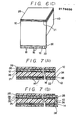
- Figs. 1(A) - l(C) are perspective views illustrating a process for manufacturing a first embodiment of an ultrasonic transducer according to the present invention;
- Figs. 2(A), 2(B) are sectional views taken along lines X-X, Y-Y, respectively, of Fig. l(B);
- Figs. 3(A) - 3(C) are perspective views illustrating a process for manufacturing a second embodiment of an ultrasonic transducer according to the present invention;
- Fig. 4(A) is a sectional view taken along lines Z-Z of Fig. 3(C);
- Fig. 5 is a partially enlarged view illustrating the embodiment of Figs. 3(A) - 3(C);
- Figs. 6(A) - 6(C) are perspective views illustrating a process for manufacturing a third embodiment of an ultrasonic transducer according to the present invention;
- Figs. 7(A), 7(B) are sectional views taken along lines XX-XX, YY-YY, respectively, of Fig. 6(B);
- Figs. 8(A) - 8(D) are perspective views illustrating a process for manufacturing a fourth embodiment of an ultrasonic transducer according to the present invention;
- Fig. 9 is a perspective view illustrating one part of a process for manufacturing a fifth embodiment of an ultrasonic transducer according to the present invention;
- Figs. 10(A) - 10(C) are perspective views illustrating a process for manufacturing an ultrasonic transducer according to the present invention, this being a modification of the embodiment shown in Fig. 1; and
- Figs. ll(A) - ll(D) and 12(A) - 12(D) are perspective views illustrating a polarizing treatment process carried out when a piezoelectric member is to be polarized in advance.
- An ultrasonic transducer according to the present invention and a method of manufacturing the same in accordance with the invention will now be described with reference to the accompanying drawings.
- First, an embodiment in which the present invention is applied to a so-called linear array probe will be described in line with a process, shown in Figs. l(A) - 1(C), for manufacturing the probe. As shown in Fig. l(A), a
piezoelectric member 10 consisting of a piezoelectric polymer material has the form of a flat plate which, in the state shown, is as yet unpolarized. An embodiment in which thepiezoelectric member 10 is polarized in advance will be described in detail later in the specification. The piezoelectric polymer material may comprise polyvinyl fluoride, polyvinylidene fluoride, vinylidene fluoride - vinyl fluoride copolymer, vinylidene fluoride - ethylene trifluoride copolymer, vinylidene fluoride - ethylene tetrafluoride copolymer, vinylidene cyanide - vinyl acetate copolymer, vinylidene cyanide - acrylnitrile copolymer, vinylidene cyanide - vinylidene chloride copolymer, vinylidene cyanide - styrene copolymer, vinylidene cyanide - methyl methacrylate copolymer, vinylidene cyanide - methyl chloro acrylate copolymer, vinylidene cyanide - vinyl benzonate copolymer, vinylidene cyanide - vinyl chloro acetate copolymer, vinylidene cyanide - vinyl chloride copopymer, vinylidene cyanide - acryl acid copolymer, vinylidene cyanide - 2.5-di chloro styrene copolymer, vinylidene cyanide - 2 chloro-1.3-butadiene copolymer, polyvinylidene cyanide, polyacrylnitrile, polyvinyl chloride and the like in molded form, a uniaxially or biaxially stretched material, or a composite obtained by kneading finely divided powder of a strongly dielectric ceramic such as lead zirconate titanate with a polymeric material such as polyvinylidene fluoride, polyvinyl fluoride, nylon, polyacetal or polyacrylnitrile. - A
substrate 12 consists of a flexible insulating material, such as polyimide or polyester, which is molded into the form of a film. Formed integral with thesubstrate 12 on the upper surface thereof in the form of conductive patterns comprising copper foil or the like are anelectrode array 14, a plurality oflead conductors 18, acommon electrode 20, and asingle lead conductor 24. Theelectrode array 14, which serves as a first electrode, comprises a plurality of strip-like electrodes arranged side by side to form an array. Each of thelead conductors 18 has one end connected to a corresponding electrode in theelectrode array 14, and has its other end drawn out to one transverse edge of thesubstrate 12 to form anexternal terminal 16. Thecommon electrode 20, which serves as a second electrode, is disposed adjoining theelectrode array 14 but spaced a prescribed distance therefrom on a region axially symmetric (line 32 serving as the reference) with respect to the region on which theelectrode array 14 is formed. Thelead conductor 24 has one end connected to thecommon electrode 20, and has its other end drawn out to the one transverse edge of thesubstrate 12 to form anexternal terminal 22. One method of forming these conductor patterns on thesubstrate 12 would be to bond a conductive foil, such as the abovementioned copper foil, to the entire surface of thesubstrate 12 by means of an adhesive, and then etch away the foil at the prescribed areas as by photoetching to form the desired patterns. Other well-known methods capable of being applied are vapor deposition and printing. Next, a coating of aninsulative film 26 or the like is applied to the surface of the substrate with the exception of the regions occupied by theelectrode array 14,common electrode 20 andterminals acoustic matching layer 28 is then formed on the underside of thesubstrate 12 on the portion thereof underlying thecommon electrode 20. Also provided on the underside ofsubstrate 12 beneath theterminals strip 30. - Next, an adhesive is applied to the
electrode array 14, thecommon electrode 20, and to the upper surface ofsubstrate 12 at the portion thereof corresponding to thepiezoelectric member 10. As shown in Fig. l(B), thepiezoelectric member 10 is placed upon theelectrode array 14 and thesubstrate 12 is folded upwardly about the line ofsymmetry 32 to bring thecommon electrode 20 into intimate contact with the upper surface of thepiezoelectric member 10. A predetermined amount of pressure accompanied by heating to a prescribed temperature is now applied across theacoustic matching layer 28 and the portion ofsubstrate 12 underlying theelectrode array 14 to set the adhesive. This bonds thepiezoelectric member 10 between theelectrode array 14 and thecommon electrode 20. As shown in the sectional views of Figs. 2(A), 2(B), which are taken along the lines X-X, Y-Y, respectively, of Fig. l(B), anadhesive bond 34 is formed between thepiezoelectric member 10 and theelectrode array 14, and anadhesive bond 36 is formed between thepiezoelectric member 10 and thecommon electrode 20. - The
adhesive bonds electrode array 14 must be insulated from one another. Thus, thebond 34 may be such as exhibits anisotropic conductivity for electrically connecting theelectrode array 14 and the main surface of thepiezoelectric member 10 while at the same time insulating the strip-like electrodes of theelectrode array 14 from one another. In other words, thebond 34 exhibits conductivity in the thickness direction and an insulative property at right angles to the thickness direction. The temperature applied to set the adhesive is 10 to 180°C, preferably 80 to 150°C, the pressure applied is 5 to 80 kg/cm2, preferably 10 to 50 kg/cm2, and the temperature and pressure are applied over a period of time ranging from 1 sec to 10 min, preferably 2 to 30 sec. In Figs. 2(A), 2(B), thenumerals 38 designate adhesive bonds that bond theelectrode array 14, thecommon electrode 20, thelead conductors acoustic matching layer 28 to thesubstrate 12. - After the configuration shown in Fig. l(B) is attained, a voltage is impressed across the
electrode array 14 andcommon electrode 20 via theexternal terminals piezoelectric member 10. Though the polarizing conditions differ depending upon the type of piezoelectric member, exemplary conditions are a temperature of 10 to 180°C, preferably 40 to 175°C, an electric field strength ranging from 50 kV/cm up to the insulation breakdown strength, preferably 100 kV/cm to 2000 kV/cm, and an application time of 10 sec to 10 hr, preferably 10 min to 2 hr. Further, it is essential that the distance from theelectrode array 14 to theexternal terminal 16 and from thecommon electrode 20 to the terminal 22 be so designed as to avoid the occurrence of creepage discharge when the polarizing voltage is applied. - When the polarization of
piezoelectric member 10 is completed, abacking 40 is bonded to the side ofsubstrate 12 underlying theelectrode array 14, after which the portion of thesubstrate 12 carrying thefirst lead conductors 18 is folded onto the side face of thebacking 40. The result is a completed ultrasonic transducer. - According to the first embodiment of the present invention as set forth above, the
electrode array 14, thecommon electrode 20 and thelead conductors piezoelectric member 10 by an adhesive to form a vibrator body. Such a structure and method of manufacture eliminate the need to solder the lead conductors to the electrodes and make it possible to produce the vibrator without subjecting the piezoelectric polymer member to damage caused by heat. - Further, since the electrodes and lead conductors can be substantially connected and the piezoelectric member can be formed while being substantially divided into a plurality of array vibrators in a single manufacturing step, the overall manufacturing process is shortened.
- According to the first embodiment of the present invention, the
electrode array 14 comprising the strip-like electrodes arrayed in side-by-side manner and thecommon electrode 20 opposing theelectrode array 14 are bonded to thepiezoelectric member 10, after which thepiezoelectric member 10 is polarized via theelectrode array 14 andcommon electrode 20. This not only eliminates the need for a prior-art manufacturing step in which the electrode array pattern pitch of the piezoelectric member and the array pattern pitch on the substrate are brought into precise agreement, but also enables an array pattern having a high density to be formed with a high degree of accuracy. - Further, in the above embodiment, the
acoustic matching layer 28 is provided on and integrated with thesubstrate 12, on which the electrodes are formed in advance. Accordingly, theacoustic matching layer 28 can be formed at a predetermined position at the same time as the step for forming the electrodes and lead conductors is performed. - Thus, the first embodiment of the present invention not only shortens the manufacturing process to lower costs but also provides a highly precise, high-density array-type ultrasonic transducer having excellent acoustic characteristics, sensitivity and response.
- More specifically, since the ultrasonic transducer obtained features an acoustic matching layer and adhesive bonds of highly uniform thickness, the characteristics (sensitivity and pulse response) of the individual array vibrators are uniform, so that a uniform ultrasonic tomograph can be produced over a wide field of view. Moreover, the fact that the overall transducer is flexible makes it possible to freely deform the shape of the transducer. Thus, the transducer is applicable not only to linear array probes but also to probes of the arc array and convex array type. Accordingly, a transducer according to the above embodiment of the present invention can be widely applied to various methods of ultrasonic tomography and to the diagnosis of various regions of a living body.
- A second embodiment in which the present invention is applied to a linear array probe will be described in line with a process, shown in Figs. 3(A) - 3(C), for manufacturing the probe. Unlike the embodiment of Figs. l(A) - 1(C), the density of the
electrode array 14 is increased twofold. To achieve this, thelead conductors 18, which are formed integral with respective ones of the strip-like electrodes of theelectrode array 14, are extended alternately to both transverse edges of thesubstrate 12 on either side of theelectrode array 14 to form two sets of theexternal terminals 16, one on each transverse edge, thus assuring that a sufficient spacing is provided between mutually adjacent ones of theterminals 16 on each edge. Thecommon electrode 20 in this embodiment is formed on asubstrate 13 formed projecting from the side surface of theelectrode array 14. The structure and manufacturing method of the ultrasonic transducer of this embodiment are identical with those of the embodiment shown in Figs. l(A) - l(C) in all other respects; hence, identical parts are designated by like reference numerals and are not described again. - Fig. 4 is a sectional view taken along line Z-Z of Fig. 3(C), and Fig. 5 is an enlarged view showing one example of the arrangement of the
electrode array 14 and leadconductors 18. As shown in Fig. 5, each strip-like electrode of theelectrode array 14 has a width of 0.75 mm and a length of 5.0 mm. The spacing between mutually adjacent strip-like electrodes is 0.05 mm. - The embodiment of Figs. 3(A) - 3(C) thus provides an ultrasonic transducer that possesses the advantages of the first embodiment in addition to a higher electrode array density.
- A third embodiment in which the present invention is applied to a linear array probe will be described in line with a process, shown in Figs. 6(A) - 6(C), for manufacturing the probe. Unlike the embodiment of Figs. 1lA) - l(C), the
common electrode 20 is not formed on thesubstrate 12; instead, acommon electrode 21 is formed over the entirety of the main surface ofpiezoelectric member 10 as by vapor deposition of silver or aluminum, and anelectrode contact portion 25 of predetermined width is formed integral with thelead conductor 24 on a position of thesubstrate 12 that will contact a marginal edge portion of thecommon electrode 21 when the portion of thesubstrate 12 provided with theacoustic matching layer 28 is folded onto and bonded to the upper surface of thecommon electrode 21. As shown in the sectional views of Figs. 7(A), 7(B), which are taken along the lines XX-XX, YY-YY, respectively, of Fig. 6(B), theelectrode contact portion 25 is held in intimate pressing contact with the upper surface of the marginal edge portion ofcommon electrode 21 by theadhesive bond 38, thereby effecting an electrical connection between thecontact portion 25 and thecommon electrode 21. The structure and manufacturing method of the ultrasonic transducer of this embodiment are identical with those of the embodiment shown in Figs. l(A) - l(C) in all other respects; hence, identical parts are designated by like reference numerals and are not described again. - Thus, the embodiment of Figs. 6(A) - 6(C) provides an ultrasonic transducer having advantages that supplement those of the first embodiment. Specifically, the electrode contact portion (corresponding to the
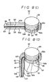
common electrode 20 of Figs. 1(A)), which is formed from a material such as copper foil having a high acoustic impedence, is extremely thin, thecommon electrode 21 is provided on the ultrasonic wave emitting side of the transducer, impedence mismatch between a medium and the vibrator can be diminished, an adverse influence upon the transmission of sent and received waveforms can be reduced. - A fourth embodiment of the present invention shown in figs. 8(A) through 8(D) relates to a manufacturing procedure for forming a circular probe 50. Here a
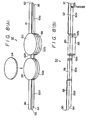
flexible substrate 52 includes twocircular portions piezoelectric polymer member 54, afolding portion 52c linking the twocircular portions conductor support portion 52d extending from thecircular portion 52a, and a leadconductor support portion 52e extending from thecircular portion 52b. An integrally formedfirst electrode 56 andfirst lead conductor 58, coated with a insulator 90 (see Fig. 8(B)), are bonded via an adhesive bond to the substrate surface ofcircular portion 52a and leadconductor support portion 52d, respectively, ofsubstrate 52. Similarly, an integrally formedsecond electrode 60 andsecond lead conductor 60, coated with ainsulator 91, are bonded via an adhesive bond to the substrate surface ofcircular portion 52b and leadconductor support portion 52e, respectively, ofsubstrate 52. The distal end portions of the first and secondlead conductors external terminals substrates acoustic matching layer 68 is provided on the underside ofcircular portion 52b underlying thesecond electrode 20. Next, a coating of an electrically conductive adhesive is applied to the electrode surfaces of the first andsecond electrodes substrate 52 is folded at theportion 52c to bring the first andsecond electrodes piezoelectric member 54 from either side thereof. The bonding conditions and subsequent polarizing treatment are as set forth earlier with regard to the embodiment of Figs. 1(A) - 1(C). The vibrator body formed in this manner is provided with a backingmember 70 bonded thereto, as shown in Fig. 8(D). - The embodiment of Figs. 8(A) - 8(D) has the same advantages as the embodiment of Figs. 1(A) - 1(C).
- Fig. 9 shows a portion of a manufacturing process of a fifth embodiment in which the present invention is applied to a two-dimensional matrix array probe. Unlike the embodiment of Figs. 1(A) - (C), first and second electrodes are provided in the form of
electrode arrays lead conductors flexible substrates electrode arrays piezoelectric member 10 in such a manner that the array directions are perpendicular to each other.Numerals electrode arrays substrate 74 over theelectrode array 74. - The other steps of the manufacturing process are similar to those of the first embodiment and need not be described again. Further, it is possible for the
substrates - The fifth embodiment described above has the same advantages as the embodiment of Figs. 1(A) - l(C).
- Figs. 10(A) - 10(C) show a modification of the embodiment illustrated in Figs. 1(A) - 1(C). This arrangement differs from that of Figs. l(A) - 1(C) in that the flexible substrate is divided into a
substrate 12a for theelectrode array 14 and asubstrate 12b for thecommon electrode 20. - In the embodiments of the invention described hereinabove, the
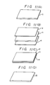
piezoelectric member 10 is subjected to a polarization treatment after being fabricated. Described hereinafter with reference to Figs. ll(A) - ll(D) and 12(A) - 12(D) will be embodiments in which a piezoelectric blank is polarized in advance and then fabricated into thefinal piezoelectric member 10. - The process shown in Figs. ll(A) - 11(D) is for fabricating the
piezoelectric member 10 of Figs. 1(A) - 1(D) from an unpolarized piezoelectric blank 1. Specifically, the unpolarized piezoelectric blank 1 is formed into a flat plate of the type shown in Fig. ll(A), in which state the blank 1 is as yet unpolarized. The piezoelectric blank 1 has a pair of opposing main surfaces, which are the upper and lower surfaces as seen in the drawings. Next, as illustrated in Fig. ll(B), conductive plates (as of copper) 2, 4 are formed on the blank 1 so as to cover the main surfaces, theconductive plates conductive plates polarized piezoelectric member 10, shown in Fig. ll(D). - After the prepolarized vibrator body is thus formed, the
backing 40 is bonded to thesubstrate 12 on the portion underlying theelectrode array 14, and the portion of thesubstrate 12 having the first lead conductors is folded onto the side surface of thebacking 40 to form the ultrasonic transducer, as shown in Fig. l(C). - The process shown in Figs. 12(A) - 12(D) is for fabricating the
piezoelectric member 10 of Figs. 6(A) - 6(D) from the unpolarized piezoelectric blank 1. Unlike the arrangement of Figs. ll(A) - ll(D), theconductive plate 2 is unnecessary since thecommon electrode 21 is formed by a method such as vapor deposition. The structure and manufacturing method are identical with those of the embodiment shown in Figs. 1(A) - l(C) in all other respects; hence, identical parts are designated by like reference numerals and are not described again. - According to the embodiment abovementioned, the
piezoelectric member 10 can be obtained in a large size by applying the polarizing treatment of Figs. 11(A) - ll(D) or Figs. 12(A) - 12(D) to a piezoelectric blank having a large area. By cutting the largepiezoelectric member 10 into pieces of an appropriate size, a large number of piezoelectric members having uniform polarization characteristics (spontaneous polarization) can be obtained at one time. - Thus, according to the ultrasonic transducer and method of manufacture of the present invention as described hereinabove, electrodes or electrode contact portions and lead conductors are formed integral with the same substrate, after which the electrodes or electrode contact portions are bonded to a piezoelectric polymer member or to an electrode formed on the piezoelectric member. Accordingly, it is unnecessary to solder the electrode and leads together, so that a vibrator body can be formed without subjecting the piezoelectric member to damage caused by heat. Moreover, the electrodes and lead conductors can be connected by a single manufacturing step, and the piezoelectric member can be substantially divided into plural array vibrators or into a matrix array vibrator. The manufacturing process can be shortened as a result.
- Further, in a case where electrodes of a predetermined shape are bonded to an unpolarized piezoelectric polymer member followed by polarizing the piezoelectric member through the electrodes, the electrode patterns and the array or matrix array of the piezoelectric member are inevitably in agreement. This makes it possible to form high-density array patterns or the like highly precisely. Conversely, in a case where the a piezoelectric member polarized in advance is used, a large number of ultrasonic transducers having uniform characteristics can be obtained.
- An ultrasonic transducer obtained as set forth above has excellent acoustic characteristics, sensitivity and response (resolution) and can be fabricated to high precision and density. Since the acoustic matching layer and adhesive bonds are uniform in thickness, the characteristics (sensitivity, pulse response) of individual vibrators in an array or matrix array are uniform, thus making it possible to obtain uniform ultrasonic tomographs over a wide field of view. Moreover, the fact that the entire transducer possesses flexibility allows the transducer to be deformed into any shape. Thus, the transducer is not limited to a linear array probe but can be changed into an arc array probe, convex array probe, and the like. Accordingly, the transducer of the present invention has wider applicability in various methods of ultrasonic tomography and can be applied to diagnose more diverse regions of a living body.
- As many apparently widely different embodiments of the present invention can be made without departing from the spirit and scope thereof, it is to be understood that the invention is not limited to the specific embodiments thereof except as defined in the appended claims.
Claims (29)
Applications Claiming Priority (4)
| Application Number | Priority Date | Filing Date | Title |
|---|---|---|---|
| JP59199685A JPH0657080B2 (en) | 1984-09-26 | 1984-09-26 | Ultrasonic probe and method of manufacturing the same |
| JP199685/84 | 1984-09-26 | ||
| JP225126/84 | 1984-10-27 | ||
| JP59225126A JPH0683516B2 (en) | 1984-10-27 | 1984-10-27 | Ultrasonic probe and method of manufacturing the same |
Publications (3)
| Publication Number | Publication Date |
|---|---|
| EP0176030A2 true EP0176030A2 (en) | 1986-04-02 |
| EP0176030A3 EP0176030A3 (en) | 1987-08-05 |
| EP0176030B1 EP0176030B1 (en) | 1992-04-29 |
Family
ID=26511690
Family Applications (1)
| Application Number | Title | Priority Date | Filing Date |
|---|---|---|---|
| EP85111818A Expired - Lifetime EP0176030B1 (en) | 1984-09-26 | 1985-09-18 | Ultrasonic transducer and method of manufacturing same |
Country Status (3)
| Country | Link |
|---|---|
| US (2) | US4701659A (en) |
| EP (1) | EP0176030B1 (en) |
| DE (1) | DE3585938D1 (en) |
Cited By (10)
| Publication number | Priority date | Publication date | Assignee | Title |
|---|---|---|---|---|
| EP0186096A2 (en) * | 1984-12-18 | 1986-07-02 | Kabushiki Kaisha Toshiba | Polymeric piezoelectric ultrasonic probe |
| DE3724290A1 (en) * | 1987-07-22 | 1989-02-02 | Siemens Ag | ELECTRODE FOR PIEZOELECTRIC COMPOSITES |
| EP0420190A2 (en) * | 1989-09-26 | 1991-04-03 | Atochem North America, Inc. | Ultrasonic contact transducer and array |
| EP0426276A2 (en) * | 1989-10-30 | 1991-05-08 | Gec-Marconi Avionics (Holdings) Limited | Transducer testing |
| WO1992018256A1 (en) * | 1991-04-20 | 1992-10-29 | Jones Richard W | Device for acoustic wave generation |
| AU635394B2 (en) * | 1991-02-27 | 1993-03-18 | Bae Systems Avionics Limited | Transducer testing |
| DE19725717A1 (en) * | 1997-06-18 | 1999-02-18 | Hydrometer Gmbh | Ultrasonic transducer for a liquid flowmeter |
| EP1811807A4 (en) * | 2004-10-05 | 2016-09-28 | Ultrasonic transducer | |
| WO2018087560A1 (en) * | 2016-11-11 | 2018-05-17 | University Of The West Of Scotland | Ultrasound transducer |
| DE102017006181A1 (en) * | 2017-06-29 | 2019-01-03 | Diehl Metering Gmbh | Measuring device and method for determining a fluid size |
Families Citing this family (74)
| Publication number | Priority date | Publication date | Assignee | Title |
|---|---|---|---|---|
| US5296777A (en) * | 1987-02-03 | 1994-03-22 | Kabushiki Kaisha Toshiba | Ultrasonic probe |
| DE3803275A1 (en) * | 1988-02-04 | 1989-08-17 | Dornier Medizintechnik | PIEZOELECTRIC SHOCK WAVE SOURCE |
| DE3831975A1 (en) * | 1988-04-12 | 1989-10-26 | Wegu Messtechnik | PIEZO CONTROLLED DYNAMIC PROBE |
| US5111363A (en) * | 1988-06-23 | 1992-05-05 | Teikoku Tsushin Kogyo Co., Ltd. | Mount for electronic parts |
| US5126616A (en) * | 1989-09-05 | 1992-06-30 | Pacesetter Infusion, Ltd. | Ultrasonic transducer electrical interface assembly |
| DE4029262A1 (en) * | 1989-09-16 | 1991-03-28 | Aisin Seiki | POWER SUPPLY DEVICE FOR AN ULTRASONIC VIBRATOR AND VEHICLE MIRROR |
| DE69029938T2 (en) * | 1990-02-28 | 1997-05-28 | Fujitsu Ltd | ULTRASONIC PROBE AND METHOD FOR PRODUCING THE SAME |
| US5222399A (en) * | 1991-02-01 | 1993-06-29 | Fel-Pro Incorporated | Load washer |
| US5155409A (en) * | 1991-07-11 | 1992-10-13 | Caterpillar Inc. | Integral conductor for a piezoelectric actuator |
| US5168189A (en) * | 1991-09-18 | 1992-12-01 | Caterpillar Inc. | Solderless connector for a solid state motor stack |
| US5275167A (en) * | 1992-08-13 | 1994-01-04 | Advanced Technology Laboratories, Inc. | Acoustic transducer with tab connector |
| US5381795A (en) * | 1993-11-19 | 1995-01-17 | Advanced Technology Laboratories, Inc. | Intraoperative ultrasound probe |
| GB9225898D0 (en) * | 1992-12-11 | 1993-02-03 | Univ Strathclyde | Ultrasonic transducer |
| FR2700220B1 (en) * | 1993-01-06 | 1995-02-17 | Saint Louis Inst | Method for polarizing at least one zone of a sheet of ferroelectric material, and method for producing a polarized element for piezoelectric or pyroelectric sensor. |
| US5457863A (en) * | 1993-03-22 | 1995-10-17 | General Electric Company | Method of making a two dimensional ultrasonic transducer array |
| US5412854A (en) * | 1993-06-18 | 1995-05-09 | Humphrey Instruments, Inc. | Method of making a high frequency focused transducer |
| GB2282931B (en) * | 1993-10-16 | 1997-11-12 | Atomic Energy Authority Uk | Flexible transducer array support |
| CA2139151A1 (en) * | 1994-01-14 | 1995-07-15 | Amin M. Hanafy | Two-dimensional acoustic array and method for the manufacture thereof |
| US6420819B1 (en) * | 1994-01-27 | 2002-07-16 | Active Control Experts, Inc. | Packaged strain actuator |
| JP3487981B2 (en) * | 1994-10-20 | 2004-01-19 | オリンパス株式会社 | Ultrasonic probe |
| US6100626A (en) * | 1994-11-23 | 2000-08-08 | General Electric Company | System for connecting a transducer array to a coaxial cable in an ultrasound probe |
| US5563354A (en) * | 1995-04-03 | 1996-10-08 | Force Imaging Technologies, Inc. | Large area sensing cell |
| US5891581A (en) * | 1995-09-07 | 1999-04-06 | The United States Of America As Represented By The Administrator Of The National Aeronautics And Space Administration | Thermally stable, piezoelectric and pyroelectric polymeric substrates |
| DE29623089U1 (en) * | 1996-05-23 | 1997-12-11 | Siemens Ag | Piezoelectric element |
| US5711063A (en) * | 1996-06-11 | 1998-01-27 | Seagate Technology, Inc. | Method of forming a suspension fabricated from silicon |
| US6036813A (en) * | 1996-08-20 | 2000-03-14 | Seagate Technology, Inc. | Method of making anisotropic conductive adhesive interconnects for head attachment in rigid disc drive device for manufacturing a groove bearing |
| US5923115A (en) * | 1996-11-22 | 1999-07-13 | Acuson Corporation | Low mass in the acoustic path flexible circuit interconnect and method of manufacture thereof |
| US5879570A (en) * | 1997-01-14 | 1999-03-09 | Seagate Technology, Inc. | One piece flexure for a hard disc file head with selective nickel plating |
| US6812624B1 (en) | 1999-07-20 | 2004-11-02 | Sri International | Electroactive polymers |
| US5915277A (en) * | 1997-06-23 | 1999-06-22 | General Electric Co. | Probe and method for inspecting an object |
| US6541896B1 (en) * | 1997-12-29 | 2003-04-01 | General Electric Company | Method for manufacturing combined acoustic backing and interconnect module for ultrasonic array |
| FR2779575B1 (en) * | 1998-06-05 | 2003-05-30 | Thomson Csf | MULTI-PIECE ACOUSTIC PROBE COMPRISING A CONDUCTIVE COMPOSITE FILM AND MANUFACTURING METHOD |
| US6286747B1 (en) * | 2000-03-24 | 2001-09-11 | Hong Kong Polytechnic University | Ultrasonic transducer |
| DE10028319A1 (en) * | 2000-06-07 | 2001-12-13 | Endress Hauser Gmbh Co | Electromechanical transducer has piezoelectric elements in stack with intermediate contact electrodes in form of flat connecting vanes fed out of flexible circuit board |
| FR2818170B1 (en) * | 2000-12-19 | 2003-03-07 | Thomson Csf | METHOD OF MANUFACTURING A MULTI-ELEMENT ACOUSTIC PROBE USING A METALLIC AND ABLATE POLYMER FILM AS A GROUND PLAN |
| JP3611796B2 (en) * | 2001-02-28 | 2005-01-19 | 松下電器産業株式会社 | Ultrasonic transducer, manufacturing method of ultrasonic transducer, and ultrasonic flowmeter |
| AU2003225913A1 (en) * | 2002-03-18 | 2003-10-08 | Roy David Kornbluh | Electroactive polymer devices for moving fluid |
| GB2388741B (en) * | 2002-05-17 | 2004-06-30 | Morgan Crucible Co | Transducer assembly |
| WO2004091255A1 (en) * | 2003-04-01 | 2004-10-21 | Olympus Corporation | Ultrasonic vibrator and its manufacturing method |
| US7400513B2 (en) * | 2003-04-22 | 2008-07-15 | Nihon Dempa Kogyo Co., Ltd. | Conductive printed board, multicore cable and ultrasonic probe using the same |
| JP4693386B2 (en) * | 2004-10-05 | 2011-06-01 | 株式会社東芝 | Ultrasonic probe |
| DE602005021604D1 (en) * | 2005-01-18 | 2010-07-15 | Esaote Spa | Ultrasonic probe, in particular for diagnostic imaging |
| US7952261B2 (en) | 2007-06-29 | 2011-05-31 | Bayer Materialscience Ag | Electroactive polymer transducers for sensory feedback applications |
| US20090051250A1 (en) * | 2007-08-21 | 2009-02-26 | Dushyant Shah | Mesh Terminals For Piezoelectric Elements |
| JP5415274B2 (en) * | 2007-10-15 | 2014-02-12 | パナソニック株式会社 | Ultrasonic probe |
| JP5294998B2 (en) * | 2008-06-18 | 2013-09-18 | キヤノン株式会社 | Ultrasonic probe, photoacoustic / ultrasonic system including the ultrasonic probe, and specimen imaging apparatus |
| WO2010044312A1 (en) * | 2008-10-17 | 2010-04-22 | コニカミノルタエムジー株式会社 | Array-type ultrasonic vibrator |
| EP2239793A1 (en) | 2009-04-11 | 2010-10-13 | Bayer MaterialScience AG | Electrically switchable polymer film structure and use thereof |
| US20110109203A1 (en) * | 2009-11-06 | 2011-05-12 | The Trustees Of Princeton University | Flexible piezoelectric structures and method of making same |
| JP5676216B2 (en) * | 2010-11-11 | 2015-02-25 | 日本碍子株式会社 | Method for manufacturing piezoelectric element |
| KR20140008416A (en) | 2011-03-01 | 2014-01-21 | 바이엘 인텔렉쳐 프로퍼티 게엠베하 | Automated manufacturing processes for producing deformable polymer devices and films |
| WO2012129357A2 (en) | 2011-03-22 | 2012-09-27 | Bayer Materialscience Ag | Electroactive polymer actuator lenticular system |
| US8899761B2 (en) | 2011-03-23 | 2014-12-02 | Gentex Corporation | Lens cleaning apparatus |
| JP5406881B2 (en) * | 2011-05-19 | 2014-02-05 | 日立Geニュークリア・エナジー株式会社 | Heat-resistant ultrasonic sensor and installation method thereof |
| US9166141B2 (en) * | 2011-09-09 | 2015-10-20 | Dvx, Llc | Process of manufacturing a piezopolymer transducer with matching layer |
| JP6077813B2 (en) * | 2012-01-23 | 2017-02-08 | 日本電波工業株式会社 | Piezoelectric module |
| JP5713417B2 (en) * | 2012-02-14 | 2015-05-07 | 国立大学法人信州大学 | Gel actuator and manufacturing method thereof |
| EP2828901B1 (en) | 2012-03-21 | 2017-01-04 | Parker Hannifin Corporation | Roll-to-roll manufacturing processes for producing self-healing electroactive polymer devices |
| KR20150031285A (en) | 2012-06-18 | 2015-03-23 | 바이엘 인텔렉쳐 프로퍼티 게엠베하 | Stretch frame for stretching process |
| US9436005B2 (en) | 2012-08-02 | 2016-09-06 | Gentex Corporation | Amplified piezoelectric camera lens cleaner |
| US9590193B2 (en) | 2012-10-24 | 2017-03-07 | Parker-Hannifin Corporation | Polymer diode |
| FR3000213B1 (en) * | 2012-12-21 | 2015-05-15 | Eads Europ Aeronautic Defence | RECONFIGURABLE DEVICE FOR CONTROLLING AN ULTRASONIC COMPOSITE STRUCTURE |
| US10012530B2 (en) | 2013-03-14 | 2018-07-03 | Gentex Corporation | Light sensing device |
| WO2015107932A1 (en) * | 2014-01-20 | 2015-07-23 | 株式会社村田製作所 | Piezoelectric sensor |
| US10514451B2 (en) | 2014-07-15 | 2019-12-24 | Garmin Switzerland Gmbh | Marine sonar display device with three-dimensional views |
| US9812118B2 (en) | 2014-07-15 | 2017-11-07 | Garmin Switzerland Gmbh | Marine multibeam sonar device |
| US9784825B2 (en) | 2014-07-15 | 2017-10-10 | Garmin Switzerland Gmbh | Marine sonar display device with cursor plane |
| US9664783B2 (en) | 2014-07-15 | 2017-05-30 | Garmin Switzerland Gmbh | Marine sonar display device with operating mode determination |
| US9784826B2 (en) | 2014-07-15 | 2017-10-10 | Garmin Switzerland Gmbh | Marine multibeam sonar device |
| US9766328B2 (en) | 2014-07-15 | 2017-09-19 | Garmin Switzerland Gmbh | Sonar transducer array assembly and methods of manufacture thereof |
| US10605913B2 (en) | 2015-10-29 | 2020-03-31 | Garmin Switzerland Gmbh | Sonar noise interference rejection |
| CN110139478B (en) * | 2019-04-02 | 2021-08-13 | 苏州诺莱声科技有限公司 | Method for connecting piezoelectric element with good consistency with flexible circuit board |
| US11619353B2 (en) | 2021-04-06 | 2023-04-04 | Hexagon Technology As | Composite cylinder monitoring system |
| EP4223423A1 (en) * | 2022-02-08 | 2023-08-09 | Nederlandse Organisatie voor toegepast-natuurwetenschappelijk Onderzoek TNO | Acoustic transducer and devices comprising the same |
Citations (4)
| Publication number | Priority date | Publication date | Assignee | Title |
|---|---|---|---|---|
| FR2303436A1 (en) * | 1975-03-03 | 1976-10-01 | Philips Nv | DEVICE FOR CONVERTING ELECTRIC OSCILLATIONS INTO ACOUSTIC VIBRATIONS AND REVERSE, EQUIPPED WITH A MEMBRANE CONTAINING AT LEAST ONE LAYER FORMED BY A PIEZO-ELECTRIC POLYMER |
| GB2052918A (en) * | 1979-06-22 | 1981-01-28 | Consiglio Nazionale Ricerche | Piezoelectric transducers |
| EP0100711A2 (en) * | 1982-07-30 | 1984-02-15 | Thomson-Csf | Half wave transducer using an active piezo-electric polymer element |
| JPS6059899A (en) * | 1983-09-13 | 1985-04-06 | Toshiba Corp | Ultrasonic wave probe |
Family Cites Families (13)
| Publication number | Priority date | Publication date | Assignee | Title |
|---|---|---|---|---|
| JPS5512254B2 (en) * | 1973-07-03 | 1980-03-31 | ||
| GB1530783A (en) * | 1976-01-30 | 1978-11-01 | Emi Ltd | Ultra-sonic pickup device |
| JPS5840805B2 (en) * | 1978-04-10 | 1983-09-08 | 東レ株式会社 | Coordinate input structure |
| JPS5520052A (en) * | 1978-07-28 | 1980-02-13 | Noto Denshi Kogyo Kk | Piezoelectric filter |
| JPS5525278A (en) * | 1978-08-12 | 1980-02-22 | Noto Denshi Kogyo Kk | 3-terminal type piezoelectric filter |
| US4385255A (en) * | 1979-11-02 | 1983-05-24 | Yokogawa Electric Works, Ltd. | Linear array ultrasonic transducer |
| US4281550A (en) * | 1979-12-17 | 1981-08-04 | North American Philips Corporation | Curved array of sequenced ultrasound transducers |
| US4328441A (en) * | 1980-01-31 | 1982-05-04 | Minnesota Mining And Manufacturing Company | Output circuit for piezoelectric polymer pressure sensor |
| DE3019420A1 (en) * | 1980-05-21 | 1981-11-26 | SIEMENS AG AAAAA, 1000 Berlin und 8000 München | METHOD FOR PRODUCING AN ULTRASONIC TRANSDUCER ARRANGEMENT |
| FR2485857B1 (en) * | 1980-06-25 | 1986-05-02 | Commissariat Energie Atomique | MULTI-ELEMENT ULTRASONIC PROBE AND MANUFACTURING METHOD THEREOF |
| JPS5741100A (en) * | 1980-08-23 | 1982-03-06 | Kureha Chem Ind Co Ltd | Ultrasonic probe |
| US4404489A (en) * | 1980-11-03 | 1983-09-13 | Hewlett-Packard Company | Acoustic transducer with flexible circuit board terminals |
| US4479069A (en) * | 1981-11-12 | 1984-10-23 | Hewlett-Packard Company | Lead attachment for an acoustic transducer |
-
1985
- 1985-09-18 US US06/777,284 patent/US4701659A/en not_active Expired - Fee Related
- 1985-09-18 EP EP85111818A patent/EP0176030B1/en not_active Expired - Lifetime
- 1985-09-18 DE DE8585111818T patent/DE3585938D1/en not_active Expired - Fee Related
-
1987
- 1987-03-26 US US07/031,427 patent/US4783888A/en not_active Expired - Fee Related
Patent Citations (4)
| Publication number | Priority date | Publication date | Assignee | Title |
|---|---|---|---|---|
| FR2303436A1 (en) * | 1975-03-03 | 1976-10-01 | Philips Nv | DEVICE FOR CONVERTING ELECTRIC OSCILLATIONS INTO ACOUSTIC VIBRATIONS AND REVERSE, EQUIPPED WITH A MEMBRANE CONTAINING AT LEAST ONE LAYER FORMED BY A PIEZO-ELECTRIC POLYMER |
| GB2052918A (en) * | 1979-06-22 | 1981-01-28 | Consiglio Nazionale Ricerche | Piezoelectric transducers |
| EP0100711A2 (en) * | 1982-07-30 | 1984-02-15 | Thomson-Csf | Half wave transducer using an active piezo-electric polymer element |
| JPS6059899A (en) * | 1983-09-13 | 1985-04-06 | Toshiba Corp | Ultrasonic wave probe |
Non-Patent Citations (1)
| Title |
|---|
| PATENT ABSTRACTS OF JAPAN, vol. 9, no. 193 (E-334)[1916]. 9th August 1985; & JP-A-60 059 899 (TOSHIBA K.K.) 06-04-1985 * |
Cited By (14)
| Publication number | Priority date | Publication date | Assignee | Title |
|---|---|---|---|---|
| EP0186096A2 (en) * | 1984-12-18 | 1986-07-02 | Kabushiki Kaisha Toshiba | Polymeric piezoelectric ultrasonic probe |
| EP0186096A3 (en) * | 1984-12-18 | 1987-10-21 | Kabushiki Kaisha Toshiba | Polymeric piezoelectric ultrasonic probe |
| DE3724290A1 (en) * | 1987-07-22 | 1989-02-02 | Siemens Ag | ELECTRODE FOR PIEZOELECTRIC COMPOSITES |
| EP0420190A3 (en) * | 1989-09-26 | 1992-04-22 | Atochem North America, Inc. | Ultrasonic contact transducer and array |
| EP0420190A2 (en) * | 1989-09-26 | 1991-04-03 | Atochem North America, Inc. | Ultrasonic contact transducer and array |
| EP0426276A2 (en) * | 1989-10-30 | 1991-05-08 | Gec-Marconi Avionics (Holdings) Limited | Transducer testing |
| EP0426276A3 (en) * | 1989-10-30 | 1992-02-12 | The Marconi Company Limited | Transducer testing |
| AU635394B2 (en) * | 1991-02-27 | 1993-03-18 | Bae Systems Avionics Limited | Transducer testing |
| WO1992018256A1 (en) * | 1991-04-20 | 1992-10-29 | Jones Richard W | Device for acoustic wave generation |
| DE19725717A1 (en) * | 1997-06-18 | 1999-02-18 | Hydrometer Gmbh | Ultrasonic transducer for a liquid flowmeter |
| DE19725717C2 (en) * | 1997-06-18 | 2001-08-02 | Hydrometer Gmbh | Ultrasonic transducer for liquid flow meters |
| EP1811807A4 (en) * | 2004-10-05 | 2016-09-28 | Ultrasonic transducer | |
| WO2018087560A1 (en) * | 2016-11-11 | 2018-05-17 | University Of The West Of Scotland | Ultrasound transducer |
| DE102017006181A1 (en) * | 2017-06-29 | 2019-01-03 | Diehl Metering Gmbh | Measuring device and method for determining a fluid size |
Also Published As
| Publication number | Publication date |
|---|---|
| US4701659A (en) | 1987-10-20 |
| US4783888A (en) | 1988-11-15 |
| DE3585938D1 (en) | 1992-06-04 |
| EP0176030B1 (en) | 1992-04-29 |
| EP0176030A3 (en) | 1987-08-05 |
Similar Documents
| Publication | Publication Date | Title |
|---|---|---|
| EP0176030B1 (en) | Ultrasonic transducer and method of manufacturing same | |
| US4704774A (en) | Ultrasonic transducer and method of manufacturing same | |
| JP2502685B2 (en) | Ultrasonic probe manufacturing method | |
| EP0210723B1 (en) | Ultrasonic probe | |
| US20030085635A1 (en) | Multidimensional ultrasonic transducer arrays | |
| JP3210671B2 (en) | Ultrasonic transducer array and its manufacturing method | |
| US5834880A (en) | Multilayer array ultrasonic transducers | |
| EP0872285B1 (en) | Connective backing block for composite transducer | |
| EP1132978B1 (en) | Manufacturing method for a multilayer piezoelectric device and a two-dimensionnally arrayed element packaging structure | |
| EP0167740A2 (en) | Ultrasonic transducer with a multiple-folded piezoelectric polymer film | |
| JPS61144565A (en) | High-polymer piezo-electric type ultrasonic probe | |
| US6558332B1 (en) | Array type ultrasonic probe and a method of manufacturing the same | |
| JP2606249Y2 (en) | Ultrasonic probe | |
| JPS61103399A (en) | Ultrasonic probe and its manufacture | |
| JPS58118739A (en) | Ultasonic probe and production thereof | |
| JP3325368B2 (en) | Ultrasonic probe and manufacturing method thereof | |
| JP3313171B2 (en) | Ultrasonic probe and manufacturing method thereof | |
| JPS6178300A (en) | Ultrasonic probe and manufacturing method thereof | |
| JP4071084B2 (en) | Manufacturing method of two-dimensional array ultrasonic probe | |
| JPS61294998A (en) | Macromolecule piezoelectric type ultrasonic probe | |
| JP3431274B2 (en) | Ultrasonic transducer and manufacturing method thereof | |
| JPH04200096A (en) | Production of ultrasonic probe | |
| JPS63175761A (en) | Ultrasonic probe | |
| JPS6269800A (en) | High molecular piezoelectric type ultrasonic probe | |
| JPH08122310A (en) | Ultrasonic probe |
Legal Events
| Date | Code | Title | Description |
|---|---|---|---|
| PUAI | Public reference made under article 153(3) epc to a published international application that has entered the european phase |
Free format text: ORIGINAL CODE: 0009012 |
|
| 17P | Request for examination filed |
Effective date: 19851015 |
|
| AK | Designated contracting states |
Kind code of ref document: A2 Designated state(s): BE DE FR GB NL |
|
| PUAL | Search report despatched |
Free format text: ORIGINAL CODE: 0009013 |
|
| AK | Designated contracting states |
Kind code of ref document: A3 Designated state(s): BE DE FR GB NL |
|
| 17Q | First examination report despatched |
Effective date: 19900321 |
|
| GRAA | (expected) grant |
Free format text: ORIGINAL CODE: 0009210 |
|
| AK | Designated contracting states |
Kind code of ref document: B1 Designated state(s): BE DE FR GB NL |
|
| REF | Corresponds to: |
Ref document number: 3585938 Country of ref document: DE Date of ref document: 19920604 |
|
| ET | Fr: translation filed | ||
| PLBE | No opposition filed within time limit |
Free format text: ORIGINAL CODE: 0009261 |
|
| STAA | Information on the status of an ep patent application or granted ep patent |
Free format text: STATUS: NO OPPOSITION FILED WITHIN TIME LIMIT |
|
| 26N | No opposition filed | ||
| PGFP | Annual fee paid to national office [announced via postgrant information from national office to epo] |
Ref country code: FR Payment date: 19980909 Year of fee payment: 14 |
|
| PGFP | Annual fee paid to national office [announced via postgrant information from national office to epo] |
Ref country code: DE Payment date: 19980925 Year of fee payment: 14 |
|
| PGFP | Annual fee paid to national office [announced via postgrant information from national office to epo] |
Ref country code: NL Payment date: 19980929 Year of fee payment: 14 |
|
| PGFP | Annual fee paid to national office [announced via postgrant information from national office to epo] |
Ref country code: GB Payment date: 19981001 Year of fee payment: 14 |
|
| PGFP | Annual fee paid to national office [announced via postgrant information from national office to epo] |
Ref country code: BE Payment date: 19981118 Year of fee payment: 14 |
|
| PG25 | Lapsed in a contracting state [announced via postgrant information from national office to epo] |
Ref country code: GB Free format text: LAPSE BECAUSE OF NON-PAYMENT OF DUE FEES Effective date: 19990918 |
|
| PG25 | Lapsed in a contracting state [announced via postgrant information from national office to epo] |
Ref country code: BE Free format text: LAPSE BECAUSE OF NON-PAYMENT OF DUE FEES Effective date: 19990930 |
|
| BERE | Be: lapsed |
Owner name: MITSUBISHI PETROCHEMICAL CO. LTD Effective date: 19990930 Owner name: TERUMO K.K. TRADING AS TERUMO CORP. Effective date: 19990930 |
|
| PG25 | Lapsed in a contracting state [announced via postgrant information from national office to epo] |
Ref country code: NL Free format text: LAPSE BECAUSE OF NON-PAYMENT OF DUE FEES Effective date: 20000401 |
|
| GBPC | Gb: european patent ceased through non-payment of renewal fee |
Effective date: 19990918 |
|
| PG25 | Lapsed in a contracting state [announced via postgrant information from national office to epo] |
Ref country code: FR Free format text: LAPSE BECAUSE OF NON-PAYMENT OF DUE FEES Effective date: 20000531 |
|
| NLV4 | Nl: lapsed or anulled due to non-payment of the annual fee |
Effective date: 20000401 |
|
| PG25 | Lapsed in a contracting state [announced via postgrant information from national office to epo] |
Ref country code: DE Free format text: LAPSE BECAUSE OF NON-PAYMENT OF DUE FEES Effective date: 20000701 |
|
| REG | Reference to a national code |
Ref country code: FR Ref legal event code: ST |