EP0173386B1 - Cmos ram with merged bipolar transistor - Google Patents
Cmos ram with merged bipolar transistor Download PDFInfo
- Publication number
- EP0173386B1 EP0173386B1 EP85201288A EP85201288A EP0173386B1 EP 0173386 B1 EP0173386 B1 EP 0173386B1 EP 85201288 A EP85201288 A EP 85201288A EP 85201288 A EP85201288 A EP 85201288A EP 0173386 B1 EP0173386 B1 EP 0173386B1
- Authority
- EP
- European Patent Office
- Prior art keywords
- transistors
- well
- transistor
- type semiconductor
- semiconductor material
- Prior art date
- Legal status (The legal status is an assumption and is not a legal conclusion. Google has not performed a legal analysis and makes no representation as to the accuracy of the status listed.)
- Expired
Links
Images
Classifications
-
- H—ELECTRICITY
- H01—ELECTRIC ELEMENTS
- H01L—SEMICONDUCTOR DEVICES NOT COVERED BY CLASS H10
- H01L27/00—Devices consisting of a plurality of semiconductor or other solid-state components formed in or on a common substrate
- H01L27/02—Devices consisting of a plurality of semiconductor or other solid-state components formed in or on a common substrate including semiconductor components specially adapted for rectifying, oscillating, amplifying or switching and having at least one potential-jump barrier or surface barrier; including integrated passive circuit elements with at least one potential-jump barrier or surface barrier
- H01L27/04—Devices consisting of a plurality of semiconductor or other solid-state components formed in or on a common substrate including semiconductor components specially adapted for rectifying, oscillating, amplifying or switching and having at least one potential-jump barrier or surface barrier; including integrated passive circuit elements with at least one potential-jump barrier or surface barrier the substrate being a semiconductor body
- H01L27/06—Devices consisting of a plurality of semiconductor or other solid-state components formed in or on a common substrate including semiconductor components specially adapted for rectifying, oscillating, amplifying or switching and having at least one potential-jump barrier or surface barrier; including integrated passive circuit elements with at least one potential-jump barrier or surface barrier the substrate being a semiconductor body including a plurality of individual components in a non-repetitive configuration
- H01L27/07—Devices consisting of a plurality of semiconductor or other solid-state components formed in or on a common substrate including semiconductor components specially adapted for rectifying, oscillating, amplifying or switching and having at least one potential-jump barrier or surface barrier; including integrated passive circuit elements with at least one potential-jump barrier or surface barrier the substrate being a semiconductor body including a plurality of individual components in a non-repetitive configuration the components having an active region in common
- H01L27/0705—Devices consisting of a plurality of semiconductor or other solid-state components formed in or on a common substrate including semiconductor components specially adapted for rectifying, oscillating, amplifying or switching and having at least one potential-jump barrier or surface barrier; including integrated passive circuit elements with at least one potential-jump barrier or surface barrier the substrate being a semiconductor body including a plurality of individual components in a non-repetitive configuration the components having an active region in common comprising components of the field effect type
- H01L27/0711—Devices consisting of a plurality of semiconductor or other solid-state components formed in or on a common substrate including semiconductor components specially adapted for rectifying, oscillating, amplifying or switching and having at least one potential-jump barrier or surface barrier; including integrated passive circuit elements with at least one potential-jump barrier or surface barrier the substrate being a semiconductor body including a plurality of individual components in a non-repetitive configuration the components having an active region in common comprising components of the field effect type in combination with bipolar transistors and diodes, or capacitors, or resistors
- H01L27/0716—Devices consisting of a plurality of semiconductor or other solid-state components formed in or on a common substrate including semiconductor components specially adapted for rectifying, oscillating, amplifying or switching and having at least one potential-jump barrier or surface barrier; including integrated passive circuit elements with at least one potential-jump barrier or surface barrier the substrate being a semiconductor body including a plurality of individual components in a non-repetitive configuration the components having an active region in common comprising components of the field effect type in combination with bipolar transistors and diodes, or capacitors, or resistors in combination with vertical bipolar transistors and diodes, or capacitors, or resistors
-
- H—ELECTRICITY
- H10—SEMICONDUCTOR DEVICES; ELECTRIC SOLID-STATE DEVICES NOT OTHERWISE PROVIDED FOR
- H10B—ELECTRONIC MEMORY DEVICES
- H10B10/00—Static random access memory [SRAM] devices
- H10B10/15—Static random access memory [SRAM] devices comprising a resistor load element
-
- Y—GENERAL TAGGING OF NEW TECHNOLOGICAL DEVELOPMENTS; GENERAL TAGGING OF CROSS-SECTIONAL TECHNOLOGIES SPANNING OVER SEVERAL SECTIONS OF THE IPC; TECHNICAL SUBJECTS COVERED BY FORMER USPC CROSS-REFERENCE ART COLLECTIONS [XRACs] AND DIGESTS
- Y10—TECHNICAL SUBJECTS COVERED BY FORMER USPC
- Y10S—TECHNICAL SUBJECTS COVERED BY FORMER USPC CROSS-REFERENCE ART COLLECTIONS [XRACs] AND DIGESTS
- Y10S257/00—Active solid-state devices, e.g. transistors, solid-state diodes
- Y10S257/903—FET configuration adapted for use as static memory cell
Definitions
- This invention relates to an integrated circuit CMOS static RAM cell, comprising, a substrate of a first conductivity type semiconductor material;
- Such a memory cell is known e.g. from EP-A-0,020,113.
- CMOS Complementary metal oxide semiconductor
- RAM static random access memory
- An integrated circuit CMOS static RAM cell according to the invention is characterized in that there are six regions of said first conductivity type semiconductor material located in said well forming six pockets therein arranged in two sets of three pockets each, the first and third pocket of each set being separated from the second along the surface of said well by sections of said well material comprising four in number;
- One of the features of the invention is the provision of merged NPN bipolar transistors for each cell, which enhances the operation of the cell.
- These NPN-transistors may be fabricated during conventional source/drain diffusions, and by diffusing an N-region into an inherent P-region of the cell. The provision of the NPN transistors consequently does not increase the size of the cell.
- a substrate 11 of a first conductivity or P-type semiconductor material Located in the substrate is a region of a second conductivity or N-type semiconductor material forming a well 13 therein having a surface 15.
- Six regions of P-type semiconductor material are located in well 15. These are identified as Q1 o , Q1 s (Q3 s ), Q3 D (Q5 B ), Q2 o , Q2 s (Q4 s ) and Q4 D (Q6 B ). These regions form six pockets in the well and are arranged in two sets of three pockets each.
- the first pockets Q1 o and Q2 0 and the third pockets Q4 D (Q6 B ) and Q3 D (Q5 B ) of each set are separated from the second pocket Q1 S (Q3 s ) and Q2 s (Q4 s ) along surface 15 of the well by sections of the well material comprising four in number.
- a thin oxide layer (not shown) is formed on the four separating sections of the well. These form insulator layers.
- Gate electrodes of a polysilicon material forming gates Q1 G , Q2 G , Q3 G and Q4 G are formed on the four insulator layers.
- N-type semiconductor material Diffused into the third pocket of each set is a region of N-type semiconductor material.
- These comprise the emitters Q5g and Q6 E of two bipolar transistors of which pockets Q5 8 and Q6 B , form the bases and the N-type well forms the collectors.
- the six regions of P-type material in well 13 and the four gates comprise four field effect transistors Q1, Q2, Q3 and Q4 which are connected as shown in Figure 3.
- Also shown in Figure 3 are two bipolar PNP-type transistors T1 and T2. Each of these is formed on the substrate, as shown in Figure 2 for transistor T1, by diffusing an N well T1 B into the substrate to form the base of its associated transistor.
- the emitter of the associated transistor T1 is formed by the diffusion of a P-type material into the N-well.
- the substrate comprises the collector T1 C of the associated transistor.
- Resistors R1 and R2 may be formed as film devices on substrate 11 in any well known manner.
- transistor Q1 is conductive and transistor Q2 is not-conductive.
- the cell is written into in order to reverse its condition and cause transistor Q1 to be not-conductive and transistor Q2 to be conductive.
- line RA again goes low to turn on transistors Q3 and Q4.
- an appropriate low voltage is applied along line 17 to the base oftransistorT1 to cause it to turn on. This holds line B1 at the low potential of V ss .
- an appropriate voltage is applied along line 19 to the base of transistor T2 to maintain it in its off condition.
- the low voltage on line 17 causes BLto go to low potential V ss since emitter voltage of T1 differs slightly from its collector voltage V ss .
- the base voltage of Q5 is one V be , or about 0.7 V above V ss .
- the voltage of the source of Q3 is just slightly greater than its drain voltage.
- the gate voltage of Q2 is around 1 Volt, i.e. 1V be plus small voltage drops across T1 and Q3 above V ss .
- Q1 and Q2 are assumed to be enhancement FET's with threshold voltages of about 1V. Q2 thus will turn on when its gate voltage drops more than 1 V below V cc .
- V cc is at least 2V (e.g. 5V) above V ss
- applying low voltage on line 17 causes Q2 to turn on because its gate voltage falls to at least 1V below V cc since the gate voltage ofQ2 goes around 1V above V ss .
- Q2 turns on, its drain voltage rises to pull-up the gate divinage of Q1 and causes Q1 to turn off.
Description
- This invention relates to an integrated circuit CMOS static RAM cell, comprising, a substrate of a first conductivity type semiconductor material;
- a region of a second conductivity type semiconductor material located in said substrate and forming a well therein having a surface;
- a plurality of regions of said first conductivity type semiconductor material located in said well, forming source and drain zones of field effect transistors which form two data storage transistors with cross-coupled gate electrodes of the memory cell.
- Such a memory cell is known e.g. from EP-A-0,020,113.
- Complementary metal oxide semiconductor (CMOS) technology is typically employed to fabricate static random access memory (RAM) devices, both N-channel and P-channel memory devices have been designed, in the past, however, in particular P-channel cells have for the most part been considered too slow for practical purposes.
- It is an object of this invention to provide a CMOS static RAM cell, in particular a CMOS N-well, P-channel static RAM cell that is faster than previous cells.
- An integrated circuit CMOS static RAM cell according to the invention is characterized in that there are six regions of said first conductivity type semiconductor material located in said well forming six pockets therein arranged in two sets of three pockets each, the first and third pocket of each set being separated from the second along the surface of said well by sections of said well material comprising four in number;
- a thin oxide layer located on said four sections of said well material forming insulator layers;
- gate electrodes located on said four insulator layers;
- said gate electrodes and said six pockets comprising four field effect transistors, said two data storage transistors and two access transistors;
- one pocket in each set having a region of said second conductivity type semiconductor material located in it, each said region in a pocket comprising the emitter of a bipolar transistor with the pocket it is located in comprising the base and said well comprising the collector of said associated bipolar transistor.
- One of the features of the invention is the provision of merged NPN bipolar transistors for each cell, which enhances the operation of the cell. These NPN-transistors may be fabricated during conventional source/drain diffusions, and by diffusing an N-region into an inherent P-region of the cell. The provision of the NPN transistors consequently does not increase the size of the cell.
- Other objects, features and advantages of the invention will be apparent from the following description and appended claims when considered in conjunction with the accompanying drawing in which:
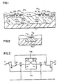
- Figure 1 is a cross-section of the memory cell of the invention;
- Figure 2 is a cross-section of a PNP transistor used in an array of memory cells of the type shown in Figure 1;
- Figure 3 is a circuit diagram of the cell shown in Figure 1 together with two PNP transistors such as that shown in Figure 2.
- Referring now to the drawing, there is shown in Figure 1, a substrate 11 of a first conductivity or P-type semiconductor material. Located in the substrate is a region of a second conductivity or N-type semiconductor material forming a well 13 therein having a
surface 15. Six regions of P-type semiconductor material are located in well 15. These are identified as Q1o, Q1s (Q3s), Q3D (Q5B), Q2o, Q2s (Q4s) and Q4D (Q6B). These regions form six pockets in the well and are arranged in two sets of three pockets each. The first pockets Q1o and Q20 and the third pockets Q4D (Q6B) and Q3D (Q5B) of each set are separated from the second pocket Q1S (Q3s) and Q2s (Q4s) alongsurface 15 of the well by sections of the well material comprising four in number. A thin oxide layer (not shown) is formed on the four separating sections of the well. These form insulator layers. Gate electrodes of a polysilicon material forming gates Q1G, Q2G, Q3G and Q4G are formed on the four insulator layers. - Diffused into the third pocket of each set is a region of N-type semiconductor material. These comprise the emitters Q5g and Q6E of two bipolar transistors of which pockets Q58 and Q6B, form the bases and the N-type well forms the collectors.
- The six regions of P-type material in
well 13 and the four gates comprise four field effect transistors Q1, Q2, Q3 and Q4 which are connected as shown in Figure 3. Also shown in Figure 3 are two bipolar PNP-type transistors T1 and T2. Each of these is formed on the substrate, as shown in Figure 2 for transistor T1, by diffusing an N well T1B into the substrate to form the base of its associated transistor. The emitter of the associated transistor T1 is formed by the diffusion of a P-type material into the N-well. The substrate comprises the collector T1C of the associated transistor. Resistors R1 and R2 (not shown in Figure 1) may be formed as film devices on substrate 11 in any well known manner. - In operation if the cell shown in Figure 3 is to be read, line RA is brought low to turn on transistors Q3 and Q4. Assume the cell to be in such condition that transistor Q1 is charged and transistor Q2 is discharged. When transistor Q3 turns on, transistor Q1 will not conduct and voltage Vcc is not applied to the base of transistor Q5. As a result, that transistor remains in the off condition and line BL remains low. Since transistor Q2 is discharged when transistor Q4 turns on voltage Vcc is applied to the base of transistor Q6 through transistors Q2 and Q4 and transistor Q6 is turned on. As a consequence, Voltage Vcc is applied to line BL to signify that transistor Q2 is uncharged.
- To demonstrate a writing operation assume transistor Q1 is conductive and transistor Q2 is not-conductive. The cell is written into in order to reverse its condition and cause transistor Q1 to be not-conductive and transistor Q2 to be conductive. In order to do this, line RA again goes low to turn on transistors Q3 and Q4. In order to discharge transistor Q1, an appropriate low voltage is applied along
line 17 to the base oftransistorT1 to cause it to turn on. This holds line B1 at the low potential of Vss. At the same time an appropriate voltage is applied alongline 19 to the base of transistor T2 to maintain it in its off condition. - The low voltage on
line 17 causes BLto go to low potential Vss since emitter voltage of T1 differs slightly from its collector voltage Vss. With Q3 (and Q4) turned on, the base voltage of Q5 is one Vbe, or about 0.7 V above Vss. The voltage of the source of Q3 is just slightly greater than its drain voltage. As a result, the gate voltage of Q2 is around 1 Volt, i.e. 1Vbe plus small voltage drops across T1 and Q3 above Vss. Q1 and Q2 are assumed to be enhancement FET's with threshold voltages of about 1V. Q2 thus will turn on when its gate voltage drops more than 1 V below Vcc. Assuming Vcc is at least 2V (e.g. 5V) above Vss, applying low voltage online 17 causes Q2 to turn on because its gate voltage falls to at least 1V below Vcc since the gate voltage ofQ2 goes around 1V above Vss. As Q2 turns on, its drain voltage rises to pull-up the gate voitage of Q1 and causes Q1 to turn off. - As those skilled in the art will appreciate, the arrangement described herein is for illustrative purposes and is not to be considered restrictive.
- Although the invention if of particular importance for P-channel devices, important advantages may be obtained also in N-channel devices wherein Q1, Q2, Q3 and Q4 are provided as N-channel FET's in a P-type well, and wherein the transistors Q5 and Q6 are formed by merged PNP-transistors.
Claims (6)
Applications Claiming Priority (2)
| Application Number | Priority Date | Filing Date | Title |
|---|---|---|---|
| US06/643,580 US4868628A (en) | 1984-08-22 | 1984-08-22 | CMOS RAM with merged bipolar transistor |
| US643580 | 1984-08-22 |
Publications (2)
| Publication Number | Publication Date |
|---|---|
| EP0173386A1 EP0173386A1 (en) | 1986-03-05 |
| EP0173386B1 true EP0173386B1 (en) | 1989-05-03 |
Family
ID=24581420
Family Applications (1)
| Application Number | Title | Priority Date | Filing Date |
|---|---|---|---|
| EP85201288A Expired EP0173386B1 (en) | 1984-08-22 | 1985-08-09 | Cmos ram with merged bipolar transistor |
Country Status (4)
| Country | Link |
|---|---|
| US (1) | US4868628A (en) |
| EP (1) | EP0173386B1 (en) |
| JP (1) | JPS6187361A (en) |
| DE (1) | DE3570017D1 (en) |
Families Citing this family (10)
| Publication number | Priority date | Publication date | Assignee | Title |
|---|---|---|---|---|
| JP2632420B2 (en) * | 1989-02-23 | 1997-07-23 | 三菱電機株式会社 | Semiconductor integrated circuit |
| KR960012252B1 (en) * | 1993-03-05 | 1996-09-18 | 삼성전자 주식회사 | Semiconductor memory device |
| TW372363B (en) * | 1996-04-04 | 1999-10-21 | Mitsubishi Electric Corp | Manufacturing method for static semiconductor memory apparatus and semiconductor apparatus and bipolar transistor |
| JPH1092950A (en) | 1996-09-10 | 1998-04-10 | Mitsubishi Electric Corp | Semiconductor device and manufacture thereof |
| JPH10154393A (en) * | 1996-11-22 | 1998-06-09 | Mitsubishi Electric Corp | Static type semiconductor memory |
| JPH10163435A (en) * | 1996-11-29 | 1998-06-19 | Mitsubishi Electric Corp | Semiconductor memory and manufacture thereof |
| JPH1139877A (en) * | 1997-07-15 | 1999-02-12 | Mitsubishi Electric Corp | Semiconductor storage device |
| JPH1139880A (en) * | 1997-07-16 | 1999-02-12 | Mitsubishi Electric Corp | Semiconductor storage device |
| JPH1139878A (en) * | 1997-07-16 | 1999-02-12 | Mitsubishi Electric Corp | Static type semiconductor memory cell |
| JPH1166858A (en) * | 1997-08-12 | 1999-03-09 | Mitsubishi Electric Corp | Semiconductor storage device |
Family Cites Families (12)
| Publication number | Priority date | Publication date | Assignee | Title |
|---|---|---|---|---|
| DE2460150C2 (en) * | 1974-12-19 | 1984-07-12 | Ibm Deutschland Gmbh, 7000 Stuttgart | Storage arrangement that can be monolithically integrated |
| DE2547220A1 (en) * | 1975-10-22 | 1977-05-05 | Licentia Gmbh | Integrated semiconductor circuit prodn. - deposits semiconductor zones of opposite conductivity in substrate and further zones in first and fourth zones |
| US4150392A (en) * | 1976-07-31 | 1979-04-17 | Nippon Gakki Seizo Kabushiki Kaisha | Semiconductor integrated flip-flop circuit device including merged bipolar and field effect transistors |
| US4125854A (en) * | 1976-12-02 | 1978-11-14 | Mostek Corporation | Symmetrical cell layout for static RAM |
| US4217688A (en) * | 1978-06-12 | 1980-08-19 | Rca Corporation | Fabrication of an integrated injection logic device incorporating an MOS/bipolar current injector |
| JPS5552267A (en) * | 1978-10-11 | 1980-04-16 | Seiko Epson Corp | Semiconductor meomory |
| JPS55101190A (en) * | 1979-01-23 | 1980-08-01 | Fujitsu Ltd | Semiconductor memory device |
| JPS55162260A (en) * | 1979-06-04 | 1980-12-17 | Fujitsu Ltd | Semiconductor ic device |
| JPS5835371B2 (en) * | 1980-01-18 | 1983-08-02 | 松下電器産業株式会社 | semiconductor storage device |
| JPS57186833A (en) * | 1981-05-13 | 1982-11-17 | Hitachi Ltd | Switching element |
| DE3330026A1 (en) * | 1983-08-19 | 1985-02-28 | Siemens AG, 1000 Berlin und 8000 München | INTEGRATED RS FLIPFLOP CIRCUIT |
| DE3330013A1 (en) * | 1983-08-19 | 1985-02-28 | Siemens AG, 1000 Berlin und 8000 München | STATIC STORAGE CELL |
-
1984
- 1984-08-22 US US06/643,580 patent/US4868628A/en not_active Expired - Fee Related
-
1985
- 1985-08-09 DE DE8585201288T patent/DE3570017D1/en not_active Expired
- 1985-08-09 EP EP85201288A patent/EP0173386B1/en not_active Expired
- 1985-08-19 JP JP60181598A patent/JPS6187361A/en active Pending
Also Published As
| Publication number | Publication date |
|---|---|
| US4868628A (en) | 1989-09-19 |
| EP0173386A1 (en) | 1986-03-05 |
| JPS6187361A (en) | 1986-05-02 |
| DE3570017D1 (en) | 1989-06-08 |
Similar Documents
| Publication | Publication Date | Title |
|---|---|---|
| US5350938A (en) | Nonvolatile semiconductor memory circuit with high speed read-out | |
| US4125854A (en) | Symmetrical cell layout for static RAM | |
| US6097641A (en) | High performance DRAM structure employing multiple thickness gate oxide | |
| US5872032A (en) | Fabrication method for a DRAM cell with bipolar charge amplification | |
| EP0245515A1 (en) | Semiconductor device | |
| US20060181919A1 (en) | Embedded DRAM gain memory cell | |
| US6900503B2 (en) | SRAM formed on SOI substrate | |
| GB1571424A (en) | Semiconductor memories | |
| KR19990023762A (en) | Gain Cells for Dynamic Random Access Memory and Bismos Dynamic Random Access Memory Manufacturing Method | |
| GB1419834A (en) | Integrated semiconductor memory cell array | |
| US3979734A (en) | Multiple element charge storage memory cell | |
| EP0173386B1 (en) | Cmos ram with merged bipolar transistor | |
| JPH0766659B2 (en) | Semiconductor memory device | |
| US5285069A (en) | Array of field effect transistors of different threshold voltages in same semiconductor integrated circuit | |
| JP2003030980A (en) | Semiconductor memory | |
| US4253162A (en) | Blocked source node field-effect circuitry | |
| US4791611A (en) | VLSI dynamic memory | |
| US4725875A (en) | Memory cell with diodes providing radiation hardness | |
| JPH06244385A (en) | Static type semiconductor memory device | |
| US5999440A (en) | Embedded DRAM with noise-protecting substrate isolation well | |
| EP0040377A2 (en) | Integrated circuit device for writing and reading information | |
| KR930011463B1 (en) | Semiconductor device | |
| US4506349A (en) | Cross-coupled transistor memory cell for MOS random access memory of reduced power dissipation | |
| KR900001773B1 (en) | The semiconductor integrated circuit | |
| EP0071042B1 (en) | Memory array |
Legal Events
| Date | Code | Title | Description |
|---|---|---|---|
| PUAI | Public reference made under article 153(3) epc to a published international application that has entered the european phase |
Free format text: ORIGINAL CODE: 0009012 |
|
| AK | Designated contracting states |
Kind code of ref document: A1 Designated state(s): DE FR GB |
|
| 17P | Request for examination filed |
Effective date: 19860827 |
|
| 17Q | First examination report despatched |
Effective date: 19880622 |
|
| GRAA | (expected) grant |
Free format text: ORIGINAL CODE: 0009210 |
|
| AK | Designated contracting states |
Kind code of ref document: B1 Designated state(s): DE FR GB |
|
| REF | Corresponds to: |
Ref document number: 3570017 Country of ref document: DE Date of ref document: 19890608 |
|
| ET | Fr: translation filed | ||
| PLBE | No opposition filed within time limit |
Free format text: ORIGINAL CODE: 0009261 |
|
| STAA | Information on the status of an ep patent application or granted ep patent |
Free format text: STATUS: NO OPPOSITION FILED WITHIN TIME LIMIT |
|
| 26N | No opposition filed | ||
| PGFP | Annual fee paid to national office [announced via postgrant information from national office to epo] |
Ref country code: DE Payment date: 19921027 Year of fee payment: 8 |
|
| PGFP | Annual fee paid to national office [announced via postgrant information from national office to epo] |
Ref country code: GB Payment date: 19930730 Year of fee payment: 9 |
|
| PGFP | Annual fee paid to national office [announced via postgrant information from national office to epo] |
Ref country code: FR Payment date: 19930825 Year of fee payment: 9 |
|
| PG25 | Lapsed in a contracting state [announced via postgrant information from national office to epo] |
Ref country code: DE Effective date: 19940503 |
|
| PG25 | Lapsed in a contracting state [announced via postgrant information from national office to epo] |
Ref country code: GB Effective date: 19940809 |
|
| GBPC | Gb: european patent ceased through non-payment of renewal fee |
Effective date: 19940809 |
|
| PG25 | Lapsed in a contracting state [announced via postgrant information from national office to epo] |
Ref country code: FR Effective date: 19950428 |
|
| REG | Reference to a national code |
Ref country code: FR Ref legal event code: ST |