EP0173108B1 - Electrostatic discharge protection circuit with variable limiting threshold for MOS device - Google Patents
Electrostatic discharge protection circuit with variable limiting threshold for MOS device Download PDFInfo
- Publication number
- EP0173108B1 EP0173108B1 EP85109701A EP85109701A EP0173108B1 EP 0173108 B1 EP0173108 B1 EP 0173108B1 EP 85109701 A EP85109701 A EP 85109701A EP 85109701 A EP85109701 A EP 85109701A EP 0173108 B1 EP0173108 B1 EP 0173108B1
- Authority
- EP
- European Patent Office
- Prior art keywords
- input
- potential
- gate
- mos transistor
- protection circuit
- Prior art date
- Legal status (The legal status is an assumption and is not a legal conclusion. Google has not performed a legal analysis and makes no representation as to the accuracy of the status listed.)
- Expired - Lifetime
Links
Images
Classifications
-
- H—ELECTRICITY
- H02—GENERATION; CONVERSION OR DISTRIBUTION OF ELECTRIC POWER
- H02H—EMERGENCY PROTECTIVE CIRCUIT ARRANGEMENTS
- H02H9/00—Emergency protective circuit arrangements for limiting excess current or voltage without disconnection
- H02H9/04—Emergency protective circuit arrangements for limiting excess current or voltage without disconnection responsive to excess voltage
- H02H9/045—Emergency protective circuit arrangements for limiting excess current or voltage without disconnection responsive to excess voltage adapted to a particular application and not provided for elsewhere
- H02H9/046—Emergency protective circuit arrangements for limiting excess current or voltage without disconnection responsive to excess voltage adapted to a particular application and not provided for elsewhere responsive to excess voltage appearing at terminals of integrated circuits
Definitions
- the present invention relates to a semiconductor integrated circuit arrangement
- a semiconductor integrated circuit device containing an input MOS transistor responsive to an input signal, an input terminal, coupled to said input MOS transistor, for receiving said input signal; and an electrostatic discharge protection circuit limiter means coupled to said input MOS transistor and responsive to a given threshold control potential, for limiting at said variable threshold the electrostatic potential applied to the gate of said input MOS transistor, said threshold being variable according to said given threshold control potential.
- EP-A-0 042 305 Another electrostatic protection circuit is known from EP-A-0 042 305, using an MOS transistor connected to ground.
- the transistor is a depletion mode device, so that it conducts when no power is applied. When power is applied, it is switched off and no protection is provided.
- any countermeasure to avoid a faulty application of overvoltage to the gate electrode should be adopted. This is because such a faulty overvoltage application will rupture the electrical insulation of the gate insulation film and result in permanently damaging the MOS semiconductor device with a slight supply of power.
- the gate oxide ruptures when the dielectric strength of the gate oxide, made of e.g. silicon dioxide, is more than approximately 107 V/cm. Thus, if a voltage of 30-50 V is applied across a 300-500 ⁇ thick gate oxide, a rupture occurs. It is conventionally known that such permanent damage can be prevented by providing an input protection circuit which simply suppresses the peak potential of an input voltage below the voltage at which a rupture occurs.
- the semiconductor integrated circuit device initially defined is characterized in that said limiter means includes a bipolar transistor whose emitter-collector path is inserted between the gate of said input MOS transistor and a fixed reference potential and the base of said bipolar transistor is connected to receive said given threshold control potential.
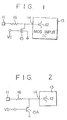
- Fig. 1 shows an electrostatic discharge protection circuit for protecting from overvoltage damage a MOS-input device which is to be responsive to a high-voltage input signal.
- a signal input terminal 11 receives an input signal.
- Terminal 11 is coupled via a resistor element 16 to an input node 14 of a MOS-input semiconductor integrated circuit 13 which contains an input MOS transistor 12 having a gate coupled to node 14.
- Node 14 is coupled to a circuit-ground (substrate) via a gate-controlled MOS diode 15 having a predetermined gate-controlled breakdown voltage (V SB ).
- V SB gate-controlled breakdown voltage
- the gate of the diode 15 receives a power source potential Vc (e.g. 5 volts).
- the potential difference between the gate and drain of MOS diode 15 becomes Vc, because the gate receives potential Vc while the drain potential is substantially zero when no signal is input to terminal 11.
- the gate-controlled breakdown voltage of diode 15 is equivalently increased by Vc from the intrinsic gate-controlled breakdown voltage V SB of MOS diode 15 with zero-gate potential. That is, the limiting threshold for an input signal potential can be made variable according to the gate potential of MOS diode 15, and the responsive potential of the input signal can be set at a high value in proportion to the gate potential.
- the semiconductor integrated circuit device itself at this time an electrostatic discharge is highly liable to occur
- Resistor element 16 between input terminal 11 and input node 14 serves to suppress an excessive input current fed into diode 15 and also to reduce the rate of change of an input signal voltage with a rapid potential change, thereby achieving the protection not only for input MOS transistor 12 but also for gate-controlled MOS diode 15.
- the resistance value of resistor element 16 is preferably 1-2 kohm.
- Fig. 2 shows a circuit configuration of an embodiment of the present invention.
- a PNP bipolar transistor 15A is used in place of the gate-controlled MOS diode.
- the base of transistor 15A is responsive to a fixed or variable base potential Vb.
- Vb base potential
- transistor 15A is rendered conductive so that node 14 is shunted to the circuit ground, thereby achieving the input circuit protection.
- the limiting threshold for the circuit protection is varied by a threshold control potential (Vb) continuously or optionally applied to the base of protection transistor 15A. From this, MOS-input semiconductor circuit 13 is protected from damage due to an excessive high surge voltage input, while no signal blocking is effected for a high-voltage signal input so that semiconductor circuit 13 can respond to such a high-voltage signal input.
- Vb threshold control potential
- MOS-input circuit 13 may include a digital circuit other than EPROM/EEPROM, or it may include a MOS-input analog circuit.
Description
- The present invention relates to a semiconductor integrated circuit arrangement comprising a semiconductor integrated circuit device containing an input MOS transistor responsive to an input signal, an input terminal, coupled to said input MOS transistor, for receiving said input signal; and an electrostatic discharge protection circuit limiter means coupled to said input MOS transistor and responsive to a given threshold control potential, for limiting at said variable threshold the electrostatic potential applied to the gate of said input MOS transistor, said threshold being variable according to said given threshold control potential.
- Such a device is known from IBM Technical Disclosure Bulletin Vol. 22, No. 10, March 1980, pages 4452-4453 in the report entitled, "Voltage Programmable Protect Circuit"
- Another electrostatic protection circuit is known from EP-A-0 042 305, using an MOS transistor connected to ground. The transistor is a depletion mode device, so that it conducts when no power is applied. When power is applied, it is switched off and no protection is provided.
- Generally speaking, for an insulated-gate field effect transistor (MOS transistor) being formed with a metallic gate, insulation film and semiconductor elements, any countermeasure to avoid a faulty application of overvoltage to the gate electrode should be adopted. This is because such a faulty overvoltage application will rupture the electrical insulation of the gate insulation film and result in permanently damaging the MOS semiconductor device with a slight supply of power.
- The gate oxide ruptures when the dielectric strength of the gate oxide, made of e.g. silicon dioxide, is more than approximately 10⁷ V/cm. Thus, if a voltage of 30-50 V is applied across a 300-500 Å thick gate oxide, a rupture occurs. It is conventionally known that such permanent damage can be prevented by providing an input protection circuit which simply suppresses the peak potential of an input voltage below the voltage at which a rupture occurs.
- However, when the above conventional input protection circuit is applied to an ultraviolet erasable non-volatile semiconductor memory (EPROM) or an electric erasable non-volatile semiconductor memory (EEPROM) and, if an input terminal of an EPROM or an EEPROM is designed to be commonly used for a low-voltage signal input and high-voltage signal input (whose potential will not cause said permanent damage), a certain problem arises. That is, when a high-voltage signal is supplied to the input terminal, the input protection circuit with a given fixed input limiting threshold could respond to the potential of a high-voltage input signal so that the necessary high-voltage component exceeding the input limiting threshold is suppressed or blocked. Such inconvenience cannot be avoided according to said conventional input protection circuit.
- It is accordingly an object of the present invention to provide an improved electrostatic discharge protection circuit for protecting from overvoltage damage a MOS-input device which is to be responsive to a high-voltage input signal.
- According to the invention, the semiconductor integrated circuit device initially defined is characterized in that said limiter means includes a bipolar transistor whose emitter-collector path is inserted between the gate of said input MOS transistor and a fixed reference potential and the base of said bipolar transistor is connected to receive said given threshold control potential.
- This invention can be more fully understood from the following detailed description when taken in conjunction with the accompanying drawing, in which:
- Fig. 1 shows a schematic explanatory circuit configuration of a known protection circuit in which a gate-controlled MOS diode with a fixed gate potential is employed; and
- Fig. 2 shows a circuit configuration of an embodiment of the present invention, in which a bipolar transistor with a fixed or variable base potential is employed.
- Fig. 1 shows an electrostatic discharge protection circuit for protecting from overvoltage damage a MOS-input device which is to be responsive to a high-voltage input signal. A signal input terminal 11 receives an input signal. Terminal 11 is coupled via a
resistor element 16 to aninput node 14 of a MOS-input semiconductor integratedcircuit 13 which contains aninput MOS transistor 12 having a gate coupled tonode 14.Node 14 is coupled to a circuit-ground (substrate) via a gate-controlledMOS diode 15 having a predetermined gate-controlled breakdown voltage (VSB). The gate of thediode 15 receives a power source potential Vc (e.g. 5 volts). - According to the circuit of Fig. 1 the potential difference between the gate and drain of
MOS diode 15 becomes Vc, because the gate receives potential Vc while the drain potential is substantially zero when no signal is input to terminal 11. In this case the gate-controlled breakdown voltage ofdiode 15 is equivalently increased by Vc from the intrinsic gate-controlled breakdown voltage VSB ofMOS diode 15 with zero-gate potential. That is, the limiting threshold for an input signal potential can be made variable according to the gate potential ofMOS diode 15, and the responsive potential of the input signal can be set at a high value in proportion to the gate potential. On the other hand, even when the semiconductor integrated circuit device itself is carried (at this time an electrostatic discharge is highly liable to occur), the gate ofinput MOS transistor 12 is protected perfectly. This is because, when carried, no power is supplied to the integrated circuit device so that Vc = 0 and the limiting threshold for the input signal potential is set at a low value which is substantially equal to the intrinsic gate-controlled breakdown voltage ofMOS diode 15 with zero-gate potential. -
Resistor element 16 between input terminal 11 andinput node 14 serves to suppress an excessive input current fed intodiode 15 and also to reduce the rate of change of an input signal voltage with a rapid potential change, thereby achieving the protection not only forinput MOS transistor 12 but also for gate-controlledMOS diode 15. The resistance value ofresistor element 16 is preferably 1-2 kohm. - Fig. 2 shows a circuit configuration of an embodiment of the present invention. In the embodiment of Fig. 2 a PNP
bipolar transistor 15A is used in place of the gate-controlled MOS diode. The base oftransistor 15A is responsive to a fixed or variable base potential Vb. When the potential atinput node 14 exceeds the given base potential Vb of the base-emitter threshold voltage oftransistor 15A,transistor 15A is rendered conductive so thatnode 14 is shunted to the circuit ground, thereby achieving the input circuit protection. - As will be understood from the above description, the limiting threshold for the circuit protection is varied by a threshold control potential (Vb) continuously or optionally applied to the base of
protection transistor 15A. From this, MOS-input semiconductor circuit 13 is protected from damage due to an excessive high surge voltage input, while no signal blocking is effected for a high-voltage signal input so thatsemiconductor circuit 13 can respond to such a high-voltage signal input. - While the invention has been described in connection with what is presently considered to be the most practical and preferred embodiment, it is understood that the invention is not to be limited to the disclosed embodiment. For instance, MOS-
input circuit 13 may include a digital circuit other than EPROM/EEPROM, or it may include a MOS-input analog circuit.
Claims (4)
- A semiconductor integrated circuit arrangement comprising: an integrated circuit device (13) containing an input MOS transistor (12) responsive to an input signal;
an input terminal (11), coupled to said input MOS transistor (12), for receiving said input signal; and
an electrostatic discharge protection circuit comprising: limiter means (15A) coupled to said input MOS transistor (12) and responsive to a given threshold control potential (Vb), for limiting at a variable threshold the electrostatic potential applied to the gate of said input MOS transistor (12), said threshold being variable according to said given threshold control potential (Vb),
characterized in that said limiter means (15A) includes a bipolar transistor (15A) whose emitter-collector path is inserted between the gate of said input MOS transistor (12) and a fixed reference potential and the base of said bipolar transistor (15A) is connected to receive said given threshold control potential (Vb). - A device according to claim 1, characterized in that said given threshold control potential (Vb) corresponds to a power source potential of said semiconductor device (13).
- A device according to claim 1, characterized in that said given threshold control potential (Vb) is higher than a power source potential of said semiconductor device (13).
- A device according to claim 1,2 or 3, characterized in that said limiter means (15A,16) includes a resistor element (16) coupled between said input terminal (11) and said bipolar transistor (15A).
Applications Claiming Priority (2)
| Application Number | Priority Date | Filing Date | Title |
|---|---|---|---|
| JP172559/84 | 1984-08-20 | ||
| JP59172559A JPS6150358A (en) | 1984-08-20 | 1984-08-20 | Semiconductor integrated circuit |
Publications (3)
| Publication Number | Publication Date |
|---|---|
| EP0173108A2 EP0173108A2 (en) | 1986-03-05 |
| EP0173108A3 EP0173108A3 (en) | 1987-07-22 |
| EP0173108B1 true EP0173108B1 (en) | 1993-11-10 |
Family
ID=15944097
Family Applications (1)
| Application Number | Title | Priority Date | Filing Date |
|---|---|---|---|
| EP85109701A Expired - Lifetime EP0173108B1 (en) | 1984-08-20 | 1985-08-02 | Electrostatic discharge protection circuit with variable limiting threshold for MOS device |
Country Status (4)
| Country | Link |
|---|---|
| US (1) | US4692834A (en) |
| EP (1) | EP0173108B1 (en) |
| JP (1) | JPS6150358A (en) |
| DE (1) | DE3587654T2 (en) |
Families Citing this family (35)
| Publication number | Priority date | Publication date | Assignee | Title |
|---|---|---|---|---|
| US4802054A (en) * | 1987-03-13 | 1989-01-31 | Motorola, Inc. | Input protection for an integrated circuit |
| US4855620A (en) * | 1987-11-18 | 1989-08-08 | Texas Instruments Incorporated | Output buffer with improved ESD protection |
| JPH07105446B2 (en) * | 1988-01-11 | 1995-11-13 | 株式会社東芝 | Input protection circuit for MOS semiconductor device |
| US4996626A (en) * | 1988-10-14 | 1991-02-26 | National Semiconductor Corp. | Resistorless electrostatic discharge protection device for high speed integrated circuits |
| US5051604A (en) * | 1989-05-11 | 1991-09-24 | Westinghouse Electric Corp. | Electrically normally closed switch device |
| US5243490A (en) * | 1989-06-28 | 1993-09-07 | Texas Instruments Incorporated | ESD protected FAMOS transistor |
| US5272586A (en) * | 1991-01-29 | 1993-12-21 | National Semiconductor Corporation | Technique for improving ESD immunity |
| US5246872A (en) * | 1991-01-30 | 1993-09-21 | National Semiconductor Corporation | Electrostatic discharge protection device and a method for simultaneously forming MOS devices with both lightly doped and non lightly doped source and drain regions |
| US5208475A (en) * | 1991-01-30 | 1993-05-04 | National Semiconductor Corporation | Electrostatic discharge protection device and a method for simultaneously forming MOS devices with both lightly doped and non lightly doped source and drain regions |
| US5455571A (en) * | 1991-02-11 | 1995-10-03 | Strattec Security Corporation | Fail safe system for a mechanical lock key set with electronic interlock |
| US5287098A (en) * | 1991-02-11 | 1994-02-15 | Briggs & Stratton Corp. | Fail safe system for a mechanical lock and key set with electrical interlock |
| NL9101044A (en) * | 1991-06-17 | 1993-01-18 | Sierra Semiconductor Bv | AC VOLTAGE LIMITER IN MOS TECHNOLOGY. |
| US5255146A (en) * | 1991-08-29 | 1993-10-19 | National Semiconductor Corporation | Electrostatic discharge detection and clamp control circuit |
| US5446320A (en) * | 1992-01-24 | 1995-08-29 | Compaq Computer Corp. | Circuit for clamping power output to ground while the computer is deactivated |
| JP2965840B2 (en) * | 1993-12-02 | 1999-10-18 | 株式会社東芝 | Transistor circuit |
| US5473500A (en) * | 1994-01-13 | 1995-12-05 | Atmel Corporation | Electrostatic discharge circuit for high speed, high voltage circuitry |
| US5553070A (en) * | 1994-09-13 | 1996-09-03 | Riley; Robert E. | Data link module for time division multiplexing control systems |
| US5532178A (en) * | 1995-04-27 | 1996-07-02 | Taiwan Semiconductor Manufacturing Company | Gate process for NMOS ESD protection circuits |
| US5745323A (en) * | 1995-06-30 | 1998-04-28 | Analog Devices, Inc. | Electrostatic discharge protection circuit for protecting CMOS transistors on integrated circuit processes |
| JPH09116023A (en) * | 1995-10-16 | 1997-05-02 | Nec Corp | Input protecting circuit for semiconductor integrated circuit device |
| US5729419A (en) * | 1995-11-20 | 1998-03-17 | Integrated Device Technology, Inc. | Changed device model electrostatic discharge protection circuit for output drivers and method of implementing same |
| US5751525A (en) * | 1996-01-05 | 1998-05-12 | Analog Devices, Inc. | EOS/ESD Protection circuit for an integrated circuit with operating/test voltages exceeding power supply rail voltages |
| US5663678A (en) * | 1996-02-02 | 1997-09-02 | Vanguard International Semiconductor Corporation | ESD protection device |
| US5917689A (en) * | 1996-09-12 | 1999-06-29 | Analog Devices, Inc. | General purpose EOS/ESD protection circuit for bipolar-CMOS and CMOS integrated circuits |
| TW322632B (en) * | 1996-10-14 | 1997-12-11 | Vanguard Int Semiconduct Corp | Electrostatic discharge protection device for integrated circuit input/output port |
| US5838146A (en) * | 1996-11-12 | 1998-11-17 | Analog Devices, Inc. | Method and apparatus for providing ESD/EOS protection for IC power supply pins |
| DE19709717C1 (en) * | 1997-03-10 | 1998-09-24 | Siemens Ag | Piezoelectric fuel injector regulator for IC engine |
| US6624998B2 (en) | 2000-01-24 | 2003-09-23 | Medtronic, Inc. | Electrostatic discharge protection scheme in low potential drop environments |
| US6552886B1 (en) | 2000-06-29 | 2003-04-22 | Pericom Semiconductor Corp. | Active Vcc-to-Vss ESD clamp with hystersis for low supply chips |
| US6958551B2 (en) * | 2002-06-25 | 2005-10-25 | Strattec Security Corporation | Vehicle coded ignition lock using a magnetic sensor |
| AU2002950581A0 (en) * | 2002-08-02 | 2002-09-12 | Wayne Callen | Electrical safety circuit |
| US6898061B1 (en) * | 2003-07-10 | 2005-05-24 | Polarfab, Llc | System and method for dynamic ESD Protection |
| US7750439B2 (en) * | 2005-11-28 | 2010-07-06 | Kabushiki Kaisha Toshiba | ESD protection device |
| US8004807B2 (en) * | 2008-01-31 | 2011-08-23 | Agere Systems Inc. | Overvoltage protection circuit with reduced sensitivity to process variations |
| US20100109053A1 (en) * | 2008-11-04 | 2010-05-06 | Ching-Han Jan | Semiconductor device having integrated circuit with pads coupled by external connecting component and method for modifying integrated circuit |
Family Cites Families (10)
| Publication number | Priority date | Publication date | Assignee | Title |
|---|---|---|---|---|
| NL261262A (en) * | 1960-02-25 | 1900-01-01 | ||
| US3407339A (en) * | 1966-05-02 | 1968-10-22 | North American Rockwell | Voltage protection device utilizing a field effect transistor |
| JPS5530312B2 (en) * | 1975-01-16 | 1980-08-09 | ||
| JPS5299786A (en) * | 1976-02-18 | 1977-08-22 | Agency Of Ind Science & Technol | Mos integrated circuit |
| US4037140A (en) * | 1976-04-14 | 1977-07-19 | Rca Corporation | Protection circuit for insulated-gate field-effect transistors (IGFETS) |
| JPS5563871A (en) * | 1978-11-06 | 1980-05-14 | Nec Corp | Protector for field-effect transistor with insulated gate |
| US4282556A (en) * | 1979-05-21 | 1981-08-04 | Rca Corporation | Input protection device for insulated gate field effect transistor |
| JPS577969A (en) * | 1980-06-18 | 1982-01-16 | Toshiba Corp | Semiconductor integrated circuit |
| JPS583285A (en) * | 1981-06-30 | 1983-01-10 | Fujitsu Ltd | Device for protecting semiconductor integrated circuit |
| US4527213A (en) * | 1981-11-27 | 1985-07-02 | Tokyo Shibaura Denki Kabushiki Kaisha | Semiconductor integrated circuit device with circuits for protecting an input section against an external surge |
-
1984
- 1984-08-20 JP JP59172559A patent/JPS6150358A/en active Pending
-
1985
- 1985-08-02 US US06/761,707 patent/US4692834A/en not_active Expired - Lifetime
- 1985-08-02 DE DE85109701T patent/DE3587654T2/en not_active Expired - Lifetime
- 1985-08-02 EP EP85109701A patent/EP0173108B1/en not_active Expired - Lifetime
Also Published As
| Publication number | Publication date |
|---|---|
| EP0173108A3 (en) | 1987-07-22 |
| EP0173108A2 (en) | 1986-03-05 |
| DE3587654D1 (en) | 1993-12-16 |
| JPS6150358A (en) | 1986-03-12 |
| DE3587654T2 (en) | 1994-04-28 |
| US4692834B1 (en) | 1993-03-02 |
| US4692834A (en) | 1987-09-08 |
Similar Documents
| Publication | Publication Date | Title |
|---|---|---|
| EP0173108B1 (en) | Electrostatic discharge protection circuit with variable limiting threshold for MOS device | |
| US4533970A (en) | Series current limiter | |
| US5838146A (en) | Method and apparatus for providing ESD/EOS protection for IC power supply pins | |
| JPH0237234Y2 (en) | ||
| US4322767A (en) | Bidirectional solid-state protector circuitry using gated diode switches | |
| US5557128A (en) | Insulated-gate type bipolar transistor | |
| EP0248035B1 (en) | Telephone subscriber loop overvoltage protection integrated circuit | |
| ES8404109A1 (en) | Integrated circuit protection device | |
| US5333093A (en) | Protection apparatus for series pass MOSFETS | |
| EP0893867B1 (en) | Resettable overcurrent protective circuit | |
| US4772979A (en) | Voltage shock protection circuit | |
| US5513060A (en) | Series protection circuit | |
| US5986861A (en) | Clamp | |
| US5657195A (en) | Overcurrent protection device | |
| US6064556A (en) | Protection circuit for an electric pulse supply line in a semiconductor integrated device | |
| US4893212A (en) | Protection of power integrated circuits against load voltage surges | |
| EP0802604A2 (en) | Protection circuit | |
| US6069493A (en) | Input circuit and method for protecting the input circuit | |
| US20070146955A1 (en) | Semiconductor integrated circuit device | |
| WO1990014691A1 (en) | Low trigger voltage scr protection device and structure | |
| JPH0548021A (en) | Semiconductor protective circuit | |
| US6169425B1 (en) | Voltage sensing current foldback switch circuit | |
| EP0286739A1 (en) | Transit suppression system | |
| JP3003825B2 (en) | Surge voltage protection circuit | |
| US6452768B1 (en) | Circuit arrangement for protecting integrated circuits against electrostatic discharges |
Legal Events
| Date | Code | Title | Description |
|---|---|---|---|
| PUAI | Public reference made under article 153(3) epc to a published international application that has entered the european phase |
Free format text: ORIGINAL CODE: 0009012 |
|
| 17P | Request for examination filed |
Effective date: 19850802 |
|
| AK | Designated contracting states |
Kind code of ref document: A2 Designated state(s): DE FR GB |
|
| PUAL | Search report despatched |
Free format text: ORIGINAL CODE: 0009013 |
|
| AK | Designated contracting states |
Kind code of ref document: A3 Designated state(s): DE FR GB |
|
| 17Q | First examination report despatched |
Effective date: 19890822 |
|
| RAP1 | Party data changed (applicant data changed or rights of an application transferred) |
Owner name: TOSHIBA INFORMATION SYSTEMS (JAPAN) CORPORATION Owner name: KABUSHIKI KAISHA TOSHIBA |
|
| GRAA | (expected) grant |
Free format text: ORIGINAL CODE: 0009210 |
|
| AK | Designated contracting states |
Kind code of ref document: B1 Designated state(s): DE FR GB |
|
| REF | Corresponds to: |
Ref document number: 3587654 Country of ref document: DE Date of ref document: 19931216 |
|
| ET | Fr: translation filed | ||
| PLBE | No opposition filed within time limit |
Free format text: ORIGINAL CODE: 0009261 |
|
| STAA | Information on the status of an ep patent application or granted ep patent |
Free format text: STATUS: NO OPPOSITION FILED WITHIN TIME LIMIT |
|
| 26N | No opposition filed | ||
| REG | Reference to a national code |
Ref country code: GB Ref legal event code: IF02 |
|
| PGFP | Annual fee paid to national office [announced via postgrant information from national office to epo] |
Ref country code: GB Payment date: 20040728 Year of fee payment: 20 |
|
| PGFP | Annual fee paid to national office [announced via postgrant information from national office to epo] |
Ref country code: FR Payment date: 20040810 Year of fee payment: 20 |
|
| PGFP | Annual fee paid to national office [announced via postgrant information from national office to epo] |
Ref country code: DE Payment date: 20040812 Year of fee payment: 20 |
|
| PG25 | Lapsed in a contracting state [announced via postgrant information from national office to epo] |
Ref country code: GB Free format text: LAPSE BECAUSE OF EXPIRATION OF PROTECTION Effective date: 20050801 |
|
| REG | Reference to a national code |
Ref country code: GB Ref legal event code: PE20 |
|
| APAH | Appeal reference modified |
Free format text: ORIGINAL CODE: EPIDOSCREFNO |