EP0172054A1 - Système d'affichage d'images vidéo sur un écran à balayage ligne par ligne et point par point - Google Patents
Système d'affichage d'images vidéo sur un écran à balayage ligne par ligne et point par point Download PDFInfo
- Publication number
- EP0172054A1 EP0172054A1 EP85401321A EP85401321A EP0172054A1 EP 0172054 A1 EP0172054 A1 EP 0172054A1 EP 85401321 A EP85401321 A EP 85401321A EP 85401321 A EP85401321 A EP 85401321A EP 0172054 A1 EP0172054 A1 EP 0172054A1
- Authority
- EP
- European Patent Office
- Prior art keywords
- memory
- display
- line
- address
- displayed
- Prior art date
- Legal status (The legal status is an assumption and is not a legal conclusion. Google has not performed a legal analysis and makes no representation as to the accuracy of the status listed.)
- Granted
Links
Images


Classifications
-
- G—PHYSICS
- G09—EDUCATION; CRYPTOGRAPHY; DISPLAY; ADVERTISING; SEALS
- G09G—ARRANGEMENTS OR CIRCUITS FOR CONTROL OF INDICATING DEVICES USING STATIC MEANS TO PRESENT VARIABLE INFORMATION
- G09G5/00—Control arrangements or circuits for visual indicators common to cathode-ray tube indicators and other visual indicators
- G09G5/02—Control arrangements or circuits for visual indicators common to cathode-ray tube indicators and other visual indicators characterised by the way in which colour is displayed
- G09G5/022—Control arrangements or circuits for visual indicators common to cathode-ray tube indicators and other visual indicators characterised by the way in which colour is displayed using memory planes
-
- G—PHYSICS
- G09—EDUCATION; CRYPTOGRAPHY; DISPLAY; ADVERTISING; SEALS
- G09G—ARRANGEMENTS OR CIRCUITS FOR CONTROL OF INDICATING DEVICES USING STATIC MEANS TO PRESENT VARIABLE INFORMATION
- G09G5/00—Control arrangements or circuits for visual indicators common to cathode-ray tube indicators and other visual indicators
- G09G5/42—Control arrangements or circuits for visual indicators common to cathode-ray tube indicators and other visual indicators characterised by the display of patterns using a display memory without fixed position correspondence between the display memory contents and the display position on the screen
Definitions
- This invention relates to a display system for video irrages, displayed on a screen by line by line and point by point sweeping, the system being particularly useful for image display in data processing systems including video games, teletext networks, etc..
- FR 83 06 74 1 filed April 25, 1983 by the instant applicant describes such a system which includes a composite memory in which are memorized image data to be displayed for each frame, this memory being connected to a video display processor controlling the screen and to a central processing unit for composing the image in conjunction with the memory, the extraction from the memory of the data relating to the points to be displayed being effected under control of a time base means synchronized with the sweeping.
- the composite memory includes a control memory in which are memorized the data words relating to the information to be displayed on each line of the screen, and a zone memory for memorizing the data relating to the intelligible information to be displayed in certain zones of the screen between one or more pairs of lines.
- the data to be displayed is assembled on the screen from the memorized data by coordination means which are part of the video display processor.
- the size of the composite memory can be considerably reduced, thereby diminishing the number of required integrated circuits.
- An object of this invention is to provide an apparatus of the above type which reduces even further the amount of information which must be memorized for displaying images on a screen.
- This invention therefore relates to a system for the display of video images on a display screen by line by line and point by point frame sweeping, this device including a composite memory in which are memorized image data to be displayed for each frame, this composite memory being connected to a video display processor controlling the screen, to a central processing unit, and to an address processor, for composing the image in conjunction with said memory, the extraction from the memory of the data relating to the points to be displayed being under control of a time base means, syncronized with the screen sweeping, and a control device for dynamic access to the memory for allocating the access times among different units of the system which utilize the memory, said composite memory including, on the one hand, a first control memory for memorizing a data word for a line or a group of lines making up the image to be displayed, each word containing data relating to this line and, on the other hand, a zone memory for the memorization of image data relating exclusively to zones of the image in which intelligible information is to be displayed, means being provided to coordinate, during display,
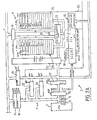
- FIG. 1 shows a very simplified schematic of the visualization system in which the invention is used.
- This system includes a plurality of units as follows:
- the video display processor includes an address processor 10, a point processor 1 for operating on the points of the screen of unit 8, for obtaining, for example, changes in the form of the image, and a display processor 12, these units communicating with each other over time sharing bus 6 and bus 13, on which only data can circulate.
- Buses 6 and 13 are connected to DRAM memory 5 over interface 14 which multiplexes the data and addresses destined for DRAM 5.
- control unit 15 with dynamic access to DRAM memory 5.
- This unit is described in detail in French patent FR -A-2 406 250 and in French patent application n * 83 03 143, filed 25 February 1983, by the instant applicant, and this unit will be referred to, hereinafter, as DMA circuit 15.
- DMA circuit 15 there is provided a time base circuit BT associated with the display processor and communicating with DMA 15, television monitor 8, and the display processor itself.
- CPU 1 communicates with VDP 2 by a single multiplex bus 3 which carries information under control of the signals themselves transmitted on line 4 in such a way that the addresses which are transmitted over this bus can be used, on the one hand, as addresses for DRAM memory 5 when CPU 1 communicates directly with this memory, and by means of which the consecutive data field is utilzed to read or write in the memory, or, on the other hand, as an instruction field placing VDP 2 into a particular configuration for processing the data contained in the consecutive data field.
- the information which passes over bus 3 each have two information fields, the first, enabled by signal AL (address latch), transports either an address for the direct accessing of DRAM 5 or an instruction which is adapted to be interpreted by VDP 2.
- the second field enabled by the signal EN (enable) contains data which traverses the bus in one of two directions, the direction being determined by signal RW (read/write).
- the first field, (address for the memory or interpreted instructions) the data can be sent to the memory or can come from it, or can be utilized by VDP 2 placing it in one of its two processing configurations.
- DRAM 5 in the system here described, is a composite memory having a plurality of zones, addressed starting from a base address.
- This memory is composed of at least a page memory 5a, memories for the control of lines and columns 5b and 5c (see, in this regard, the patent application filed the same day as the instant application in the name of the instant applicant for a "Display System for Video Images on a Screen by Line by Line and Point by Point Sweeping), at least one zone memory 5d, at least one form memory 5e, typographic character memories 5f, a buffer memory 5g, which adapts the various processing speeds to each other, in particular, that of central processing unit - 1 and external channel 9 (see, in this regard, EP-A-00 054 490), and, optionally, a memory 5h programmed in assembly language, for CPU 1, etc..
- All of these memory zones can be accessed by the internal units of VDP 2 and by CPU 1, these accesses being controlled either by the CPU itself or by the device for dynamic access to memory 15 (see, in this regard, FR 83 06 741). In order more easily to understand following description, it is useful briefly to review the operation of DMA circuit 15.
- This circuit distributes access times to DRAM 5 depending upon the priority of the users of the system, that is, CPU 1 and the various units of VDP 2.
- DMA circuit 15 can be requested by each of these users to access the memory, either in a single cycle (monocycle) or in a series of consecutive accesses (multicycle). In this latter case, DMA 15 can control a particular number of accesses to the memory by column access signal (CAS), while utilizing only a single row access signal (RAS).
- CAS column access signal
- RAS single row access signal
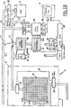
- Interface 7 selectively connects CPU i to VDP 2 for indirect accessing, or to DRAM 5 for direct accessing. It is capable of interpreting each address field.
- the interface 7 includes decoder 16 connected to bus 3 and including 16 outputs, four of which, those corresponding to the two least significant bits, are used to enable four registers of the interface. These registers are:
- Register 23 of interface 7 is loaded with instructions BG when it is designated by an address field, the interpretation of which calls upon one or several background BG cycles.
- a detailed describtion of the operation of interface 7 and the interpretation of instructions FG and BG is in the French patent application filed the same day as the instant application by the instant applicant, entitled Method ans system for the display of visual information on a screen by line by line and point by point video frame sweeping.”
- the address processor besides memory CROM 22, includes two register stacks 24 and 25 called NRAM and PRAM which are loaded and read in 16 bits via transfer register 26 connected to time sharing bus 6. Each stack is connected to arithmetic and logic unit ALU 27, which is itself connected directly to bus 6 by transfer register 26 and to two 16 bit buses 28 and 29, N and P.
- the address processor is used principally to provide and calculate all of the address generated by the VDP for accessing memory 5.
- Memory 22 when it is addressed by a part of the instruction contained either in register 21 FG or in register 23 BG, selects a microinstruction here stored to enable one or more registers of stacks 24 and 25, an arithmetic or logical operation in ALU 27, and transfer by register 26.
- Control memory CROM 22 also provides the signals for the control ing the other units of VDP 2 for the transfer of data and addresses between the various buses and registers.
- the mlcroinstructlons addressed In CR OM 22 are each time enabled in time sharing by DMA 15 on line 30 for establishing a relative priority order for memory accessing. In the case here discussed, six priorities are established in the order:
- Background cycle BG is executed with a lower priority, that is, when VDP 2 does not have other cycles to execute for other users.
- the BG cycle is started either by the CPU by cycle FG, or by VDP 2.
- it is the CPU which starts such a cycle or group of cycles, there can be, for example, a displacement of a group of words in memory 5, this operation being executed without the CPU intervening again after the cycle FG, so that the CPU can continue to process FG during the execution of the BG cycles, all of this being controlled by DMA 15 in the established priority (in this case there will be an interruption and then a restarting of the execution of the BG cycles).
- Interface 14 of DRAM 5 includes two transfer registers 31 and 32 controlled by the signals provided by the microinstructions of memory CROM 22 and by signals RAS and CAS from circuit DMA 15 to transfer the data and address fields of bus 6 to the DRAM or vice versa.
- the data can also be transferred directly into memory 5 from bus 13 to addresses transferred over bus 6 and register 32 from address processor 10.
- the point processor 1 1 includes a 16 word, 16 bit, RAM memory 34, the rows being addressable by addresses YO to YN. It will be appreciated, however, that the point processor could have a much more complex structure to allow veritable manipulations of image elements. In such a case, there could be used the processor described in the patent application filed the same day as the instant application in the name of this applicant and entitled "A POINT PROCESSOR FOR A VIDEO DISPLAY SYSTEM BY LINE BY LINE AND POINT BY POINT FRAME SWEEPING".
- the point processor I also includes address register 35 which can be advance loaded from BG register 23 which down counts its contents by means of signal CAS. This register also controls transfer register 36 by line 37 to transfer the contents of the addresses of RAM 34 on bus 13 when required.
- the display processor (the detailed description of which will follow), includes a set 38 of three digital/analog convertors for converting the five bit time signals (channel RVB) into intensity levels which are used for controlling monitor 8. Thirty-two color levels can be obtained in the example here described.
- the converters 38 are connected to reading outputs of memory 39, called a "color palette", the contents of which being modified in a dynamic manner by CPU 1 as a function of the CPU program.
- memory 39 is loaded from data and address registers 40 and 41 connected to time sharing bus 6.
- RAM memory 39 is addressed by a group 42 of shift registers, the outputs of which being connected to this memory, and the inputs of which, clock CKD (shift rate) being connected to time base BT.
- clock CKD shift rate
- the shifting frequency is equal to the frequency with which the points are displayed on the screen.
- Shift registers 42 can be loaded in two manners, namely, by register group 43, called “plane registers", and by register 44, cal led a "base color register” forming a part of unit 45 for attribute storage.
- Plane registers 43 are loaded from point processor 1 or from DRAM memory 5 by bus 13, and unit 45 is loaded by bus 6, for example, from memory 5 or from CPU 1.
- the operating principle of the display processor is described in FR 83 06 741 as to image display by a control memory in which the composition data for each line to be displayed are stored.
- Figure 4 is a diagram illustrating the utilization of memory planes. This is an abstract concept which allows the illustration of the manner in which the image points are memorized in the page memory.
- Each plane represents a complete visual zone of this screen and is composed of memory cells, one for each image point of the screen.
- the cells are a part of DRAM 5 and can be physically distributed in any manner in the memory network, provided the addresses are known.
- the number of planes used can vary during the display. Assume, for example, that the image is composed of only two colors; in this case, a single memory plane suffices for the first color with "one" bits, and the other color with "zero"bits.
- the memory planes thus defined are associated with a background plane defining the color of the image background.
- This color will appear automatically in the viewable zone. It is coded by an entire frame to be displayed in register 44, the contents of which progress at the rate of the point clock in shift registers 42, unless these are loaded with the contents of plane regsiters 43 when different background Information is to be displayed. It is to be noted that, as the example is a 16 bit system, the extraction from the memory of the color information is effected in 16 bits for 16 image points at a time. It is to be noted also that the contents of the palette memory can vary during operation so that each address code which is applied to the memory does not always correspond to the same color which is actually displayed.
- Figure 5 is a diagram of a video frame on which are inscribed the various operations to be executed for display. It is the time base circuit BT which, from the frame and line syncronization signals, processes all of the required time signals.
- the frame is composed of three concentric zones, that is, the viewable zone at the center, a margin zone, and an exterior compensation zone which for adapting the image definition to all of the known types of monitors and display apparatus.
- the color of the margin zone is defined for each frame in margin register 46 ( Figure 2b) which is enabled only during the display periods of each line corresponding to the margin zone.
- the system utilizes various pointers which form a part of stacks 24 and 25 of address processor 10.
- Figure 6 is a time diagram of the signals generated by time base circuit BT which effect all of the system display modes.
- the first display mode is called “full page”, and consists of memorizing, in DRAM memory 5, all the display information relating to a frame to be displayed, and reading successively, at the corresponding addresses, the point data in one or more color planes. In this mode, the display characteristics do not change during frame display.
- attribute data are memorized in attribute storage unit 45 by corresponding CPU cycles so that this unit will contain the code of the margin color, a base address for addressing the palette memory 39, a number of color planes for the display, and a background color code for the viewable zone.
- each access request REQVISU formed by time base circuit BT and processed by DMA circuit 15 extracts, at the current address PZA, a number of words corresponding to the number of planes programmed into unit 45.
- each request for access REOVISU corresponds to a group of 16 points of the screen. For example, in the present case, as the number of planes selected 1s 4, each access request extracts four words of 16 bits from the memory.
- Each point of the screen is therefore defined by four bits, which, by means of registers 42 and 43, are applied as an address to palette memory 39 at the rate of the point clock for selecting one color among 16.
- the address processor 10 increments pointer PZA upon the extraction of each word from the memory.
- this display mode uses a great deam of memory as each image point is described in a number of bits equal to the number of memory planes selected (for 6 memory planes, there would be required 60K bytes).
- zone memory is therefore loaded in the manner of the page memory, as previously described, with information regarding all the points of only an image zone, all of the other portions of the zone being memorized in the form of words which themselves contain the information regarding all the image points of one or more lines (see FR 83 06 741).
- a part of DRAM memory 5 is organized as a control memory including a first portion in which are stored the words for each frame line, and a second portion in which are stored the data relating to the column parts of the image.
- This control memory is also associated with a zone memory for the intelligible information.
- Figure 8 is a diagram illustrating this display mode called "Graphic Mode by Zone Attributes”.
- a line control memory MGL In this display mode, there are utilized a line control memory MGL, a column control memory MGC, and a zone memory MZ. in this latter memory; the intelligible information of the image are memorized along with one or more color planes.
- the line control memory MGL has as Its function the assembling of the parts of column control memory MGC, this latter assembling the partial pages memories which make up zone memories MZ.
- the circuit of Figures 2a and 2b reconstitutes, from the contents of these memories, the frame under consideration at the moment when the frame appears on the screen.
- the data contained in column control memory MGC includes the attributes to be loaded into storage unit 45 and, if necessary, a zone address PZA which designates the zone to be placed at the corresponding location in the image.
- the attribute data contains the base address of the palette memory, the number of color planes, and the number of accesses to be effected to display the zone.
- the line control memory MGL is successively read for each line during a line syncronization signal.
- This memory includes, for example, 250 words of 16 bits each.
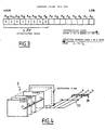
- Figures 9 and 10 illustrate an example of the display of an image on the screen in a graphic display mode by zone attributes.
- the example has eighty lines of the screen representing respectively:
- Region 3 is defined on a single color plane, region 7 on three planes (3 bit code. 8 colors), and region 9 on 6 planes.
- the line control memory MGL contains, for each line, an address pointing to an address of column control memory MGC.
- the attribute ATTRI defines in 16 bits the base color Cl of palette memory 39, the number of color planes (here equal to zero), the number of accesses (here 32 for 512 image points per line).
- the value PGTC2 points to the second line of the column control memory MGC in which the attribute ATTR2 defines the characteristics of region 2.
- This attribute contains the base color information (Cl), the number of planes (0), the number of accesses (5), and the address PZA2 (not utilized) associated with it.
- the pointer PGTC extracts ATTR3 and PZA3, which defines, for region 3, the base color (C2), the number of memory planes (t), the number of accesses (22), and the address of the zone memory MZ where the image data to be displayed are stored.
- the base address of this part of the zone memory is PZA3, and this value is successively incremented for the 22 following accesses for extracting data from the zone memory.
- the line is again displayed in a single color C1.
- Regions 2 to 4 are also presented line by line until line 19, after which region 5 is processed in the same manner as region 1.
- Regions 6 to 10 require, for each line, accesses to the column control memory MGC for the display of the apple and strawberry in a plurality of colors.
- the screen is composed similar to regions 1 and 5.
- the memory size is relatively very small for an image containing a certain quantity of intelligible information.
- this memory size will increase if the intelligible information is increases, but, in most of image sequences, it is rare that this information will extend over more than 50% of the screen.
- the intialization phase of the frame display consists in preparing the contents of the different parts of the DRAM memory controlling display and the VDP2 for the display, namely:
- Each line of "text” includes 27 accesses defined on a - plane and requires 27 words of 16 bits.
- the "0" and "1 bits which define the form are programmed from line >7000.
- the address of the start of the last line is >7195.
- the " apple" is defined on three planes in eight colors. Each line of this zone includes eight accesses, that is, 24 words. The contents of the planes read during the first access of this zone is situated at addresses >B000, >B001, >B002. The address of the beginning of the following line is >B018.
- the "strawberry " is defined on 6 planes in 64 colors, each line of this zone including eight accesses, that is, 48 words. During the first access, the contents of addresses >8000 through >8005 are read and then transferred to display processor 12. The address of the start of the following line is >8030 the address of the start of line 40 is >9008.
- Figure 12 shows that the line control memory MGL selects, according to its contents, the column control zones where are defined the attributes ATTR and the addresses PZA corresponding to the description of the line to be displayed.
- the zones are more or less wide depending upon the display.
- the four first lines of the screen are defined by the sole attribute "ATZI" memorized at address >200, lines 25 to 80 require 5 attribute memorizations for the different zones.
- For each line to be displayed there will be found in the column control memory the addresses of the lines of displayed zones.
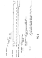
- the display process of the frame is initialized by address "BAGT" - 0000 of the start of the line control memory.
- the 64 emplacements of palette 39 are loaded by color corresponding to the codes memorized in the memory of the display zones.
- the pointer PGTL of line control memory MGL must be initialized by base address BAGT ( Figure 13 and 14).
- the access clock of the time base circuit BT starts during the frame synchronization signal ST and the internal cycle "DMA cycle” which transfers the base address "BAGT” in the pointer PGTL of the line control memory.
- the following accesses relating to the display are triggered during the vertical visualization zone ZVV.
- the display starts with region 1 of four lines defined in a uniform color C1.
- the access request "REO GEST” triggers an access cycle to the line control memory.
- the address >0000 contained in pointer PGTL selected by "NADD" is transferred on bus 6 for loading into interface 14 of the DRAM. During the same period, it is incremented and then reloaded into pointer PGTL.
- the column control pointer PGTC points to the first word of the column control memory from which are extracted the visualization attributes and the address of the zone to be displayed corresponding to the first line displayed of the active zone. This operation is executed from the first access of the horizontal visualization zone ZVH ( Figure 13).
- the first access request REO GEST ( Figure 17 and 18) is generated by time base circuit BT at the start of the horizontal visualization zone ZVH. It starts, by means of DMA 15, a control access utilizing pointer PGTC previously loaded with the value >0200. This access to the column control memory is effected in two cycles, this number being pre-programmed in the attribute register and transferred each GEST cycle into the counter GES CYCLE NB of DMA 15. Each of the two words read is pointed by the value contained in register PGTC.
- pointer PGTC selected by address PADD of memory CROM 22 are, on the one hand, transmitted on bus 6 for loading into address multiplexer 14 of memory 5 (loading signal ALD) and, on the other hand, transferred over bus P29 for incrementing in adder 27 and are reloaded into pointer PGTC.
- the first word read is transferred to attribute register 45 via data bus 13 and bus 6.
- the second word initializes the pointer of the displayed zone PZA selected in stack N 28 by address NADD from CROM 22.
- the attribute of address >200 ATZI defines a base color C i of palette 39, 32 accesses before the first reading of the control memory, that is to say, the complete line, and the number of display planes (0).
- the line control pointer PGTL is equal to >0004. According to the same process, its contents are transferred to pointer P GTC, and are utilized for the first access to the column control memory of this line.
- the address >202 has two definitions corresponding to two zones of the line, namely, a color margin C1 of 5 x 16 points and a text zone defined on a plane of 27 x 16 points.
- the attribute ATZ2 and the address are extracted from the column control memory following the method described above.
- the attribute ATZ2 determines a base color C1 of palette 39 five accesses before the first reading of the column control memory and a number of display planes 0.
- the four accesses do not generate cycle VISU as no memory plane is attributed.
- the color C 1 appears on the screen.
- the time base BT generates a new request REQ GEST which extracts from the column control memory the second attribute controlling the line and address of the display zone.
- the attribute ATTEX ( Figure 12) defines a base color for palette 39, 27 accesses before the next reading of the column control memory, that is, the rest of the line and a number of planes equal to 1.
- the value of PZA >7000 transferred to address processor 10 during the second access GEST is used in the VISU cycle which is started immediately after the access in progress.
- the cycle VISU extracts from the zone memory, at address >7000, the 16 points defining, in a single plane, the start of the text zone.
- the inventive system due to its having a column control memory, also allows the display of typographic Information and the easy mixing in the same frame of graphical and typographical information, it being understood that the system easily accomodates all of the typographic display norms currently in use. (Standards ANTIOPE, CEEFAX, CAPTAIN, BILDSCHIRMTEXT, etc.)
- Figure 19 shows that one can regroup the matrices into two categories A and B, some of them being of the type DRGS (dynamically redefinable character set).
- the matrices of category B cannot be processed with only the form memory because each point is defined by more than two information elements which cannot be translated by a single two state bit.
- each matrix is defined in a plurality of zones of the DRAM memory, namely, in the form memory for character configuration and, in regard to colors, in the column control memory MGC in which are memorized the attributes.
- the display of the characters of category B requires therefore a plurality of consecutive line accesses to DRAM memory 5.
- FIG. 21 there is represented in detail a schematic of the display processor 12 for processing graphical and typographical information.
- Figure 2b shows that the display processor includes a set of registers 43 for memorizing the information of the memory plane. They are loaded with 16 bit words, according to the number of planes to be displayed, under control of logical unit 47.
- the plane registers 43 are connected to shift registers 42 which are loaded when there appears the signal TRANSFERT generated by the control unit 47 in synchronism with the signal REO VISU from DMA 15.
- the shift registers 42 are connected to three multiplexors 48, 49, and 50 for processing the addresses of memory palette 39 as a function of the display mode in progress.
- the multiplexor 48 is used in a graphical mode (as described above), the multiplexor 49 in a typographical mode, and mutliplexor 50 effects the display of the margin color.
- the outputs ADPAL 0 and ADPAL 5 of multiplexors 48, 49, and 50 provide selectively the addresses of the 64 color codes memorized in palette memory 39.
- the multiplexors 48, 49, and 50 are enabled respectively by signals MGEN, MTEN, and CMEN processed in control logical unit 51.
- Attribute memorization unit 45 includes two attribute registers 52 and 53 connected to time sharing bus 6 and providing, in regard to register 52, a margin color code by outputs CM5 to CMO, a number bit CGE1-0 representing the number of accesses per cycle to control memory MG, and bits MCF 5 and MCF 4 for determining the base color of palette memory 39.
- Register 53 also connected to bus 6, provides outputs T and T2 for typographic display, the bits CF5 to CFO determining the background color of the frame and a plane number code represented by bits P2 to P0.
- Register stack 43 is connected to buffer 54 in regard to its eight least significant bits and directly to DRAM bus 13 in regard to its most significant bits.
- Buffer 54 is also connected to DRAM bus 13 and can be .loaded specifically for display in the typographic mode.
- Logical unit 51 is connected to control register 20 ( Figure 2a) of interface 7 for determining the graphical or typographical display mode.
- This register provides signals CMG and CMT, the truth table of which is as follows: operation in the graphical mode is as follows.
- the signal TRANSFERT loads the contents of plane register 43 into shift registers 42.
- the two first cells of multiplexor 48 are enabled.
- Each signal TRANSFERT loads the contents of registers 43 into the respective registers of stack 42, the contents of which being shifted at the rate of signal CKD (point clock) from time base circuit BT.
- Each cell of multiplexor 48 includes an input PL5 to PLO and an input CF5 to CFO and, according to the presence of one of these signals, the image information is converted Into a five bit address of palette memory 39. For example, if four planes are used for the display, signal CILO, 1, 2, and 3 are set at "1 " and signals CTL4 and 5 are at "0". The outputs PLO to PL3 are selected to determine the address of palette memory 39 by outputs ADPALO to ADPAL3 of the cells of multiplexor 48.
- the typographic mode contemplates a plurality of display cases depending on the norms used. These cases are fixed by signals CMG and CMT according to truth table I above, and also as a function of signals T 1 and T2 according to the following truth table.
- Signals CMG and CMT determine if the display is effected with matrices of eight or twelve points per line.
- Signals CMG, CMT, T 1 and T2 are applied to logic unit 5 in which they control the establishment of signals which are applied to multiplexor 49 in the typographic mode.
- signals T1, T2, and CMT are at "0”
- signals MTA3, MTBA1, MTB2, and MTB3 are also at "0”
- signals MTA1 and MTA2 have the value of signal PLO which is the output of the last shift register of stack 42.
- signals MTA3 and MTB3 set at 0, select paths 0 so that signals MCF4 and MCF5, which were previously loaded into attribute register 52, will be applied as base addresses to inputs ADPAL4 and ADPAL5 of palette 39.
- signals MTB1 and MTB2 are at 0 and signals MTA1 and MTA2 have the polarity of signal PL O .
- Each "1" bit of this signal selects the character color of the matrix (CCO to CC3) constituting the address of the palette on inputs ADPALO to ADPAL3.
- Each "0" bit selects the background color (CFO to CF3).
- Figure 22 represents schematically the manner in which the control memory produces the contents of attribute register 53 in the case of an eight bit display.
- register 53 is loaded by the contents of the corresponding cell of column control memory MGC, which contains the four bits CCO to CC3 of the character color, and the - four bits CFO to CF3 of the background color.
- signal CMP is placed at "1" and signal CMG at "0".
- Figure 23 shows the display of some characters having different formats.
- the first matrix concerns a character ISO or DRCS of 12 x 10 points.
- the signals of the background color CFO to CF4 cause the application to palette 39 of an address on inputs ADPALO to ADPAL4.
- signals CCO to CC4 generate the address on these same inputs.
- the signal MCFS from attribute register 52 selects the base color of palette 39.
- the second matrix relates to character DRCS having four colors.
- part 49a selects, with the two-bits PLO and PL 1, a color among four possible colors.
- the column control memory MGC is read at each request REQ VISU and the word READ is loaded into register 53 which contains ( Figure 23) five bits for the background color, five bits for the character color, and bits T and T2.
- the third matrix contains a four color character at half resolution. (Only six points per line.) This resolution is determined by the state of bit T1 (at an up level). In these conditions, the shift registers of stack 42 receive shift signals at half of the point clock frequency (CKD).
- CKD point clock frequency
- multiplexor 49 determines PLO and PHO for the address ADPALO - and ADPAL1, CF2, CF3, CF4, and MCF5 for addresses ADPAL.2 to ADPAL 5.
- This four color address is obtained by successively loading a word of twelve bits from form memory MF into the plane register of stack 43 selected by signal EPR1. During the following access, this word is transferred to the shift register corresponding to stack 42 to generate signals PLO and PHO.
- stack registers 42 and 43 are loaded in two parts, bits BD15 to BD 10 being placed in the right part of the respective registers while buffer 54 toads bits BD9 to BD4 into the left parts.
- PHO appears at the eighth bit of the shift register and PLO at the sixteenth, two information elements, PLO and PHO, shifted at half frequency, select, in palette 39, one color among 4 according to the previously described method.
- the fourth matrix contains a character of type DRCS having 16 colors at half resolution.
- Part 49c of the multiplexor selects CF4 and MCF5 for the base color of palette 39.
- the invention provides for ease in image manipulation, vertical or horizontal, by a simple modification of a frame to another base addresses of the various control memories. It is thus possible to obtain image animation, to load colors, to scroll the image, etc..
Applications Claiming Priority (2)
| Application Number | Priority Date | Filing Date | Title |
|---|---|---|---|
| FR8410374 | 1984-06-29 | ||
| FR8410374A FR2566949B1 (fr) | 1984-06-29 | 1984-06-29 | Systeme d'affichage d'images video sur un ecran a balayage ligne par ligne et point par point |
Publications (2)
| Publication Number | Publication Date |
|---|---|
| EP0172054A1 true EP0172054A1 (fr) | 1986-02-19 |
| EP0172054B1 EP0172054B1 (fr) | 1989-04-12 |
Family
ID=9305640
Family Applications (1)
| Application Number | Title | Priority Date | Filing Date |
|---|---|---|---|
| EP85401321A Expired EP0172054B1 (fr) | 1984-06-29 | 1985-06-28 | Système d'affichage d'images vidéo sur un écran à balayage ligne par ligne et point par point |
Country Status (5)
| Country | Link |
|---|---|
| US (1) | US4827249A (fr) |
| EP (1) | EP0172054B1 (fr) |
| JP (1) | JP2792625B2 (fr) |
| DE (1) | DE3569426D1 (fr) |
| FR (1) | FR2566949B1 (fr) |
Families Citing this family (22)
| Publication number | Priority date | Publication date | Assignee | Title |
|---|---|---|---|---|
| US5243691A (en) * | 1986-06-18 | 1993-09-07 | Hitachi, Ltd. | System for printing documents |
| US4982343A (en) * | 1988-10-11 | 1991-01-01 | Next, Inc. | Method and apparatus for displaying a plurality of graphic images |
| US5235677A (en) * | 1989-06-02 | 1993-08-10 | Atari Corporation | Raster graphics color palette architecture for multiple display objects |
| JPH0731726B2 (ja) * | 1989-06-29 | 1995-04-10 | インターナショナル・ビジネス・マシーンズ・コーポレーシヨン | イメージ処理システム |
| US5210825A (en) * | 1990-04-26 | 1993-05-11 | Teknekron Communications Systems, Inc. | Method and an apparatus for displaying graphical data received from a remote computer by a local computer |
| US5270687A (en) * | 1990-06-27 | 1993-12-14 | Texas Instruments Incorporated | Palette devices, computer graphics systems and method with parallel lookup and input signal splitting |
| US6232955B1 (en) | 1990-06-27 | 2001-05-15 | Texas Instruments Incorporated | Palette devices, systems and methods for true color mode |
| US5309551A (en) * | 1990-06-27 | 1994-05-03 | Texas Instruments Incorporated | Devices, systems and methods for palette pass-through mode |
| US5293468A (en) * | 1990-06-27 | 1994-03-08 | Texas Instruments Incorporated | Controlled delay devices, systems and methods |
| US5327159A (en) * | 1990-06-27 | 1994-07-05 | Texas Instruments Incorporated | Packed bus selection of multiple pixel depths in palette devices, systems and methods |
| US5341470A (en) * | 1990-06-27 | 1994-08-23 | Texas Instruments Incorporated | Computer graphics systems, palette devices and methods for shift clock pulse insertion during blanking |
| US5717697A (en) * | 1990-06-27 | 1998-02-10 | Texas Instruments Incorporated | Test circuits and methods for integrated circuit having memory and non-memory circuits by accumulating bits of a particular logic state |
| US5546553A (en) * | 1990-09-24 | 1996-08-13 | Texas Instruments Incorporated | Multifunctional access devices, systems and methods |
| US5699087A (en) * | 1991-06-24 | 1997-12-16 | Texas Instruments | Sequential access memories, systems and methods |
| US5838389A (en) * | 1992-11-02 | 1998-11-17 | The 3Do Company | Apparatus and method for updating a CLUT during horizontal blanking |
| US5481275A (en) | 1992-11-02 | 1996-01-02 | The 3Do Company | Resolution enhancement for video display using multi-line interpolation |
| US5596693A (en) * | 1992-11-02 | 1997-01-21 | The 3Do Company | Method for controlling a spryte rendering processor |
| US5572235A (en) * | 1992-11-02 | 1996-11-05 | The 3Do Company | Method and apparatus for processing image data |
| US5752073A (en) * | 1993-01-06 | 1998-05-12 | Cagent Technologies, Inc. | Digital signal processor architecture |
| US5398316A (en) * | 1993-02-16 | 1995-03-14 | Texas Instruments Incorporated | Devices, systems and methods for accessing data using a pixel preferred data organization |
| US7313764B1 (en) * | 2003-03-06 | 2007-12-25 | Apple Inc. | Method and apparatus to accelerate scrolling for buffered windows |
| FR2896075B1 (fr) * | 2006-01-10 | 2008-05-16 | Thales Sa | Dispositif et procede d'affichage de symboles statiques sur un ecran matriciel |
Citations (3)
| Publication number | Priority date | Publication date | Assignee | Title |
|---|---|---|---|---|
| US4074254A (en) * | 1976-07-22 | 1978-02-14 | International Business Machines Corporation | Xy addressable and updateable compressed video refresh buffer for digital tv display |
| FR2386868A1 (fr) * | 1977-04-06 | 1978-11-03 | Texas Instruments Inc | Dispositif d'affichage de caracteres et d'informations graphiques sur un ecran d'image en couleurs |
| FR2492618A1 (fr) * | 1980-10-16 | 1982-04-23 | Sony Corp | Appareil d'affichage d'informations en couleurs |
Family Cites Families (8)
| Publication number | Priority date | Publication date | Assignee | Title |
|---|---|---|---|---|
| US3591842A (en) * | 1966-09-01 | 1971-07-06 | Wenczler & Heidenhain | Grid with graduation markings succeeding in nonequidistant spaces relative to each other |
| JPS5454531A (en) * | 1977-10-11 | 1979-04-28 | Hitachi Ltd | Crt display unti |
| US4203107A (en) * | 1978-11-08 | 1980-05-13 | Zentec Corporation | Microcomputer terminal system having a list mode operation for the video refresh circuit |
| GB2038596B (en) * | 1978-12-20 | 1982-12-08 | Ibm | Raster display apparatus |
| US4249172A (en) * | 1979-09-04 | 1981-02-03 | Honeywell Information Systems Inc. | Row address linking control system for video display terminal |
| EP0059349B1 (fr) * | 1981-02-23 | 1986-08-06 | Texas Instruments Incorporated | Système d'affichage divisé en plusieurs zônes avec décalage de texte par zône |
| FR2535871B1 (fr) * | 1982-11-04 | 1987-06-19 | Vigarie Jean Pierre | Terminal graphique a memoire de points muni d'un systeme d'ecriture en memoire d'image de signaux de texture d'image |
| US4555802A (en) * | 1983-01-10 | 1985-11-26 | International Business Machines Corporation | Compaction and decompaction of non-coded information bearing signals |
-
1984
- 1984-06-29 FR FR8410374A patent/FR2566949B1/fr not_active Expired
-
1985
- 1985-06-28 DE DE8585401321T patent/DE3569426D1/de not_active Expired
- 1985-06-28 JP JP60142378A patent/JP2792625B2/ja not_active Expired - Fee Related
- 1985-06-28 EP EP85401321A patent/EP0172054B1/fr not_active Expired
-
1987
- 1987-08-05 US US07/082,965 patent/US4827249A/en not_active Expired - Lifetime
Patent Citations (3)
| Publication number | Priority date | Publication date | Assignee | Title |
|---|---|---|---|---|
| US4074254A (en) * | 1976-07-22 | 1978-02-14 | International Business Machines Corporation | Xy addressable and updateable compressed video refresh buffer for digital tv display |
| FR2386868A1 (fr) * | 1977-04-06 | 1978-11-03 | Texas Instruments Inc | Dispositif d'affichage de caracteres et d'informations graphiques sur un ecran d'image en couleurs |
| FR2492618A1 (fr) * | 1980-10-16 | 1982-04-23 | Sony Corp | Appareil d'affichage d'informations en couleurs |
Also Published As
| Publication number | Publication date |
|---|---|
| US4827249A (en) | 1989-05-02 |
| EP0172054B1 (fr) | 1989-04-12 |
| FR2566949B1 (fr) | 1986-12-26 |
| JPS61193193A (ja) | 1986-08-27 |
| JP2792625B2 (ja) | 1998-09-03 |
| FR2566949A1 (fr) | 1986-01-03 |
| DE3569426D1 (en) | 1989-05-18 |
Similar Documents
| Publication | Publication Date | Title |
|---|---|---|
| EP0172054B1 (fr) | Système d'affichage d'images vidéo sur un écran à balayage ligne par ligne et point par point | |
| EP0172055B1 (fr) | Procédé et système pour l'affichage d'informations visuelles sur un écran par balayage ligne par ligne et point par point de trames vidéo | |
| US4768157A (en) | Video image processing system | |
| US4620289A (en) | Video display system | |
| US4868557A (en) | Video display apparatus | |
| US5043714A (en) | Video display apparatus | |
| CA1148285A (fr) | Dispositif d'affichage de trame | |
| US4618858A (en) | Information display system having a multiple cell raster scan display | |
| CA1053816A (fr) | Generateur de caracteres a grande resolution | |
| US5038300A (en) | Extendable-size color look-up table for computer graphics systems | |
| EP0279229B1 (fr) | Système de visualisation graphique | |
| US5815137A (en) | High speed display system having cursor multiplexing scheme | |
| US4800380A (en) | Multi-plane page mode video memory controller | |
| US4616220A (en) | Graphics display comparator for multiple bit plane graphics controller | |
| US4744046A (en) | Video display terminal with paging and scrolling | |
| EP0279225B1 (fr) | Compteurs à configuration variable pour l'adressage dans les systèmes de visualisation graphiques | |
| JPS62248030A (ja) | ラスタ走査ビデオ制御装置において更新プロセスと表示プロセスとの間で表示メモリをプログラム可能に振り分ける装置 | |
| US4816817A (en) | Line mover for bit-mapped display | |
| EP0279227A2 (fr) | Générateur de tracé de vecteur pour l'affichage vidéo à balayage par trame | |
| JPH06100958B2 (ja) | 表示装置 | |
| EP0225197B1 (fr) | Dispositif de commande d'affichage vidéo | |
| US4626839A (en) | Programmable video display generator | |
| EP0121453B1 (fr) | Système de visualisation de données sur un écran vidéo en mode graphique | |
| US5379408A (en) | Color palette timing and control with circuitry for producing an additional clock cycle during a clock disabled time period | |
| EP0279231B1 (fr) | Processeur d'affichage vidéo en mode graphique pour un système d'affichage vidéo à haute performance |
Legal Events
| Date | Code | Title | Description |
|---|---|---|---|
| PUAI | Public reference made under article 153(3) epc to a published international application that has entered the european phase |
Free format text: ORIGINAL CODE: 0009012 |
|
| AK | Designated contracting states |
Designated state(s): DE FR GB NL |
|
| 17P | Request for examination filed |
Effective date: 19860801 |
|
| 17Q | First examination report despatched |
Effective date: 19880819 |
|
| GRAA | (expected) grant |
Free format text: ORIGINAL CODE: 0009210 |
|
| AK | Designated contracting states |
Kind code of ref document: B1 Designated state(s): DE FR GB NL |
|
| PG25 | Lapsed in a contracting state [announced via postgrant information from national office to epo] |
Ref country code: NL Effective date: 19890412 |
|
| REF | Corresponds to: |
Ref document number: 3569426 Country of ref document: DE Date of ref document: 19890518 |
|
| ET | Fr: translation filed | ||
| NLV1 | Nl: lapsed or annulled due to failure to fulfill the requirements of art. 29p and 29m of the patents act | ||
| PLBE | No opposition filed within time limit |
Free format text: ORIGINAL CODE: 0009261 |
|
| STAA | Information on the status of an ep patent application or granted ep patent |
Free format text: STATUS: NO OPPOSITION FILED WITHIN TIME LIMIT |
|
| 26N | No opposition filed | ||
| PGFP | Annual fee paid to national office [announced via postgrant information from national office to epo] |
Ref country code: GB Payment date: 20010502 Year of fee payment: 17 |
|
| PGFP | Annual fee paid to national office [announced via postgrant information from national office to epo] |
Ref country code: FR Payment date: 20010531 Year of fee payment: 17 |
|
| PGFP | Annual fee paid to national office [announced via postgrant information from national office to epo] |
Ref country code: DE Payment date: 20010627 Year of fee payment: 17 |
|
| REG | Reference to a national code |
Ref country code: GB Ref legal event code: IF02 |
|
| PG25 | Lapsed in a contracting state [announced via postgrant information from national office to epo] |
Ref country code: GB Free format text: LAPSE BECAUSE OF NON-PAYMENT OF DUE FEES Effective date: 20020628 |
|
| PG25 | Lapsed in a contracting state [announced via postgrant information from national office to epo] |
Ref country code: DE Free format text: LAPSE BECAUSE OF NON-PAYMENT OF DUE FEES Effective date: 20030101 |
|
| GBPC | Gb: european patent ceased through non-payment of renewal fee |
Effective date: 20020628 |
|
| PG25 | Lapsed in a contracting state [announced via postgrant information from national office to epo] |
Ref country code: FR Free format text: LAPSE BECAUSE OF NON-PAYMENT OF DUE FEES Effective date: 20030228 |
|
| REG | Reference to a national code |
Ref country code: FR Ref legal event code: ST |