EP0171322B1 - Electric device or circuit testing method and apparatus - Google Patents
Electric device or circuit testing method and apparatus Download PDFInfo
- Publication number
- EP0171322B1 EP0171322B1 EP85401474A EP85401474A EP0171322B1 EP 0171322 B1 EP0171322 B1 EP 0171322B1 EP 85401474 A EP85401474 A EP 85401474A EP 85401474 A EP85401474 A EP 85401474A EP 0171322 B1 EP0171322 B1 EP 0171322B1
- Authority
- EP
- European Patent Office
- Prior art keywords
- measurements
- response
- measurement
- difference
- value
- Prior art date
- Legal status (The legal status is an assumption and is not a legal conclusion. Google has not performed a legal analysis and makes no representation as to the accuracy of the status listed.)
- Expired - Lifetime
Links
- 238000012360 testing method Methods 0.000 title claims description 34
- 238000005259 measurement Methods 0.000 claims description 92
- 230000004044 response Effects 0.000 claims description 42
- 238000000034 method Methods 0.000 claims description 22
- 230000000063 preceeding effect Effects 0.000 claims 1
- 230000004936 stimulating effect Effects 0.000 claims 1
- 239000011159 matrix material Substances 0.000 description 9
- 239000000523 sample Substances 0.000 description 9
- 238000004364 calculation method Methods 0.000 description 7
- 238000010586 diagram Methods 0.000 description 5
- 230000006870 function Effects 0.000 description 5
- 230000002950 deficient Effects 0.000 description 2
- 238000013461 design Methods 0.000 description 2
- 230000008569 process Effects 0.000 description 2
- 238000012545 processing Methods 0.000 description 2
- 230000009467 reduction Effects 0.000 description 2
- 238000010998 test method Methods 0.000 description 2
- 230000002159 abnormal effect Effects 0.000 description 1
- 230000001133 acceleration Effects 0.000 description 1
- 230000008901 benefit Effects 0.000 description 1
- 238000009529 body temperature measurement Methods 0.000 description 1
- 239000003990 capacitor Substances 0.000 description 1
- 230000001419 dependent effect Effects 0.000 description 1
- 230000000977 initiatory effect Effects 0.000 description 1
- 238000011835 investigation Methods 0.000 description 1
- 238000012986 modification Methods 0.000 description 1
- 230000004048 modification Effects 0.000 description 1
- 238000005070 sampling Methods 0.000 description 1
- 238000012163 sequencing technique Methods 0.000 description 1
- 230000001052 transient effect Effects 0.000 description 1
Images



Classifications
-
- G—PHYSICS
- G01—MEASURING; TESTING
- G01R—MEASURING ELECTRIC VARIABLES; MEASURING MAGNETIC VARIABLES
- G01R31/00—Arrangements for testing electric properties; Arrangements for locating electric faults; Arrangements for electrical testing characterised by what is being tested not provided for elsewhere
- G01R31/28—Testing of electronic circuits, e.g. by signal tracer
- G01R31/2832—Specific tests of electronic circuits not provided for elsewhere
- G01R31/2834—Automated test systems [ATE]; using microprocessors or computers
-
- G—PHYSICS
- G01—MEASURING; TESTING
- G01R—MEASURING ELECTRIC VARIABLES; MEASURING MAGNETIC VARIABLES
- G01R31/00—Arrangements for testing electric properties; Arrangements for locating electric faults; Arrangements for electrical testing characterised by what is being tested not provided for elsewhere
- G01R31/28—Testing of electronic circuits, e.g. by signal tracer
- G01R31/2801—Testing of printed circuits, backplanes, motherboards, hybrid circuits or carriers for multichip packages [MCP]
- G01R31/281—Specific types of tests or tests for a specific type of fault, e.g. thermal mapping, shorts testing
- G01R31/2815—Functional tests, e.g. boundary scans, using the normal I/O contacts
Definitions
- the present invention relates to a method and apparatus for testing electrical devices, particularly analog electrical devices.
- a conventional test system 10 utilized to test an analog device 11 is illustrated in Figure 1. Since the device 11 to be tested is typically one component of many components embedded within a printed circuit board (not shown), it is necessary to establish electrical contact with this device within its associated circuit. Thus, such a test system 10 includes one or more pin probes 13 which are electrically connected through a switching and amplifier matrix 14 to an electric test assembly.
- This electric test assembly has a controller or processor 15, as well as a stimulus section 16 and a measurement section 17, which are controlled by the processor 15.
- Typically a clock or sequencer 18 is also connected to the processor 15 to afford the timing and sequencing of the stimulus and the measurement sections.
- the stimulus section 16 of system 10 is capable of generating a stimulus signal (such as a voltage step function) having a known and constant magnitude after some time "T o ".
- This stimulus signal is applied to the device 11 under test through the probes 13.
- a stimulus voltage could be applied at node 20 in order to cause a current to flow through the device 11.
- the resulting current flowing through the device 11 and the resulting voltage drop across the device 11 could then be measured at node 21. It is readily apparent, for example, that the impedance of the device 11 under test can be determined from the voltage drop across the device 11 and the current flowing through the device 11.
- This determined impedance can then be compared to the known impedance of a comparable functioning device, derived either by calculation from the known parameters of the device, or by measuring a comparable device known to be good.
- This derived value for the impedance of a functioning device can be provided as an input to the processor 15 at terminal 19. If the determined response is substantially equivalent to the derived or known response for a functioning device, the component under test is considered acceptable and functioning properly. If however the determined response differs from the calculated or measured response by more than a predetermined range of tolerance, the device under test is assumed to be defective.
- Such conventional test systems as described above are not however, able to efficiently test circuits or devices having a response that varies with time, e.g. circuits containing either capacitance or inductance therein.
- the response to the stimulus signal is neither immediate nor constant. Rather there is a rise time and a settling time associated with such circuits. It is not abnormal in such circuits to have a settling time in the range of from 2 milliseconds to 5 seconds after the stimulus signal has been applied.
- the conventional testing systems wait for the response to substantially settle to its final value before making a measurement in order for the ultimate comparison to have a significance. This wait time substantially increases the time required to test a device or the printed circuit board containing the time varying device.
- the invention permits acceleration of the test procedure wherein, other than in the document referred to above, the time intervals need not be known.
- FIG. 2 A schematic diagram of a test system 25 according to the present invention is illustrated in Figure 2, wherein the device 11, which is to be tested, i.e. typically one or more individual components within a printed circuit board, is brought into electrical contact with probes 13 and thus with switching matrix 14.
- probes 13 and switching matrix 14 are of conventional design and need not be further explained to those skilled in the art.
- the parameters of the device 11 which are necessary to make a decision as to whether the device is functioning or not functioning are also programmed into the system 25. Such parameters would include not only the specific impedance, capacitance, or inductance values, or desired current and voltage levels, etc. for example, but also the acceptable tolerance ranges for the devices.
- the configuration of the entire circuit board which is to be tested including a description of the devices contained therein and their specific interconnections has been programmed into the system 25 such that the probes 13 can be correctly positioned to contact specific test points, e.g. as nodes 20 and 21 on the printed circuit board, such that the matrix 14 can be switched at the appropriate times to electrically connect the signal generator 16 and the measurement circuit 17 to the appropriate nodes, and such that appropriately shaped stimulus signals are generated.
- the signal generator 16 and measurement circuit 17 are also considered conventional in design and will not be further described herein.
- this data is typically stored in a retrievable format such as on magnetic tape or disks which can be loaded into a conventional processor 15 in a conventional manner such as through input terminal 19, to initialize the parameters for the test, whenever that particular board is to be tested.
- the signal generator 16 Upon instruction by the processor 15, the signal generator 16 provides the appropriate stimulus signal to the probes 13 through the matrix 14. For example, a DC voltage of a predetermined magnitude can be applied at node 20.
- the processor 15 simultaneously sends a signal to to the timer 18 that the stimulus signal has been applied, and instructs the matrix 14 to electrically connect the measurement circuit 17 to node 20 and 21 via probes 13. Since the switching circuits involved within the matrix 14 can introduce transient into the measurement circuit, the processor 15 typically waits a predetermined time before taking the first measurement, which time is a function of the particular switching circuits utilized. In the preferred embodiment this time is typically in the order of 1.5 milliseconds. After this initial wait time a first measurement is made at node 21 of the response of device 11 to the input stimulus. Since such measurement circuit 17 typically includes an amplifier, an RMS to DC converter, a DC scaling circuit, and an analog to digital converter, the measurement can be stored in a digital format. In the preferred embodiment this storage is done within standard memory units within the processor 15.
- X,Y, and Z are samples taken at times T1, T2 and T3 respectively. This relationship requires three measurements to be taken with an equivalent time delay there between.
- the optimum time "T” between measurements is a function of the speed at which the response is changing, i.e. insignificant variance in the magnitude of the response signifies a response that has either substantially settled to its final value or a response being sampled too rapidly to measure any variance therein.
- a fast sampling rate is desirable to afford a rapid calculation of the predicted value
- the time between measurements must be significantly large to afford a sufficiently large voltage or response variation to result in an acceptable signal to noise ratio for the predicted value calculation.
- a number of methods can be used to determine an optimum time "T", both apriori (through calculations based upon the parameters of the device being tested) or dynamically (based upon the actual variation in the response), to be utilized by the present invention.
- a "T” is initially chosen which is known to be small in view of the parameters of the device 11 being tested. Measurements of the response are then made with this between-measurement interval being extended dynamically until the magnitude of the measured response equals approximately 12% of the expected final value, i.e. the derived value. The resulting "T” at which this value is achieved is utilized as the "T” between the measurements thereafter made and used to calculate the predicted final value.
- These calculations can be quickly made by the arithmetic processor 23 under the control of the processor 15. It should be apparent to those skilled in the art, however, that other methods for calculating a value for "T" may be equally viable.
- the present invention restarts the timer 18 prior to taking each measurement. This eliminates any variation in the time between measurements due to a variation in the time taken for performing the measurement.
- all three measurements are made prior to any calculations for predicting the final value. Once taken, the three values are provided as inputs to a conventional arithmetic processor 23 in which the predicted final value is calculated.
- the final response or voltage is predicted, it is compared to the derived value for such response which has been previously stored in the processor 15. Typically such comparison will have a range of tolerance over which a component will be found acceptable. This tolerance range has be programmed into the processor 15 during the initiation of the parameters as has already been described. Thus the device 11 under test will either be rejected or accepted. This status can be indicated by a message on the screen of a CRT, the generation of a printout, the lighting of indicators, etc.
- instruction 28 initializes the processor 15 with the testing parameters including the derived valued and the tolerance range for the device 11 under test.
- Instruction 29 causes the switching matrix 14 to electrically connect the appropriate probes 13 to the signal generator 16, and also causes the signal generator 16 to apply the appropriate stimulus signal to the nodes of the device 11.
- the application of the stimulus signal activates the timer 18 as is indicated by instruction 30.
- Instruction 30 also causes the switching matrix to connect the appropriate probes to the measurement circuit 17. Since the accurate control of the elapsed time between measurements is critical, instruction 31 restarts the timer as soon as the programmed time delay has expired. A first measurement of the response of the device to the stimulus signal is then taken as a result of instruction 32.
- Instruction 38 causes the processor 15 and the arithmetic processor 23 to process the measured values according to a mathematical relationship derived to predict the final value of the responses to the stimulus, i.e. the value which would occur at some time "T f ", which is greater than the settling time. Once this value is calculated it can be compared to the determined value which has been programmed into the processor 15 during step 28. As has already been stated, substantial equivalence (i.e. within the programmed tolerance range) between the predicted value and the determined value will lead to a conclusion that the device under test is functioning properly.
- Instruction 37 leads into the measurement loop which has already been discussed.
- Instruction 41 determines the ratio of the difference between the first and second measured values to the difference between the second and third values. (The nomenclature third, second and first is used for convenience to indicate the most recent measurement, the prior measurement and the measurement before the prior measurement, respectively.) This ratio is then stored in the processor 15 as ratio "R". If only three measurements are in memory this ratio is also stored as ratio "S” and a fourth measurement is made in the conventional manner via instructions 37, 35 and 31 through 33. instruction 41 is again processed and the ratio "R" is calculated and stored utilizing the second, third and fourth measurement.
- both of the conditions set forth by instructions 43 and 44 will result in the calculation of the predicted final value via instruction 38 and a determination of the condition of the device via instruction 39 as has already been described.
- a determination can be made within a fraction of the time required for the response to fully settle.
- the actual time taken is, however, dependent upon the time constant of circuit being tested. For most circuits the time taken to predict the final value is approximately one half of this time constant.
- the present invention affords a determination of the condition of the device under test in substantially less time than conventional testing systems which are currently available. Furthermore such reduction in test time can be accomplished with minimal reduction in accuracy for most circuits.
Landscapes
- Engineering & Computer Science (AREA)
- General Engineering & Computer Science (AREA)
- Computer Hardware Design (AREA)
- Microelectronics & Electronic Packaging (AREA)
- Physics & Mathematics (AREA)
- General Physics & Mathematics (AREA)
- Tests Of Electronic Circuits (AREA)
- Measurement Of Resistance Or Impedance (AREA)
Description
- The present invention relates to a method and apparatus for testing electrical devices, particularly analog electrical devices.
- A
conventional test system 10 utilized to test an analog device 11 is illustrated in Figure 1. Since the device 11 to be tested is typically one component of many components embedded within a printed circuit board (not shown), it is necessary to establish electrical contact with this device within its associated circuit. Thus, such atest system 10 includes one ormore pin probes 13 which are electrically connected through a switching andamplifier matrix 14 to an electric test assembly. This electric test assembly has a controller orprocessor 15, as well as astimulus section 16 and ameasurement section 17, which are controlled by theprocessor 15. Typically a clock orsequencer 18 is also connected to theprocessor 15 to afford the timing and sequencing of the stimulus and the measurement sections. - The
stimulus section 16 ofsystem 10 is capable of generating a stimulus signal (such as a voltage step function) having a known and constant magnitude after some time "To". This stimulus signal is applied to the device 11 under test through theprobes 13. For example, a stimulus voltage could be applied atnode 20 in order to cause a current to flow through the device 11. The resulting current flowing through the device 11 and the resulting voltage drop across the device 11 could then be measured atnode 21.
It is readily apparent, for example, that the impedance of the device 11 under test can be determined from the voltage drop across the device 11 and the current flowing through the device 11. This determined impedance can then be compared to the known impedance of a comparable functioning device, derived either by calculation from the known parameters of the device, or by measuring a comparable device known to be good. This derived value for the impedance of a functioning device can be provided as an input to theprocessor 15 atterminal 19. If the determined response is substantially equivalent to the derived or known response for a functioning device, the component under test is considered acceptable and functioning properly. If however the determined response differs from the calculated or measured response by more than a predetermined range of tolerance, the device under test is assumed to be defective. - Such conventional test systems as described above are not however, able to efficiently test circuits or devices having a response that varies with time, e.g. circuits containing either capacitance or inductance therein. In such circuits the response to the stimulus signal is neither immediate nor constant. Rather there is a rise time and a settling time associated with such circuits. It is not abnormal in such circuits to have a settling time in the range of from 2 milliseconds to 5 seconds after the stimulus signal has been applied. In order to accurately determine whether the component is acceptable or defective, the conventional testing systems wait for the response to substantially settle to its final value before making a measurement in order for the ultimate comparison to have a significance. This wait time substantially increases the time required to test a device or the printed circuit board containing the time varying device.
- Document US-A-3,978,325 discloses an electronic thermometer utilizing a predictive algorithm such that two temperature measurements, taken at predetermined time intervals, are processed to predict the final settling temperature before the settling is reached.
- Subjects of the present invention are the method as defined in
patent claim 1 and the apparatus as defined in patent claim 8; the patent claims depending thereupon define preferred embodiments of the general concept. - The invention permits acceleration of the test procedure wherein, other than in the document referred to above, the time intervals need not be known.
- The present invention will he further described herein with reference to the accompanying drawing wherein:
- Figure 1 is a schematic diagram of a prior art testing circuit;
- Figure 2 is a schematic diagram of a testing system according to the present invention; and
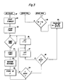
- Figure 3 through 5 are functional block diagrams of three embodiments of a method for testing analog devices according to the present invention.
- A schematic diagram of a test system 25 according to the present invention is illustrated in Figure 2, wherein the device 11, which is to be tested, i.e. typically one or more individual components within a printed circuit board, is brought into electrical contact with
probes 13 and thus with switchingmatrix 14.Such probes 13 and switchingmatrix 14 are of conventional design and need not be further explained to those skilled in the art. The parameters of the device 11 which are necessary to make a decision as to whether the device is functioning or not functioning are also programmed into the system 25. Such parameters would include not only the specific impedance, capacitance, or inductance values, or desired current and voltage levels, etc. for example, but also the acceptable tolerance ranges for the devices. Typically the configuration of the entire circuit board which is to be tested, including a description of the devices contained therein and their specific interconnections has been programmed into the system 25 such that theprobes 13 can be correctly positioned to contact specific test points, e.g. asnodes matrix 14 can be switched at the appropriate times to electrically connect thesignal generator 16 and themeasurement circuit 17 to the appropriate nodes, and such that appropriately shaped stimulus signals are generated. Thesignal generator 16 andmeasurement circuit 17 are also considered conventional in design and will not be further described herein.
Once this data is determined for a particular circuit board it is typically stored in a retrievable format such as on magnetic tape or disks which can be loaded into aconventional processor 15 in a conventional manner such as throughinput terminal 19, to initialize the parameters for the test, whenever that particular board is to be tested. - Upon instruction by the
processor 15, thesignal generator 16 provides the appropriate stimulus signal to theprobes 13 through thematrix 14. For example, a DC voltage of a predetermined magnitude can be applied atnode 20. Theprocessor 15 simultaneously sends a signal to to thetimer 18 that the stimulus signal has been applied, and instructs thematrix 14 to electrically connect themeasurement circuit 17 tonode probes 13. Since the switching circuits involved within thematrix 14 can introduce transient into the measurement circuit, theprocessor 15 typically waits a predetermined time before taking the first measurement, which time is a function of the particular switching circuits utilized. In the preferred embodiment this time is typically in the order of 1.5 milliseconds. After this initial wait time a first measurement is made atnode 21 of the response of device 11 to the input stimulus. Sincesuch measurement circuit 17 typically includes an amplifier, an RMS to DC converter, a DC scaling circuit, and an analog to digital converter, the measurement can be stored in a digital format. In the preferred embodiment this storage is done within standard memory units within theprocessor 15. - Before proceeding further it should be noted that the present invention as thus far described has been illustrated by block representations which show only those specific details that are pertinent to the present invention. This has been done so as not to obscure the disclosure with structured details which will be readily apparent to those skilled in the art having the benefit of the description herein. Accordingly, the block diagram illustrations may not necessarily represent the precise mechanical structural arrangement of an exemplary test system, but rather are primarily intended to depict the major components of such a system in a convenient functional grouping in light of which the present invention may be more readily understood.
- The relationship developed to predict the final value as part of the present invention has been empirically as well as theoretically derived and can be proven algebraically. It is based upon the assumptions that the input to the device is a basic first order step function, as well as the assumption that the measurement system has a dominant real pole such that it can be approximated as a first order system. This latter assumption is valid since compensation capacitors are typically utilized within the measurement circuitry. The resulting derived relationship is as follows:

- Where X,Y, and Z are samples taken at times T₁, T₂ and T₃ respectively.
This relationship requires three measurements to be taken with an equivalent time delay there between. The optimum time "T" between measurements is a function of the speed at which the response is changing, i.e. insignificant variance in the magnitude of the response signifies a response that has either substantially settled to its final value or a response being sampled too rapidly to measure any variance therein. Although a fast sampling rate is desirable to afford a rapid calculation of the predicted value, the time between measurements must be significantly large to afford a sufficiently large voltage or response variation to result in an acceptable signal to noise ratio for the predicted value calculation. A number of methods can be used to determine an optimum time "T", both apriori (through calculations based upon the parameters of the device being tested) or dynamically (based upon the actual variation in the response), to be utilized by the present invention. In the preferred embodiment a "T" is initially chosen which is known to be small in view of the parameters of the device 11 being tested. Measurements of the response are then made with this between-measurement interval being extended dynamically until the magnitude of the measured response equals approximately 12% of the expected final value, i.e. the derived value. The resulting "T" at which this value is achieved is utilized as the "T" between the measurements thereafter made and used to calculate the predicted final value. These calculations can be quickly made by thearithmetic processor 23 under the control of theprocessor 15. It should be apparent to those skilled in the art, however, that other methods for calculating a value for "T" may be equally viable. - To facilitate the timing accuracy of these measurements the present invention restarts the
timer 18 prior to taking each measurement. This eliminates any variation in the time between measurements due to a variation in the time taken for performing the measurement. In the simplest embodiment of the present invention all three measurements are made prior to any calculations for predicting the final value. Once taken, the three values are provided as inputs to a conventionalarithmetic processor 23 in which the predicted final value is calculated. - Once the final response or voltage is predicted, it is compared to the derived value for such response which has been previously stored in the
processor 15. Typically such comparison will have a range of tolerance over which a component will be found acceptable. This tolerance range has be programmed into theprocessor 15 during the initiation of the parameters as has already been described. Thus the device 11 under test will either be rejected or accepted. This status can be indicated by a message on the screen of a CRT, the generation of a printout, the lighting of indicators, etc. - The steps thus far described are illustrated in Figure 3. As can be seen
instruction 28 initializes theprocessor 15 with the testing parameters including the derived valued and the tolerance range for the device 11 under test.Instruction 29 causes the switchingmatrix 14 to electrically connect theappropriate probes 13 to thesignal generator 16, and also causes thesignal generator 16 to apply the appropriate stimulus signal to the nodes of the device 11. The application of the stimulus signal activates thetimer 18 as is indicated byinstruction 30.Instruction 30 also causes the switching matrix to connect the appropriate probes to themeasurement circuit 17. Since the accurate control of the elapsed time between measurements is critical,instruction 31 restarts the timer as soon as the programmed time delay has expired. A first measurement of the response of the device to the stimulus signal is then taken as a result ofinstruction 32. This measurement is identified as measurement "Z" and stored in theprocessor 15 byinstruction 33. If this is the first measurement,instruction 34 will respond with a "no" andinstruction 35 will cause the first measurement to also be stored as measurement "Y".
Upon expiration of the programmed time delay oftimer 18,instructions 31 through 34 will be repeated and the second measurement will be stored as measurement "Z". Since measurement "Y" now exists (i.e., the first measurement) control will pass toinstructions time delay instructions 31 through 34 and 36 are again repeated, only this time control passes toinstructions 38 since all three measurements now exist, I.E. X = first measurement, Y = second measurement, Z = third measurement. It can be seen by one skilled in the art that steps 33 through 37 function as a loop to ensure that the appropriate number of measurements are made. This result can also be achieved by other instruction sets which are considered to be equivalent to those described herein and thus within the scope of the present invention. -
Instruction 38 causes theprocessor 15 and thearithmetic processor 23 to process the measured values according to a mathematical relationship derived to predict the final value of the responses to the stimulus, i.e. the value which would occur at some time "Tf", which is greater than the settling time. Once this value is calculated it can be compared to the determined value which has been programmed into theprocessor 15 duringstep 28. As has already been stated, substantial equivalence (i.e. within the programmed tolerance range) between the predicted value and the determined value will lead to a conclusion that the device under test is functioning properly. - Although the simple embodiment thus far described is effective for testing a variety of circuits it is not totally satisfactory in all cases. Greater accuracy, for example, can be achieved by repeating this method and looking for a consistency between the final predicted values before comparing the predicted value to the determined value as illustrated by instructions 47-51 of Figure 4 (wherein instructions which are common to the embodiment illustrated in Figure 3 remain numbered as on Figure 3). This repetition is particularly useful for circuits having a large time constant, (i.e. a long settling time). If after multiple repetitions, the predicted final value remains relatively constant, there can be greater assurance that the method is indeed working with the particular circuit. Since the time delay between measurements is typically quite small compared to the total elapsed time for the response to each steady-state, the multiple repetitions of the method according to the present invention can still be performed in substantially less time than conventional test systems which wait for the response to fully settle.
- Similarly the accuracy and speed of the above method can be further increased by including some additional method steps as are shown in the embodiment illustrated in Figure 5 (wherein instructions which are common to the embodiment illustrated in Figure 3 remain numbered as in Figure 3). As can be seen,
instructions 28 through 35 remain identical. With this embodiment however, the existence of a second measurement will lead toinstruction 40 which compares the two most recent measurements. If such measurements are substantially equivalent, i.e. within a programmed tolerance range, an assumption can be made that the response has already reached a steady state or final value. Thusinstruction 39 can be applied to make the comparison between the measured response and the derived response to determine whether or not the device 11 is functioning properly, without processinginstruction 38. Accordingly both time and memory space can be saved. If however the measurements are not substantially equivalent,instruction 36 is processed. Depending upon whether a third measured value is currently in memory, eitherinstruction Instruction 37 leads into the measurement loop which has already been discussed.Instruction 41 however, determines the ratio of the difference between the first and second measured values to the difference between the second and third values. (The nomenclature third, second and first is used for convenience to indicate the most recent measurement, the prior measurement and the measurement before the prior measurement, respectively.) This ratio is then stored in theprocessor 15 as ratio "R". If only three measurements are in memory this ratio is also stored as ratio "S" and a fourth measurement is made in the conventional manner viainstructions instruction 41 is again processed and the ratio "R" is calculated and stored utilizing the second, third and fourth measurement. The ratio "S" however now exists due to the initial processing ofinstructions 41 and 42. Thusinstruction 43 is processed. Empirical investigations with the present inventions have determined that the test method according to the present invention is more efficient and potentially more accurate when the ratios as calculated byinstruction 41 are substantially equal. This premise has also been mathematically confirmed. Similarly greater accuracy is achieved when the ratios are positive and greater than unity.Instruction 44 makes this determination. If either of these conditions is not met, another measurement is made viainstruction arithmetic processor 23. This process is repeated until the conditions hold true. - In the preferred embodiment the occurrence of both of the conditions set forth by
instructions instruction 38 and a determination of the condition of the device viainstruction 39 as has already been described. Typically such a determination can be made within a fraction of the time required for the response to fully settle. The actual time taken is, however, dependent upon the time constant of circuit being tested. For most circuits the time taken to predict the final value is approximately one half of this time constant. - It can be seen that the present invention affords a determination of the condition of the device under test in substantially less time than conventional testing systems which are currently available. Furthermore such reduction in test time can be accomplished with minimal reduction in accuracy for most circuits.
- While we have shown and described multiple embodiments of the present invention it will be understood that the such invention is not limited thereto, but rather that changes and modifications may be made to the configuration or identity of some of the parts and/or the order or identity of some of the method steps described and as would be known to a person skilled in the art, without departing from the present invention as set forth in the appended claims.
Claims (10)
- A method for testing an analog device over a predetermined measurement interval characterized by(a) applying a pre-determined input signal to the device, said input signal being invariant over said measurement interval, said analog device having a response to said input signal which is a continuous function asymptotically approaching a final value,(b) taking a first measurement of the response of the device resulting from the input signal,(c) waiting a predetermined time T and taking a second measurement of the response of the device resulting from the input signal,(d) waiting the same predetermined time T as in step (c) and taking a third measurement of the response of the device resulting from the input signal,(e) predicting the final value of the response from the measured values alone without waiting to actually measure the final value, and(f) repeating steps (a) through (e) and comparing the predicted final values;(g) comparing the predicted final response to a known response value derived from a functioning device when the predicted final values compared in step (f) are substantially equivalent.
- A method according to Claim 1 characterized in that said function is a negative exponential function.
- A method according to Claim 2 characterized in that said negative exponential function is of the form of e-kt or 1-e-kt.
- A method according to any one of Claims 1-3 characterized in that said final value is predicted according to the following relationship:

X equals the first measured value,
Y equals the second measured value and
Z equals the third measured value. - A method according to any one of the preceeding claims characterized by comparing the second measurement to the first measurement, and stopping said method at step (c) if said first and second measurements do not differ by more than a predetermined value.
- A method according to any one of the Claims 1-4 characterized by comparing the difference between the first and second measurements to the difference between the second and third measurements, and stopping said method at step (d) if the ratio of the difference between the second and third measurements is not positive and greater than unity.
- A method according to any one of Claims 1-4 characterized in that step d) further comprises waiting the same predetermined time T as in step (c) taking a fourth measurement of the response of device resulting from the input signal, deriving a ratio of the difference between the first and second measurement to the difference between the second and third measurements, deriving a ratio of the difference between the second and third measurements to the difference between the third and fourth measurements, comparing the ratio of the difference between the first and second measurements to the difference between the second and third measurements to the ratio of the difference between the second and third measurements to the difference between the third and fourth measurements and performing step (e) only when such compared ratios are equal, positive and greater than 1.
- A system for testing an analog device over a measurement interval characterized by a signal generator for stimulating the device with a predetermined electrical signal, said electrical signal being invariant over said measurement interval,
means for taking at least three measurements of the response of the device to the stimulus signal, which measurements are separated by a predetermined and equal time delay,
circuit means for selectively electrically connecting and/or disconnecting said measurement means and said signal generator to the device,
means for predicting the final value of the response of the device to the stimulus signal from the measured values,
according to the following relationship:
X equals the first measured value of the response,
Y equals the second measured value of the response and
Z equals the third measured value of the response, and
means for comparing the predicted final response to a response value derived from a functioning device thereby evaluating whether the device under test is functioning or not functioning. - Apparatus of Claim 8 characterized by:
means for comparing the ratio of the difference between the first and second measurement to the difference between the second and third measurements; and in that said means for predicting the final value does not predict the final value when such ratio is not positive and greater than unity. - Apparatus of Claim 8 characterized by:
means for taking a fourth measurement of the response of the device to the stimulus signal, said measurement being separated by said predetermined and equal time delay,
means for comparing the ratio of difference between the first and second measurements to the difference between the second and third measurements;
means for comparing the ratio of the difference between the second and third measurements to the difference between the third and fourth measurements; and in that said means for predicting the final value does not predict the final value when such ratios are not equal, positive and greater than unity.
Applications Claiming Priority (2)
| Application Number | Priority Date | Filing Date | Title |
|---|---|---|---|
| US632460 | 1984-07-19 | ||
| US06/632,460 US4686628A (en) | 1984-07-19 | 1984-07-19 | Electric device or circuit testing method and apparatus |
Publications (2)
| Publication Number | Publication Date |
|---|---|
| EP0171322A1 EP0171322A1 (en) | 1986-02-12 |
| EP0171322B1 true EP0171322B1 (en) | 1991-09-11 |
Family
ID=24535614
Family Applications (1)
| Application Number | Title | Priority Date | Filing Date |
|---|---|---|---|
| EP85401474A Expired - Lifetime EP0171322B1 (en) | 1984-07-19 | 1985-07-18 | Electric device or circuit testing method and apparatus |
Country Status (5)
| Country | Link |
|---|---|
| US (1) | US4686628A (en) |
| EP (1) | EP0171322B1 (en) |
| JP (1) | JPH065261B2 (en) |
| CA (1) | CA1248181A (en) |
| DE (1) | DE3584054D1 (en) |
Families Citing this family (22)
| Publication number | Priority date | Publication date | Assignee | Title |
|---|---|---|---|---|
| EP0192981B1 (en) * | 1985-01-31 | 1989-12-27 | Hewlett-Packard Company | Circuit for measuring characteristics of a device under test |
| US5043910A (en) * | 1985-04-19 | 1991-08-27 | Graphtec Kabushikikaisha | Printed circuit board function testing system |
| DE3636427A1 (en) * | 1986-10-25 | 1988-05-05 | Standard Elektrik Lorenz Ag | CIRCUIT ARRANGEMENT AND MESSAGE NETWORK WITH TEST DEVICE AND TEST METHOD |
| US5107969A (en) * | 1987-09-17 | 1992-04-28 | Alfred Teves Gmbh | Controllable vibration damper |
| US5307290A (en) * | 1988-10-18 | 1994-04-26 | Fiat Auto S.P.A. | System for the automatic testing, preferably on a bench, of electronic control systems which are intended to be fitted in vehicles |
| US5134998A (en) * | 1990-04-26 | 1992-08-04 | Minnesota Mining And Manufacturing Company | System and method for predicting the value of a compositional parameter of blood |
| GB2307051B (en) * | 1995-11-06 | 1999-11-03 | Marconi Instruments Ltd | An equipment for testing electronic circuitry |
| FR2749396B1 (en) * | 1996-05-29 | 1998-08-07 | Softlink | HELP TOOL FOR ELECTRONIC COMPONENT TESTING APPARATUS |
| FR2796157B1 (en) * | 1999-07-05 | 2002-05-31 | Softlink | METHOD FOR TESTING ELECTRONIC COMPONENTS |
| FR2812401B1 (en) * | 2000-07-28 | 2002-10-11 | Bealach Bo No Finne Teo Ta Gal | METHOD FOR TESTING ELECTRONIC COMPONENTS TAKING ACCOUNT OF THE AVERAGE DERIVATIVE |
| JP2003130919A (en) * | 2001-10-25 | 2003-05-08 | Agilent Technologies Japan Ltd | Connection box, and dut board evaluation system and method |
| US6760680B2 (en) * | 2002-10-09 | 2004-07-06 | Nyt Press Services Llc | Testing system for printing press circuit board controllers |
| US7231573B2 (en) * | 2002-12-20 | 2007-06-12 | Verigy Pte. Ltd. | Delay management system |
| JP4777794B2 (en) * | 2006-02-14 | 2011-09-21 | 日置電機株式会社 | measuring device |
| JP4275696B2 (en) * | 2006-11-09 | 2009-06-10 | 三菱電機株式会社 | Sampling frequency control system and protective relay |
| TWM343792U (en) * | 2008-06-10 | 2008-11-01 | Princeton Technology Corp | Circuit testing apparatus |
| TWM343798U (en) * | 2008-06-25 | 2008-11-01 | Princeton Technology Corp | Circuit testing apparatus |
| US8527231B2 (en) * | 2010-09-15 | 2013-09-03 | Teradyne, Inc. | High throughput semiconductor device testing |
| US8549764B2 (en) | 2011-09-23 | 2013-10-08 | Lexmark International, Inc. | Fluid tilt sensor within ink tank supply item for micro-fluid applications |
| TW201412027A (en) * | 2012-09-14 | 2014-03-16 | Chicony Electronics Co Ltd | Matrix testing method and system and voltage clock control method |
| US10340919B2 (en) * | 2017-11-29 | 2019-07-02 | Taiwan Semiconductor Manufacturing Company Limited | Circuit for monitoring transient time in analog and digital systems |
| DE102018217406B4 (en) * | 2018-06-18 | 2020-07-23 | ATEip GmbH | Method and device for electrically testing an electrical assembly |
Citations (1)
| Publication number | Priority date | Publication date | Assignee | Title |
|---|---|---|---|---|
| US3978325A (en) * | 1973-09-05 | 1976-08-31 | Control Electronics Co., Inc. | Electronic thermometer |
Family Cites Families (6)
| Publication number | Priority date | Publication date | Assignee | Title |
|---|---|---|---|---|
| US3541441A (en) * | 1969-02-17 | 1970-11-17 | Ibm | Test system for evaluating amplitude and response characteristics of logic circuits |
| US4162531A (en) * | 1977-01-14 | 1979-07-24 | Hewlett-Packard Company | Method and apparatus for programmable and remote numeric control and calibration of electronic instrumentation |
| US4176556A (en) * | 1977-06-17 | 1979-12-04 | Omron Tateisi Electronics Co. | Electronic thermometer |
| JPS58700A (en) * | 1981-06-26 | 1983-01-05 | Hitachi Ltd | Control method for fluid transport system |
| US4455612A (en) * | 1982-01-27 | 1984-06-19 | Iowa State University Research Foundation, Inc. | Recursive estimation in digital distance relaying system |
| US4574359A (en) * | 1982-12-21 | 1986-03-04 | Terumo Kabushiki Kaisha | Electronic clinical thermometer, and method of measuring body temperature |
-
1984
- 1984-07-19 US US06/632,460 patent/US4686628A/en not_active Expired - Fee Related
-
1985
- 1985-07-18 CA CA000487002A patent/CA1248181A/en not_active Expired
- 1985-07-18 EP EP85401474A patent/EP0171322B1/en not_active Expired - Lifetime
- 1985-07-18 DE DE8585401474T patent/DE3584054D1/en not_active Expired - Fee Related
- 1985-07-19 JP JP60158509A patent/JPH065261B2/en not_active Expired - Lifetime
Patent Citations (1)
| Publication number | Priority date | Publication date | Assignee | Title |
|---|---|---|---|---|
| US3978325A (en) * | 1973-09-05 | 1976-08-31 | Control Electronics Co., Inc. | Electronic thermometer |
Also Published As
| Publication number | Publication date |
|---|---|
| US4686628A (en) | 1987-08-11 |
| JPH065261B2 (en) | 1994-01-19 |
| JPS6188170A (en) | 1986-05-06 |
| EP0171322A1 (en) | 1986-02-12 |
| DE3584054D1 (en) | 1991-10-17 |
| CA1248181A (en) | 1989-01-03 |
Similar Documents
| Publication | Publication Date | Title |
|---|---|---|
| US4686628A (en) | Electric device or circuit testing method and apparatus | |
| KR940701546A (en) | Method and device for charging and testing the battery | |
| JP3093285B2 (en) | Testing electronic components | |
| JPH04294286A (en) | Method for measuring breakdown voltage | |
| EP0439921A2 (en) | Apparatus and method of testing arbitrary waveforms | |
| US6469516B2 (en) | Method for inspecting capacitors | |
| US5568055A (en) | Adiabatic conductor analyzer method and system | |
| US3822398A (en) | Method and apparatus for testing resistivity of reed relay contacts | |
| CN110857953A (en) | Tester and method for measuring resistance of conductor connection point in power-on circuit | |
| JP2002228695A (en) | Resistance measuring device | |
| JP4259692B2 (en) | Circuit board inspection equipment | |
| US5936419A (en) | Test method and apparatus utilizing reactive charging currents to determine whether a test sample is properly connected | |
| RU2086053C1 (en) | Method for checking characteristics of storage battery | |
| JPH0785094B2 (en) | Voltage difference measuring method and measuring apparatus therefor | |
| JP3213910B2 (en) | Battery diagnostic device | |
| JPH09178820A (en) | Test device for electronic circuit | |
| JP2730504B2 (en) | Test probe pin contact failure judgment method and in-circuit tester | |
| JPS6195258A (en) | Apparatus for testing integrated circuit | |
| EP0076120A2 (en) | Current generating circuit device for measuring cryogenic liquefied gas liquid level meter with superconductive wire | |
| US20240264104A1 (en) | Test apparatus and method | |
| JPS6329277A (en) | Testing device for logic integrated circuit | |
| RU2079919C1 (en) | Starters and relays insulation strength test stand | |
| JPH06186279A (en) | Electric characteristic tester | |
| JP2001091553A (en) | Device for measuring insulation resistance in capacitive electronic parts | |
| JPS6188716A (en) | Inspection monitor system of digital protective relay |
Legal Events
| Date | Code | Title | Description |
|---|---|---|---|
| PUAI | Public reference made under article 153(3) epc to a published international application that has entered the european phase |
Free format text: ORIGINAL CODE: 0009012 |
|
| AK | Designated contracting states |
Designated state(s): DE FR GB IT NL |
|
| 17P | Request for examination filed |
Effective date: 19860730 |
|
| 17Q | First examination report despatched |
Effective date: 19880414 |
|
| RAP1 | Party data changed (applicant data changed or rights of an application transferred) |
Owner name: FAIRCHILD SEMICONDUCTOR CORPORATION |
|
| RAP1 | Party data changed (applicant data changed or rights of an application transferred) |
Owner name: SCHLUMBERGER TECHNOLOGIES, INC. |
|
| GRAA | (expected) grant |
Free format text: ORIGINAL CODE: 0009210 |
|
| AK | Designated contracting states |
Kind code of ref document: B1 Designated state(s): DE FR GB IT NL |
|
| PG25 | Lapsed in a contracting state [announced via postgrant information from national office to epo] |
Ref country code: IT Free format text: LAPSE BECAUSE OF FAILURE TO SUBMIT A TRANSLATION OF THE DESCRIPTION OR TO PAY THE FEE WITHIN THE PRESCRIBED TIME-LIMIT;WARNING: LAPSES OF ITALIAN PATENTS WITH EFFECTIVE DATE BEFORE 2007 MAY HAVE OCCURRED AT ANY TIME BEFORE 2007. THE CORRECT EFFECTIVE DATE MAY BE DIFFERENT FROM THE ONE RECORDED. Effective date: 19910911 |
|
| REF | Corresponds to: |
Ref document number: 3584054 Country of ref document: DE Date of ref document: 19911017 |
|
| ET | Fr: translation filed | ||
| PGFP | Annual fee paid to national office [announced via postgrant information from national office to epo] |
Ref country code: FR Payment date: 19920615 Year of fee payment: 8 |
|
| PLBE | No opposition filed within time limit |
Free format text: ORIGINAL CODE: 0009261 |
|
| STAA | Information on the status of an ep patent application or granted ep patent |
Free format text: STATUS: NO OPPOSITION FILED WITHIN TIME LIMIT |
|
| PGFP | Annual fee paid to national office [announced via postgrant information from national office to epo] |
Ref country code: NL Payment date: 19920731 Year of fee payment: 8 |
|
| 26N | No opposition filed | ||
| PGFP | Annual fee paid to national office [announced via postgrant information from national office to epo] |
Ref country code: GB Payment date: 19930621 Year of fee payment: 9 |
|
| PGFP | Annual fee paid to national office [announced via postgrant information from national office to epo] |
Ref country code: DE Payment date: 19930930 Year of fee payment: 9 |
|
| PG25 | Lapsed in a contracting state [announced via postgrant information from national office to epo] |
Ref country code: NL Effective date: 19940201 |
|
| NLV4 | Nl: lapsed or anulled due to non-payment of the annual fee | ||
| PG25 | Lapsed in a contracting state [announced via postgrant information from national office to epo] |
Ref country code: FR Effective date: 19940331 |
|
| REG | Reference to a national code |
Ref country code: FR Ref legal event code: ST |
|
| PG25 | Lapsed in a contracting state [announced via postgrant information from national office to epo] |
Ref country code: GB Effective date: 19940718 |
|
| GBPC | Gb: european patent ceased through non-payment of renewal fee |
Effective date: 19940718 |
|
| PG25 | Lapsed in a contracting state [announced via postgrant information from national office to epo] |
Ref country code: DE Effective date: 19950401 |