EP0168166B1 - Gleichstromversorgungsschaltung - Google Patents
Gleichstromversorgungsschaltung Download PDFInfo
- Publication number
- EP0168166B1 EP0168166B1 EP85304036A EP85304036A EP0168166B1 EP 0168166 B1 EP0168166 B1 EP 0168166B1 EP 85304036 A EP85304036 A EP 85304036A EP 85304036 A EP85304036 A EP 85304036A EP 0168166 B1 EP0168166 B1 EP 0168166B1
- Authority
- EP
- European Patent Office
- Prior art keywords
- voltage
- resistor
- power supply
- building
- current
- Prior art date
- Legal status (The legal status is an assumption and is not a legal conclusion. Google has not performed a legal analysis and makes no representation as to the accuracy of the status listed.)
- Expired
Links
Images
Classifications
-
- H—ELECTRICITY
- H02—GENERATION; CONVERSION OR DISTRIBUTION OF ELECTRIC POWER
- H02M—APPARATUS FOR CONVERSION BETWEEN AC AND AC, BETWEEN AC AND DC, OR BETWEEN DC AND DC, AND FOR USE WITH MAINS OR SIMILAR POWER SUPPLY SYSTEMS; CONVERSION OF DC OR AC INPUT POWER INTO SURGE OUTPUT POWER; CONTROL OR REGULATION THEREOF
- H02M3/00—Conversion of DC power input into DC power output
- H02M3/22—Conversion of DC power input into DC power output with intermediate conversion into AC
- H02M3/24—Conversion of DC power input into DC power output with intermediate conversion into AC by static converters
- H02M3/28—Conversion of DC power input into DC power output with intermediate conversion into AC by static converters using discharge tubes with control electrode or semiconductor devices with control electrode to produce the intermediate AC
- H02M3/325—Conversion of DC power input into DC power output with intermediate conversion into AC by static converters using discharge tubes with control electrode or semiconductor devices with control electrode to produce the intermediate AC using devices of a triode or a transistor type requiring continuous application of a control signal
- H02M3/335—Conversion of DC power input into DC power output with intermediate conversion into AC by static converters using discharge tubes with control electrode or semiconductor devices with control electrode to produce the intermediate AC using devices of a triode or a transistor type requiring continuous application of a control signal using semiconductor devices only
- H02M3/33507—Conversion of DC power input into DC power output with intermediate conversion into AC by static converters using discharge tubes with control electrode or semiconductor devices with control electrode to produce the intermediate AC using devices of a triode or a transistor type requiring continuous application of a control signal using semiconductor devices only with automatic control of the output voltage or current, e.g. flyback converters
- H02M3/33523—Conversion of DC power input into DC power output with intermediate conversion into AC by static converters using discharge tubes with control electrode or semiconductor devices with control electrode to produce the intermediate AC using devices of a triode or a transistor type requiring continuous application of a control signal using semiconductor devices only with automatic control of the output voltage or current, e.g. flyback converters with galvanic isolation between input and output of both the power stage and the feedback loop
Definitions
- the present invention relates to power supplies and more particularly, to a power supply for producing a precise constant output irrespective of variations in the AC input voltage provided thereto and irrespective of changes in the load.
- a number of power supply arrangements are presently commercially available to provide a precise output irrespective of the variations in AC input voltage and changes in the load.
- one type of power supply is a switching device for selectively turning on and off the input voltage.
- the input voltage is provided to rectifying and filtering networks which develop the desired output voltages.
- a feedback control loop samples the output of the power supply and provides the sampled voltage output to a comparison circuit which comprises the sampled output with a reference voltage.
- a control signal is developed by the comparison circuit which is used to operate the switching device to switch on and off the input voltage at a rate to make the output voltage constant.
- WO 85/00939 which is prior art within the terms of Art 54(3) EPC discloses a DC power supply in which the output voltage is compared with a reference voltage and a resulting voltage controls the duty cycle of the oscillator coupled to the primary windings of the device.
- prior art power supplies have disadvantages in that generally it is more difficult to sample voltage output as voltage and make comparison thereof than to sample voltage outputs as current and make comparison thereof. Further such prior art devices provide no compensating signal to the reference source to compensate for the error signal. Also there is generally no consideration given to synchronizing the timing of switching on the input voltage at the same point in the cycle thereof in order to provide a precise voltage output.
- the present invention is directed to overcoming the disadvantages of the prior art.
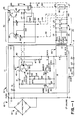
- Power Supply 10 includes the following subcomponents: high voltage input circuit 11 comprising AC power input circuitry 12 and charge buildup and transfer circuitry 14, triggering circuit 16 including opto-coupler 18, output filter and load circuitry 20, and sensing circuit 22 including protection circuit 24.
- the individual components are identified and valued as follows:
- the high voltage input circuit 11 includes a full wave rectifier bridge 30 which includes four diodes such as diode 32.
- the rectifier bridge 30 rectifies a 120V AC line.
- Rectifier 30 is provided in parallel with a capacitor C 1 .
- Capacitor C 1 becomes a DC source of unregulated voltage V c1 (about 150 volts DC).
- the high voltage input circuit 11 further includes a transformer coil L 1 which is connected in series with capacitor C 1 and which communicates through a thyristor SCR 3 to the main charging capacitor C 4 .
- the other terminal of C 4 is connected to the ground end of capacitor C 1 .
- the charge buildup and transfer circuit 14 include capacitor C 4 and transformer coil L 2 which define a tank circuit 34 that transfers power to transformer coils L 3 and L 4 as will be explained below.
- Capacitor C 4 starts discharging through transformer coil L 2 .
- capacitor C 4 starts discharging through transformer coil L 2 even during the charging of capacitor C 4 , but because transformer coil L 2 is much larger than transformer coil L 1 , the current through coil L 2 is smaller, therefore allowing the voltage V c4 of capacitor C 4 to remain higher than V c1 across capacitor C 1 for a long enough period to allow thyristor SCR 3 to turn off.
- diode D 5 will conduct current to the filtering and load circuits 20.
- the tank circuit 34 can continue to oscillate, transferring decreasing amounts of energy alternatively through diodes D 5 and D 6 .
- the currents through diodes D 5 and D 6 and the voltage across coils L 3 and L 4 are averaged out by the inductors L 5 and L 6 and capacitors C 7 , C 8 and C 9 which comprise the output filter 36 of filter and load circuitry 20.
- snubbers comprised of resistor R 1 and capacitor C 2 , and also resistor R 14 and capacitor C 5 , and also resistor R 15 and capacitor C 6 .
- the triggering circuit 16 is provided in order to trigger the charging of capacitor C 4 by coil L 1 to maintain a constant voltage across the load.
- the trigger circuit 16 receives an input from the sensing circuit 22 which is proportional to the difference between the desired reference voltage V ref and the voltage provided to the load as measured by a current comparison.
- This input is in the form of a current which is directly proportional to the size of the voltage difference which is provided to the light emitting diode 40 of opto-coupler 18. This current controls the timing of the triggering of thyristor SCR 3 .
- the basic elements of the triggering circuit include opto-coupler 18, unijunction transistor UJT 2 , capacitor C 3 , Zener diode Z 3 , diode D 2 , thyristor SCR 3 and resistors R 7 , R 8 and R 9 .
- Opto-coupler 18, resistor R 7 and diode D 2 provide communication between capacitor C 1 and base 2 of transistor UJT 2 .
- Base 1 of transistor UJT 2 is communicated to the gate G of thyristor SCR 3 through resistor R 8 and with ground through resistors R 8 and R 9 and capacitor C 4 .
- the series combination of resistor R 5 and capacitor C 3 is provided in a parallel arrangement with Zener diode Z 3 . This parallel arrangement is communicated between capacitor C 1 with other elements such as thyristor SCR 1 and resistors R 3 , R 4 which will be discussed below, and ground.
- Transistor UJT 2 is constructed such that when the voltage applied to emitter E 2 rises to a certain ratio (intrinsic ratio) of the voltage applied to base 2, the resistance between emitter and base 1 of transistor UJT 2 become very small, allowing capacitor C 3 to discharge across transistor UJT 2 .
- capacitor C 4 Assume the voltage across capacitor C 4 (V C4 ) is higher than the voltage across the series combination of coil L 1 and C 1 (V L1 ), the voltage across the triggering circuit 16 is essentially zero because diode D 2 is reverse biased, and capacitor C 3 is completely discharged.
- capacitor C 4 communicates with diode D 2 through zener diodes Z 1 , Z 2 , Z 3 and resistor R 7 .
- V C4 decreases with respect to V L1 , eventually diode D 2 is forward biased, and current starts charging up capacitor C 3 and immediately sets the voltage across Zener diode Z 3 to a maximum voltage V z3 . Given sufficient time, the voltage across C 3 (V C3 ) will rise to V Z3 .
- the object of regulation is to maintain a constant voltage V L across the load 38.
- V L voltage across the load 38.
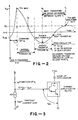
- a single control modulates both frequency and charged voltage V c4 . Since both frequency and voltage are controlled, the frequency need not change very much from full load to almost zero load. In fact the frequency need only change from about 30 KHz to 15 KHz.
- the maximum charged voltage of capacitor C 4 , V c4max depends on where the triggering occurs. If V c4t is the algebraic value of V c4 at triggering time, then:
- the energy transferred per cycle is thus:
- the time T s where the charging of capacitor C 3 of the triggering circuit 16 begins is always synchronized with the V c4 waveform because V C3 remains zero from the last triggering up to T s (where V c4 begins to be lower than V c1 ).
- the charging of C 3 also follows a fixed pattern in time because resistor R 5 and capacitor C 3 and the voltage V Z3 at Zener diode Z 3 are constants during this charging.
- the timing for the next triggering is done by varying the base 2 voltage of transistor UJT 2 which depends on how much current is fed to it from transistor 42 of opto-coupler 18.
- the amount of current flowing through the diode 40 of the opto-coupler 18 comes from the sensing circuit 22 (discussed below).
- the rate of charging of capacitor C 3 is a constant and the voltage at base 2 of transistor UJT 2 is varied with time, depending on the signal from the sensing circuit 22.
- a diode D 1 is used to assure that V base2 of transistor UJT 2 never goes below V z3 where improper triggering of transistor SCR 3 may occur (i.e., insufficient voltage to turn on transistor SCR 3 ).
- series resistors R 3 and R 4 are provided in parallel with thyristor SCR 1 , with the gate of thyristor SCR 1 communicating with the interconnection between resistors R 3 and R 4 .
- This parallel arrangement between resistors R 3 , R 4 and thyristor SCR 1 communicates capacitor C 1 with resistor R 5 and capacitor C 3 via diode D 2 , resistor R 7 and Zener diodes Z 1 , Z 2 .
- resistor R 3 In start-up there must be a large resistor R 3 in series with resistor R 5 to slow down the charging of capacitor C 3 , allowing time for the voltage at the base B 2 of the transistor UJT 2 to grow large enough for the triggering of thyristor SCR 3 . But resistor R 3 must drop out during normal operation. This is achieved with transistor SCR 1 .
- the thyristor SCR 1 After the first discharge, the thyristor SCR 1 will be turned on at the next charging of capacitor C 3 because the current through resistor R 3 is then large enough to turn on thyristor SCR 1 , thus bypassing resistor R 3 . Since the turn-off time of thyristor SCR 1 is chosen to be large, SCR 1 is essentially on all the time after the first shooting of capacitor C 3 .
- a unijunction transistor UJT 1 is also provided with base 2 thereof communicating with the series interconnection between Zener diode Z 1 and Z 2 and base 1 connecting with resistor R 2 .
- the emitter E 1 of transistor UJT 1 communicates with the series interconnection between resistors R 5 and capacitor C 3 and thus with the emitter E 2 of transistor UJT 2 .
- thyristor SCR 3 may not turn off when it is triggered at V c4 too close to V c1 ( Figure 2). Therefore capacitor C 3 has to be discharged by some means when the voltage V base2 of transistor UJT 2 imposes a triggering time where V c4t is too close to V c1 (around V c4med in Figure 2).
- resistor R 7 is chosen such that thyristor SCR 3 cannot be turn-on when V c4t is near V c1 .
- the current through resistor R 7 is primarily channelled into the transistor UJT 2 because V Z1 +V Z2 +V Z3 is higher than the base 2 voltage of UJT 2 (the impedances of the Zener diodes Z 1 , Z 2 and Z 3 are at this point very large).
- Resistor R 7 allows only enough current to maintain V base2 of transistor UJT 2 high, preventing the discharge of capacitor C 3 to thyristor SCR 3 .
- the V base2 of transistor UJT 1 is deprived of current and fully conducts as the emitter voltage is greater than the intrinsic ratio times the voltage at base 2, discharging capacitor C 3 into resistor R 2 .
- thyristor SCR 3 over current protection for thyristor SCR 3 is provided by thyristor SCR 2 and resistors R 10, R 11, R 12, R, 3 and diodes D 3 , D 4 .
- resistors R 12 , R 13 are provided in tank circuit 34 with thyristor SCR 2 and resistor R 10, R 4 and diodes D 3 , D 4 connected between tank circuit 34 and capacitor C 1 .
- the sensing circuit 22 provides a current to opto-coupler 18 that is proportional to the difference between the desired or reference voltage V ref across the load and the actual voltage across the load V L as measured by a current comparison discussed below.
- the sensing circuit 22 is principally comprised of resistors R 16 , R 17, R 18 and R 19, transistor or NFET 26 and a current amplification device T 1 comprised of transistor pair 28.
- Resistor R 16 is provided in communication with the load 38 so as to sense the current through load 38 returning to the power supply 10.
- Potentiometer or Resistor R 18 is provided in parallel with resistor 16 and thus sees the same voltage as does resistor R 16 .
- the gate of transistor NFET 26 is connected to resistor R 18 with the drain connected to potentiometer or resistor R 17 which is connected to one end of resistor R 18.
- the source of transistor NFET 26 is connected to potentiometer or resistor R 19 and the base of the first transistor 44 in current amplification device T 1 .
- the other terminal of resistor R 19 communicates with the positive terminal to which the load 38 is connected.
- Device T 1 is comprised of two transistors 44, 46, the collectors of which communicate with the diode 40 of opto-coupler 18, and the emitter of the first transistor 44 communicates with the base of the second transistor 46.
- the emitter of the second transistor 46 communicates with the negative terminal (ground) to which the load 38 is connected.
- V BE of current amplification device T 1 can be considered constant, then: a linear function of V L .
- the current through the diode 40 of the opto-coupler 18 is roughly proportional to the deviation of V L from V reference .
- the signal from diode 40 creates a current through the transistor 42 of the opto-coupler 18 that is roughly proportional to ⁇ i.
- This current is fed to the interbase resistance (through base 2) of transistor UJT 2 , creating an almost proportional V base2 of transistor UJT2.
- This V base2 determines when the next triggering of thyristor SCR 3 and will occur as explained above.
- resistor R 18 is a potentiometer that biases the right amount of voltage from R 16 to the gate of transistor NFET 26 to exactly offset the ⁇ i used for regulation. The ⁇ i is still there, but it is on top of a higher reference i out such that the resulting V L remains unchanged and thus is not load dependent as this load changes.
- sensing circuit 22 includes diodes D 7 , D s , D 9 and D 10 along with resistors R 20 and R 21 . These components protect the power supply, should the user improperly connect lines 50 and 52.
- the sensing lines 50, 52 connecting diode D 9 and resistor R 19 to the load 38 cannot be permanently connected. Therefore user mistakes may occur, such as: (a) the user may forget to connect them to the load, or (b) the connections may be loose, or (c) the connecting lines may be broken, or (d) the connections may be to the wrong polarities. In these cases the power supply and the load must be protected from overvoltage because the power supply may run at maximum power if the sensing circuit is not connected properly.
- R 20 , R 21 , D 7 , D s , D 9 and D 10 are protected by R 20 , R 21 , D 7 , D s , D 9 and D 10 as follows.
- the sensing circuit 22 will sense the output voltage at capacitor C 9 instead, through resistor R 20 , which is connected to capacitor C 9 by line 54. The regulation is then for V c9 .
- V L is not held constant at V reference but at approximately V reference +V Fdiode .
- diode D 9 will block or isolate the positive line 52, and diode D 10 will return the current through the diode 40 of the opto-coupler 18 to the negative line 50. Since this current is now fairly large, the output power will be very small, depressing V L to a low voltage.
- Diode D 9 serves an additional purpose. That is, for increasing the source voltage of transistor NFET 26 so that it can operate properly. To maintain diode D 9 at a constant voltage drop, resistor R 21 is used to feed a large current through it.
- potentiometer R 17 is used for the adjusting of V L (and thus also i out ) in the range of from 4 volts to 8 volts.
- power source 10 can be made programmable to provide a programmable voltage output by replacing the constant current sink by a programmable current sink.
- the power supply can additionally be made to have a constant current output by replacing resistor R 19 by a constant current source such as a field effect transistor.
- low voltage rated SCRs can be used for higher input voltage if the voltage is divided and several charge buildup and transfer circuits, such as circuit 14, are provided in parallel across each portion of the divided input.
- the operation of the power supply 10 of the invention is as follows.
- a fully rectified voltage signal is provided to transformer coil L 1 .
- the voltage thereacross is transferred to capacitor C 4 of tank circuit 34 when thyristor SCR 3 is turned on by the trigger circuit 16.
- the charge is built up across capacitor C 4 , and that power is transferred through transformer coil L 2 to transformer coils L 3 and L 4 and therefrom to load 38.
- Sensing circuit 22 senses the output to the load 38 and provides a signal through opto-coupler 18 to the trigger circuit 16 in order to control the timing of the opening of thyristor SCR 3 .
Landscapes
- Engineering & Computer Science (AREA)
- Power Engineering (AREA)
- Electronic Switches (AREA)
- Control Of Electrical Variables (AREA)
- Power Conversion In General (AREA)
Claims (18)
Applications Claiming Priority (2)
| Application Number | Priority Date | Filing Date | Title |
|---|---|---|---|
| US06/618,219 US4646220A (en) | 1984-06-07 | 1984-06-07 | DC power supply with compensated current reference |
| US618219 | 1984-06-07 |
Publications (2)
| Publication Number | Publication Date |
|---|---|
| EP0168166A1 EP0168166A1 (de) | 1986-01-15 |
| EP0168166B1 true EP0168166B1 (de) | 1989-10-11 |
Family
ID=24476809
Family Applications (1)
| Application Number | Title | Priority Date | Filing Date |
|---|---|---|---|
| EP85304036A Expired EP0168166B1 (de) | 1984-06-07 | 1985-06-06 | Gleichstromversorgungsschaltung |
Country Status (4)
| Country | Link |
|---|---|
| US (1) | US4646220A (de) |
| EP (1) | EP0168166B1 (de) |
| JP (1) | JPS6134616A (de) |
| DE (1) | DE3573692D1 (de) |
Families Citing this family (3)
| Publication number | Priority date | Publication date | Assignee | Title |
|---|---|---|---|---|
| US4926280A (en) * | 1989-11-06 | 1990-05-15 | Ncr Corporation | Capacitor protection circuit for protecting storage capacitors in an electronic power supply |
| US5635869A (en) * | 1995-09-29 | 1997-06-03 | International Business Machines Corporation | Current reference circuit |
| US7738271B1 (en) | 2007-06-08 | 2010-06-15 | Science Applications International Corporation | Controlled resonant charge transfer device |
Family Cites Families (16)
| Publication number | Priority date | Publication date | Assignee | Title |
|---|---|---|---|---|
| US3197691A (en) * | 1962-01-02 | 1965-07-27 | Gen Electric | Regulated power supply |
| US3307098A (en) * | 1963-07-12 | 1967-02-28 | Jefferson Electric Co | Inverter having a single selfcommutating thyristor |
| US3414798A (en) * | 1966-09-01 | 1968-12-03 | Anchor Coupling Co Inc | Constant voltage power supply utilizing independent reference and control circuits coupled to each other by an optical link |
| NL6708900A (de) * | 1967-06-27 | 1967-09-25 | ||
| SE377988B (de) * | 1968-10-16 | 1975-08-04 | P E K Udden | |
| US3805142A (en) * | 1973-01-10 | 1974-04-16 | Bell Telephone Labor Inc | Current limit circuit with superseding characteristic to activate overcurrent protection circuit |
| US4055791A (en) * | 1975-09-08 | 1977-10-25 | Hewlett-Packard Company | Self commutated SCR power supply |
| US4069449A (en) * | 1976-02-03 | 1978-01-17 | Hughes Aircraft Company | Flyback type power supply |
| US4323959A (en) * | 1978-05-10 | 1982-04-06 | Hewlett-Packard Company | Power supply with resonant inverter circuit using variable frequency control for regulation |
| US4250541A (en) * | 1979-12-07 | 1981-02-10 | Rca Corporation | Push-push resonant power inverter |
| US4333133A (en) * | 1980-09-22 | 1982-06-01 | International Telephone And Telegraph Corporation | Power source with an electronic impedance changer |
| SU936279A1 (ru) * | 1980-10-07 | 1982-06-15 | Ленинградский Электротехнический Институт Связи Им.Проф.М.А.Бонч-Бруевича | Стабилизированный преобразователь посто нного напр жени в посто нное |
| FR2497038A1 (fr) * | 1980-12-19 | 1982-06-25 | Frager Jean | Generateur de courant asservi en puissance, notamment pour processus de decharge dans une atmosphere rarefiee |
| JPS57129177A (en) * | 1981-02-04 | 1982-08-11 | Toshiba Electric Equip Corp | Transistor inverter |
| JPS5958921A (ja) * | 1982-09-28 | 1984-04-04 | Murata Mfg Co Ltd | 安定化電源回路 |
| GB8321520D0 (en) * | 1983-08-10 | 1983-09-14 | Ritchie G S | Electrical power supply apparatus |
-
1984
- 1984-06-07 US US06/618,219 patent/US4646220A/en not_active Expired - Fee Related
-
1985
- 1985-06-06 DE DE8585304036T patent/DE3573692D1/de not_active Expired
- 1985-06-06 EP EP85304036A patent/EP0168166B1/de not_active Expired
- 1985-06-06 JP JP12163285A patent/JPS6134616A/ja active Pending
Also Published As
| Publication number | Publication date |
|---|---|
| EP0168166A1 (de) | 1986-01-15 |
| DE3573692D1 (en) | 1989-11-16 |
| US4646220A (en) | 1987-02-24 |
| JPS6134616A (ja) | 1986-02-18 |
Similar Documents
| Publication | Publication Date | Title |
|---|---|---|
| US4669036A (en) | d.c. to d.c. converter power supply with dual regulated outputs | |
| EP0123030B1 (de) | Schaltnetzteil mit isolierter Rückkopplung | |
| US5119013A (en) | Switching regulator with multiple isolated outputs | |
| US4471418A (en) | Switching power supply | |
| EP0384680B1 (de) | Kommutierende Schaltung | |
| US4948987A (en) | Secondary electric power source produced by current flow through a primary a.c. power circuit | |
| US4713740A (en) | Switch-mode power supply | |
| US4464585A (en) | Gate circuit of gate turn-off thyristor | |
| JPH07241075A (ja) | 電力変換における電流検出装置及び方法 | |
| US4626982A (en) | Series connected switching power supply circuit | |
| EP0168166B1 (de) | Gleichstromversorgungsschaltung | |
| US5095416A (en) | Push-pull converter current limiter | |
| US5036450A (en) | Spike limiting circuit | |
| JPS62155739A (ja) | 電源回路 | |
| US4213082A (en) | Voltage regulator | |
| US3987354A (en) | Regulating circuit | |
| US4922399A (en) | DC-to-DC converter having improved power supply arrangement | |
| EP0255330A2 (de) | System mit langsamem Anlauf für eine Steuerschaltung | |
| US5708572A (en) | Switched-mode power supply | |
| EP0247407B1 (de) | Leistungsversorgung der Schaltungsart | |
| AU599579B2 (en) | Dc chopped power supply from an ac voltage | |
| US4173039A (en) | Current based power supply | |
| SE511444C2 (sv) | Förfarande för begränsning av utströmmen ur switchat kraftaggregat av flyback-typ i överbelastningssituationer och switchat kraftaggregat av flyback-typ | |
| US4639662A (en) | Thyristor circuit for current regulation | |
| JP3447975B2 (ja) | スイッチング電源回路 |
Legal Events
| Date | Code | Title | Description |
|---|---|---|---|
| PUAI | Public reference made under article 153(3) epc to a published international application that has entered the european phase |
Free format text: ORIGINAL CODE: 0009012 |
|
| AK | Designated contracting states |
Designated state(s): DE FR GB |
|
| 17P | Request for examination filed |
Effective date: 19860613 |
|
| 17Q | First examination report despatched |
Effective date: 19871211 |
|
| GRAA | (expected) grant |
Free format text: ORIGINAL CODE: 0009210 |
|
| AK | Designated contracting states |
Kind code of ref document: B1 Designated state(s): DE FR GB |
|
| REF | Corresponds to: |
Ref document number: 3573692 Country of ref document: DE Date of ref document: 19891116 |
|
| ET | Fr: translation filed | ||
| PLBE | No opposition filed within time limit |
Free format text: ORIGINAL CODE: 0009261 |
|
| STAA | Information on the status of an ep patent application or granted ep patent |
Free format text: STATUS: NO OPPOSITION FILED WITHIN TIME LIMIT |
|
| 26N | No opposition filed | ||
| PGFP | Annual fee paid to national office [announced via postgrant information from national office to epo] |
Ref country code: GB Payment date: 19920323 Year of fee payment: 8 |
|
| PGFP | Annual fee paid to national office [announced via postgrant information from national office to epo] |
Ref country code: FR Payment date: 19920606 Year of fee payment: 8 |
|
| PGFP | Annual fee paid to national office [announced via postgrant information from national office to epo] |
Ref country code: DE Payment date: 19920629 Year of fee payment: 8 |
|
| PG25 | Lapsed in a contracting state [announced via postgrant information from national office to epo] |
Ref country code: GB Effective date: 19930606 |
|
| GBPC | Gb: european patent ceased through non-payment of renewal fee |
Effective date: 19930606 |
|
| PG25 | Lapsed in a contracting state [announced via postgrant information from national office to epo] |
Ref country code: FR Effective date: 19940228 |
|
| PG25 | Lapsed in a contracting state [announced via postgrant information from national office to epo] |
Ref country code: DE Effective date: 19940301 |
|
| REG | Reference to a national code |
Ref country code: FR Ref legal event code: ST |