EP0166358B1 - Network junction control device of an electric circuit - Google Patents
Network junction control device of an electric circuit Download PDFInfo
- Publication number
- EP0166358B1 EP0166358B1 EP85107505A EP85107505A EP0166358B1 EP 0166358 B1 EP0166358 B1 EP 0166358B1 EP 85107505 A EP85107505 A EP 85107505A EP 85107505 A EP85107505 A EP 85107505A EP 0166358 B1 EP0166358 B1 EP 0166358B1
- Authority
- EP
- European Patent Office
- Prior art keywords
- flip
- capacitor
- flop
- resistor
- switch
- Prior art date
- Legal status (The legal status is an assumption and is not a legal conclusion. Google has not performed a legal analysis and makes no representation as to the accuracy of the status listed.)
- Expired
Links
Images
Classifications
-
- H—ELECTRICITY
- H01—ELECTRIC ELEMENTS
- H01H—ELECTRIC SWITCHES; RELAYS; SELECTORS; EMERGENCY PROTECTIVE DEVICES
- H01H47/00—Circuit arrangements not adapted to a particular application of the relay and designed to obtain desired operating characteristics or to provide energising current
- H01H47/02—Circuit arrangements not adapted to a particular application of the relay and designed to obtain desired operating characteristics or to provide energising current for modifying the operation of the relay
- H01H47/18—Circuit arrangements not adapted to a particular application of the relay and designed to obtain desired operating characteristics or to provide energising current for modifying the operation of the relay for introducing delay in the operation of the relay
-
- H—ELECTRICITY
- H05—ELECTRIC TECHNIQUES NOT OTHERWISE PROVIDED FOR
- H05B—ELECTRIC HEATING; ELECTRIC LIGHT SOURCES NOT OTHERWISE PROVIDED FOR; CIRCUIT ARRANGEMENTS FOR ELECTRIC LIGHT SOURCES, IN GENERAL
- H05B47/00—Circuit arrangements for operating light sources in general, i.e. where the type of light source is not relevant
- H05B47/10—Controlling the light source
Definitions
- the influence of the device on the supply circuit varies according to the operating conditions of the device itself.
- the inductance is high only when the lamp is on. Consequently, as long as the lamp is not lit, the reactive power due to the capacitor is not compensated and this results in disturbances on the network as long as the discharge lamp is connected to the network without being switched on.
- a discharge lamp can only light up when the gases it contains have cooled down.
- the lamps go out and can only re-light after a certain time during which the capacitors create a disturbance on the network.
- a short cut leading to the extinction of the lamps subsequently causes a very significant disturbance which must be compensated by a increase in the power supplied to the network, failing which the reactive power of the capacitors is not compensated and the discharge lamps cannot be re-ignited.
- a device for controlling an electrical circuit characterized in that it comprises a first controlled switch open at rest, mounted on the electrical circuit, a second controlled switch, closed at rest, mounted in parallel with the first controlled switch, supply means of the control device connected to the electrical circuit upstream of the first and second controlled switches, first time-delay control means connected to the first controlled switch, second means of timing control connected to the second controlled switch and memory means connected to the second controlled switch, the timing of the first control means being at most equal to the timing of the second control means.
- the timing means comprise a resistor, one terminal of which is connected to the supply means and the other terminal of which is connected on the one hand to the input of the first flip-flop corresponding and on the other hand to a first terminal of a capacitor
- the holding means comprise a second flip-flop whose input is connected to the output of the first flip-flop and whose output is connected to a second terminal of the capacitor opposite to the first one.
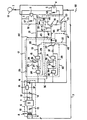
- the control device of an electrical circuit 1 comprises a first switch 2, open at rest,. controlled by a coil 3 and mounted on the electrical circuit 1, a second switch 4 closed at rest, mounted in parallel with the first switch 2 and controlled by a coil 5.
- the timing means 23 also include a capacitor 27 one of the terminals of which is also connected to line 26, while the other terminal is connected to ground through the inter medium of means for holding the control means in an activated position.
- These holding means are formed by a second flip-flop 28, one of the inputs of which is connected directly to ground and the other input of which is connected by a line 29 to the output of the first flip-flop 18, the output of the flip-flop 28 being connected to the terminal of the capacitor 27 which is opposite to the terminal of this same capacitor connected to the input of the rocker 18.
- Second timing control means comprise, in the same way as the first timing means 17, a flip-flop 31, connected via a resistor 32 to an NPN transistor 33.
- Timing means 34 comprise a resistor 35, one of which terminals is connected to the supply means 6 by a line 36 and the other terminal of which is connected to the input of the rocker 31.
- the timing means 34 also comprise a capacitor 37, a first terminal of which is connected to the input of the flip-flop 31 and the opposite terminal of which is connected to the output of a flip-flop 38 forming means for holding the control means 30 in an activated position.
- the flip-flop 38 has one of its input terminals connected to ground and the other input terminal connected to the output of the first flip-flop 31 by a line 39.
- the emitter of transistor 33 is connected to ground by a line 40 and the collector is connected to memory means 41, by means of a decoupling diode 42.
- the memory means 41 include a capacitor 43, one of which terminals is connected to the supply means 6 by a line 44 and is associated with a resistor 46, mounted in parallel with the terminals of the capacitor, by means of a resistor 45.
- the memory means 41 further comprise a second resistor 47, mounted in parallel with the first resistor 46 and in series with a switch 48, open at rest and controlled by a coil 49, one terminal of which is connected to the supply means 6 by a line 50 and the other bounded of which is grounded.
- the signal of the memory means is amplified by a PNP transistor 51, the base of which is connected to one of the common terminals of the resistors 46 and 47, the emitter of which is connected to the supply means 6 by a line 52 and of which the collector is connected to the base of an NPN transistor 53, via a resistor 54.
- the collector of transistor 53 is connected to the terminal of the coil 5 opposite to that which is connected to the supply means 6
- the emitter of transistor 53 is connected to ground by a line 55 and its base is also connected to ground via a resistor 56.
- Diodes 57, 58 and 59 are respectively mounted in parallel with the coils 3, 5 and 49 in order to protect the transistors against self-induction of these coils, during the interruption of the current therein.
- the operation of the device is as follows when establishing the connection with the AC voltage source 60, the switch 4 is closed and the current can flow normally towards the use, for example, a discharge lamp 61 which is cold and then lights up instantly.
- the flip-flop 18 is at rest and the transistor 20 is therefore blocked.
- the coil 3 is therefore not energized and the switch 2 is open.
- the coils 3 and 5 cease to be excited and the switches 2 and 4 return to their rest position.
- the capacitors 27 and 37 discharge almost instantaneously and the rockers 18 and 31 return to their initial state.
- the capacitor 43 which has been charged, via the transistor 33, during the preceding supply period, keeps the transistor 51 conductive and gradually discharges through resistors 45, 46.
- the flip-flop 18 remains in the idle state as long as the capacitor 27 is not charged again and the switch 2 therefore remains open during this time.
- the transistors 51 and 53 are kept conductive by the discharge of the capacitor 43 and the coil 5 is therefore excited, which opens the switch 4. Consequently, as long as the capacitor 43 is not discharged, the device 61 is disconnected from the network.
- the capacitor 43 is chosen to have a discharge time equal to the cooling time of the lamp, so that when the switch 4 closes the ignition of the lamp 61 can be instantaneous and not cause disturbances on the network.
Description
On sait que tes appareils électriques ont généralement une influence sur les conditions de fonctionnement du circuit auquel ils sont raccordés. En particulier, on sait que les appareils à forte inductance, tels que les lampes provoquent une avance qui, pour éviter des perturbations sur le réseau d'alimentation, doit être compensée par des éléments provoquant un retard, tels que par exemple un ou plusieurs condensateurs reliés aux bornes de l'appareil.We know that your electrical devices generally have an influence on the operating conditions of the circuit to which they are connected. In particular, it is known that devices with high inductance, such as lamps cause an advance which, to avoid disturbances on the supply network, must be compensated by elements causing a delay, such as for example one or more capacitors connected to the terminals of the device.
Dans certains cas, l'influence de l'appareil sur le circuit d'alimentation varie suivant les conditions de fonctionnement de l'appareil lui- même. Ainsi, dans le cas d'une lampe à décharge, l'inductance n'est élevée que lorsque la lampe est allumée. En conséquence, tant que la lampe n'est pas allumée, la puissance réactive due au condensateur n'est pas compensée et il en résulte des perturbations sur le réseau tant que la lampe à décharge est reliée au réseau sans être allumée.In some cases, the influence of the device on the supply circuit varies according to the operating conditions of the device itself. Thus, in the case of a discharge lamp, the inductance is high only when the lamp is on. Consequently, as long as the lamp is not lit, the reactive power due to the capacitor is not compensated and this results in disturbances on the network as long as the discharge lamp is connected to the network without being switched on.
Par ailleurs, une lampe à décharge ne peut s'allumer que lorsque les gaz qu'elle contient sont refroidis. Ainsi, en cas de coupure momentanée sur le réseau, les lampes s'éteignent et ne peuvent se rallumer qu'après un certain temps pendant lequel les condensateurs créent une perturbation sur le réseau. Dans le cas de l'éclairage public où de nombreuses lampes à décharge sont branchées sur une même ligne, on comprend aisément qu'une coupure brève entraînant l'extinction des lampes provoque par la suite une perturbation très importante qu'il faut compenser par une augmentation de la puissance fournie au réseau, faute de quoi la puissance réactive des condensateurs n'est pas compensée et les lampes à décharge ne peuvent se rallumer.Furthermore, a discharge lamp can only light up when the gases it contains have cooled down. Thus, in the event of a temporary cut on the network, the lamps go out and can only re-light after a certain time during which the capacitors create a disturbance on the network. In the case of public lighting where many discharge lamps are connected on the same line, it is easy to understand that a short cut leading to the extinction of the lamps subsequently causes a very significant disturbance which must be compensated by a increase in the power supplied to the network, failing which the reactive power of the capacitors is not compensated and the discharge lamps cannot be re-ignited.
Un but de la présente invention est donc de proposer un dispositif de commande d'un circuit électrique permettant de séparer un appareil du réseau pendant un temps correspondant à la période pendant laquel le l'appareil provoquerait une perturbation importante dur le réseau, en raison de son état au moment de la coupure du réseau.An object of the present invention is therefore to propose a device for controlling an electrical circuit making it possible to separate a device from the network for a time corresponding to the period during which the device would cause a significant disturbance in the network, due to its state at the time of the network interruption.
En vue de réaliser ce but, on prévoit selon la présente invention un dispositif de commande d'un circuit électrique, caractérisé en ce qu'il comporte un premier interrupteur commandé ouvert au repos, monté sur le circuit électrique, un second interrupteur commandé, fermé au repos, monté en parallèle au premier interrupteur commandé, des moyens d'alimentation du dispositif de commande reliés au circuit électrique en amont des premier et second interrupteurs commandés, des premiers moyens de commande à temporisation reliés au premier interrupteur commandé, des seconds moyens de commande à temporisation reliés au second interrupteur commandé et des moyens de mémoire reliés au second interrupteur commandé, la temporisation des premiers moyens de commande étant au plus égale à la temporisation des seconds moyens de commande.In order to achieve this object, there is provided according to the present invention a device for controlling an electrical circuit, characterized in that it comprises a first controlled switch open at rest, mounted on the electrical circuit, a second controlled switch, closed at rest, mounted in parallel with the first controlled switch, supply means of the control device connected to the electrical circuit upstream of the first and second controlled switches, first time-delay control means connected to the first controlled switch, second means of timing control connected to the second controlled switch and memory means connected to the second controlled switch, the timing of the first control means being at most equal to the timing of the second control means.
Ainsi, lors d'une coupure du réseau; le premier interrupteur commandé revient dans sa position ouverte de repos, tandis que le second interrupteur commandé est maintenu ouvert par les moyens de mémoire et l'appareil se trouve ainsi séparé du réseau tant que les moyens de mémoire n'ont pas été remis à zéro.Thus, during a network outage; the first controlled switch returns to its open rest position, while the second controlled switch is kept open by the memory means and the device is thus separated from the network as long as the memory means have not been reset .
Selon une version avantageuse de l'invention, les moyens de mémoire comprennent un condensateur auquel est associée au moins une résistance montée en parallèle aux bornes du condensateur. Ainsi, lors d'une coupure de l'alimentation du réseau, le condensateur se décharge progressivement dans la résistance et les moyens de mémoire reviennent automatiquement à zéro, après un temps déterminé par les caractéristiques du condensateur.According to an advantageous version of the invention, the memory means comprise a capacitor with which is associated at least one resistor mounted in parallel across the terminals of the capacitor. Thus, when the network supply is cut, the capacitor gradually discharges into the resistor and the memory means automatically return to zero, after a time determined by the characteristics of the capacitor.
Selon une version préférée de l'invention, les moyens de mémoire comportent au moins une deuxième résistance montée en parallèle première et en série avec un troisième interrupteur commandé ouvert au repos dont la commande est reliée aux moyens d'alimentation. Ainsi, lors de la remise en tension du circuit, la deuxième résistance crée une décharge accélérée du condensateur qui compense le ralentissement de la décharge du condensateur provoqué par la remise sous tension du dispositif.According to a preferred version of the invention, the memory means comprise at least a second resistor mounted in first parallel and in series with a third controlled switch open at rest, the control of which is connected to the supply means. Thus, when the circuit is re-energized, the second resistor creates an accelerated discharge of the capacitor which compensates for the slowing down of the discharge of the capacitor caused by the re-energization of the device.
Selon une autre aspect de la version préférée de l'invention, l'un au moins des moyens de commande du premier et du second interrupteurs commandés comportent au moins une première bascule dont la sortie est reliée à l'interrupteur correspondant, des moyens de temporisation disposés entre les moyens d'alimentation et la première bascule, et des moyens de maintien des moyens de commande dans une position activée. Ainsi, les moyens de commande se trouvent automatiquement maintenus dans la position normale de fonctionnement tant qu'aucune coupure n'intervient sur le réseau.According to another aspect of the preferred version of the invention, at least one of the means for controlling the first and second controlled switches comprises at least one first flip-flop whose output is connected to the corresponding switch, timing means disposed between the supply means and the first rocker, and means for holding the control means in an activated position. Thus, the control means are automatically maintained in the normal operating position as long as no interruption occurs on the network.
Selon encore un autre aspect de la réalisation préférée de l'invention, les moyens de temporisation comprennent une résistance dont une borne est reliée aux moyens d'alimentation et l'autre borne est reliée d'une part à l'entrée de la première bascule correspondante et d'autre part à une première borne d'un condensateur, et les moyens de maintien comprennent une seconde bascule dont une entrée est reliée à la sortie de la première bascule et dont la sortie est reliée à une seconde borne du condensateur opposée à la première. Ainsi, le temps pendant lequel l'interrupteur commandé reste au repos correspond au temps nécessaire pour charger le condensateur à travers la résistance, de sorte que la première bascule n'est activée qu'après un temps déterminé et est alors automatiquement maintenue activée par la seconde bascule.According to yet another aspect of the preferred embodiment of the invention, the timing means comprise a resistor, one terminal of which is connected to the supply means and the other terminal of which is connected on the one hand to the input of the first flip-flop corresponding and on the other hand to a first terminal of a capacitor, and the holding means comprise a second flip-flop whose input is connected to the output of the first flip-flop and whose output is connected to a second terminal of the capacitor opposite to the first one. Thus, the time during which the controlled switch remains at rest corresponds to the time necessary to charge the capacitor through the resistor, so that the first flip-flop is only activated after a determined time and is then automatically kept activated by the second toggle.
D'autres caractéristiques et avantages de l'invention résulteront encore de la description ci-après d'un exemple non limitatif en référence à la figure unique annexée qui représente, de façon schématique, le circuit de ce mode de réalisation.Other characteristics and advantages of the invention will also result from the following description of a nonlimiting example with reference to the single attached figure which schematically represents the circuit of this embodiment.
En référence à la figure, le dispositif de commande d'un circuit électrique 1 comporte un premier interrupteur 2, ouvert au repos, . commandé par une bobine 3 et monté sur le circuit électrique 1, un second interrupteur 4 fermé au repos, monté en parallèle au premier interrupteur 2 et commandé par une bobine 5.Referring to the figure, the control device of an
Des moyens d'alimentation 6 du dispositif de commande sont reliés au circuit électrique 1, en amont des premier et second interrupteurs commandés 2,4 par une ligne 7.Supply means 6 of the control device are connected to the
Les moyens d'alimentation 6 du dispositif de commande comprennent un transformateur 8 comportant un bobinage primaire 9 et un bobinage secondaire 10, un pont de diode 11, relié entre les bornes du bobinage secondaire 10, un condensateur de lissage 12, des condensateurs d'absorption des parasites 13 et 14, un régulateur de tension 15 et un second condensateur de lissage 16.The supply means 6 of the control device comprise a
Les bobines 3 et 5 sont reliées en parallèle par une ligne commune aux moyens d'alimentation 6 en amont du régulateur de tension 15.The
Des premiers moyens de commande à temporisation 17 sont disposés entre les moyens d'alimentation 6 et la bobine 3 du premier interrupteur commandé 2. Les premiers moyens de commande à temporisation 17 comportent une première bascule 18 dont la sortie est reliée à la bobine 3 du premier interrupteur commandé 2, par l'intermédiaire d'une résistance 19 reliée à la base d'un transistor NPN 20 dont le collecteur est relié à la borne de la bobine 3 opposée à celle qui est reliée aux moyens d'alimentation 6 par une ligne 21, l'émetteur du transistor 20 est relié à la masse par une ligne 22. Des moyens de temporisation 23 sont formés par une résistance 24 dont l'une des bornes est reliée au moyen d'alimentation 6 par une ligne 25, tandis que l'autre borne est reliée à l'entrée dela bascule 18 par une ligne 26. Les moyens de temporisation 23 comportent en outre un condensateur 27 dont l'une des bornes est également reliée à la ligne 26, tandis que l'autre borne est reliée à la masse par l'intermédiaire de moyens de maintien des moyens de commande dans une position activée. Ces moyens de maintien sont formés par une seconde bascule 28 dont l'une des entrées est reliée directement à la masse et dont l'autre entrée est reliée par une ligne 29 à la sortie de la première bascule 18, la sortie de la bascule 28 étant reliée à la borne du condensateur 27 qui est opposée à la borne de ce même condensateur reliée à l'entrée de la bascule 18.First timer control means 17 are arranged between the supply means 6 and the coil 3 of the first controlled
Des seconds moyens de commande à temporisation comportent de la même façon que les premiers moyens de temporisation 17 une bascule 31, reliée par l'intermédiaire d'une résistance 32 à un transistor NPN 33. Des moyens de temporisation 34 comprennent une résistance 35 dont une des bornes est reliée aux moyens d'alimentation 6 par une ligne 36 et dont l'autre borne est reliée à l'entrée de la bascule 31. Les moyens de temporisation 34 comportent en outre un condensateur 37 dont une première borne est reliée à l'entrée de la bascule 31 et dont la borne opposée est reliée à la sortie d'une bascule 38 formant des moyens de maintien des moyens de commande 30 dans une position activée. De même que la bascule 28, la bascule 38 a l'une de ses bornes d'entrée reliée à la masse et l'autre borne d'entrée reliée à la sortie de la première bascule 31 par une ligne 39.Second timing control means comprise, in the same way as the first timing means 17, a flip-
L'émetteur du transistor 33 est relié à la masse par une ligne 40 et le collecteur est relié à des moyens de mémoire 41, par l'intermédiaire d'une diode de découplage 42. Les moyens de mémoire 41 comprennent un condensateur 43 dont une des bornes est reliée aux moyens d'alimentation 6 par une ligne 44 et est associé à une résistance 46, montée en parallèle aux bornes du condensateur, par l'intermédiaire d'une résistance 45.The emitter of
Les moyens des mémoire 41 comportent en outre une deuxième résistance 47, montée en parallèle à la première résistance 46 et en série avec un interrupteur 48, ouvert au repos et commandé par une bobine 49 dont une borne est reliée aux moyens d'alimentation 6 par une ligne 50 et dont l'autre borné est à la masse.The memory means 41 further comprise a
Le signal des moyens de mémoire est amplifié par un transistor PNP 51, dont la base est reliée à l'une des bornes communes des résistances 46 et 47, dont l'émetteur est relié aux moyens d'alimentation 6 par une ligne 52 et dont le collecteur est relié à la base d'un transistor NPN 53, par l'intermédiaire d'une résistance 54. Le collecteur du transistor 53 est relié à la borne de la bobine 5 opposée à celle qui est reliée aux moyens d'alimentation 6. L'émetteur du transistor 53 est relié à la masse par une ligne 55 et sa base est également reliée à la masse par l'intermédiaire d'une résistance 56.The signal of the memory means is amplified by a
Des diodes 57, 58 et 59 sont respectivement montées en parallèle aux bobines 3, 5 et 49 afin de protéger les transistors contre une auto- induction de ces bobines, lors de la coupure du courant dans celles-ci.
En supposant que le circuit électrique 1 soit relié en amont à une source de tension alternative 60 et en aval à un appareil tel que par exemple une lampe à décharge, le fonctionnement du dispositif est le suivant lors de l'établissement de la liaison avec la source de tension alternative 60, l'interrupteur 4 est fermé et le courant peut s'acheminer normalement vers l'utilisation, par exemple, une lampe à décharge 61 qui est froide et s'allume alors instantanément.Assuming that the
Parallèlement, la bascule 18 est au repos et le transistor 20 est donc bloqué. La bobine 3 n'est donc pas excitée et l'interrupteur 2 est ouvert.At the same time, the flip-
La bascul 31 est également au repos et le transistor 33 est donc bloqué. En conséquence, aucun courant n'apparaît à la base du transistor 51 qui est également bloqué ainsi que le transistor 53. La bobine 5 n'est donc pas excitée et l'interrupteur 4 reste provisoirement fermé.The
Dans ces conditions, les condensateurs 27 et 37 sont alimentés par les moyens d'alimentation 6, par l'intermédiaire des résistances respectives 24 et 35. Les résistances 24 et 35 ont une valeur élevée et réalisent ainsi une chute de tension importante qui maintient les bascules respectives 18 et 31 dans un état de repos, tant que les condensateurs 27 et 37 ne sont pas totalement chargés.Under these conditions, the
Au moment où le condensateur 27 est chargé, la tension nominale se trouve délivrée à la bascule 18 qui permute et un courant peut alors passer dans la base du transistor 20 qui devient conducteur. La bobine 3 est alors excitée et l'interrupteur 2 se ferme. L'appareil 61 se trouve alors alimenté en parallèle par les interrupteurs 2 et 4. De plus, le signal de sortie de la bascule 18 est transmis par la ligne 29 à la bascule 28 et celle-ci est excitée maintenant ainsi le condensateur 27 à l'état chargé et donc la bascule 18 à l'état excité. L'ensemble des bascules 18 et 28 reste donc à l'état excité et l'interrupteur 2 reste fermé tant qu'aucune coupure n'intervient sur le réseau.When the capacitor 27 is charged, the nominal voltage is delivered to the flip-
De la même façon, dès que le condensateur 37 est chargé, la bascule 31 permute et le transistor 33 devient conducteur. En conséquence, le transistor 51 devient à son tour conducteur, ce qui entraîne la conduction du transistor 53 et la bobine 5 est donc excitée et provoque l'ouverture de l'interrupteur 4. On comprend immédiatement que pour éviter une rupture de l'alimentation de l'appareil 61, la créée par les moyens de temporisation 23 doit être au plus égale à la temporisation créée par les moyens de temporisation 34, afin que le premier interrupteur commandé 2 se ferme au plus tard au moment où le second interrupteur commandé 4 s'ouvre.In the same way, as soon as the
Lors d'une rupture de l'alimentation par la source de tension 60, les bobines 3 et 5 cessent d'être excitées et les interrupteurs 2 et 4 reprennent leur position de repos. Parallèlement les condensateurs 27 et 37 se déchargent presque instantanément et les bascul es 18 et 31 reviennent à leur état initial. Le condensateur 43 qui s'est trouvé chargé, par l'intermédiaire du transistor 33, pendant la période d'alimentation précédente, maintient le transistor 51 conducteur et se décharge progressivement à travers des résistances 45, 46.During a break in the supply by the
Si le courant est rétabli sur le réseau 60 avant que le condensateur 53 ne soit déchargé, la bascule 18 reste à l'état de repos tant que le condensateur 27 n'est pas à nouveau chargé et 1'interrupteur 2 reste donc ouvert pendant ce temps. Au contraire, les transistors 51 et 53 sont maintenus conducteurs par la décharge du condensateur 43 et la bobine 5 est donc excitée, ce qui ouvre l'interrupteur 4. En conséquence, tant que le condensateur 43 n'est pas déchargé, l'appareil 61 se trouve déconnecté du réseau. Dans le cas d'une lampe à décharge, le condensateur 43 est choisi pour avoir un temps de décharge égal au temps de refroidissement de la lampe, de sorte que lorsque l'interrupteur 4 se referme l'allumage de la lampe 61 puisse être instantané et ne pas entraîner de perturbations sur le réseau.If the current is restored on the
Lorsque le courant est rétabli sur le réseau après une coupure, la tension d'alimentation transmise par la ligne 44 entraîne une diminution de la vitesse de déchargé du condensateur 43. Cette diminution de la vitesse de décharge se trouve compensée par la mise en circuit de la résistance 47 due à la fermeture de l'interrupteur 48, en raison de l'excitation de la bobine 49.When the current is restored on the network after a cut, the supply voltage transmitted by the
Si le courant est rétabli après une coupure prolongée d'une durée supérieure au temps de décharge du condensateur 43, les transistors 51 et 53 sont bloqués et la bobine 5 n'est donc pas excitée En conséquence l'interrupteur 4 reste fermé et l'appareil 61 est donc immédiatement alimenté et, dans le cas d'une lampe à décharge, l'allumage de celle-ci est immédiat et ne crée aucune perturbation sur le réseau. La suite du fonctionnement est alors identique à celle qui a été décrite ci-dessus à propos de la première misé sous tension.If the current is restored after a prolonged outage of a duration greater than the discharge time of the
Selon un cas particulier de réalisation, les bascules 18 et 31 sont des portes OU ayant chacune leurs deux entrées reliées respectivement aux résistances 24 et 35, les bascules 28 et 38 sont également des portes OU, la tension d'alimentation à la sortie du régulateur de tension 15 est de 12 volts, les condensateurs 27 et 37 ont une capacité de 100 microfarads, la résistance 24 a une valeur de 560 kiloohms, créant avec le condensateur 27 une temporisation d'environ 3 minutes, la résistance 35 a une valeur de 600 kiloohms créant avec le condensateur 37 une temporisation de 3 minutes et quelques secondes, le condensateur 43 a une valeur de 1 000 microfarads, la résistance 46 a une valeur de 620 kiloohms, la résistance 47 a une valeur de 75 kiloohms et la résistance 20 une valeur de 39 kiloohms.According to a particular embodiment, flip-
Bien entendu, l'invention n'est pas limitée au mode de réalisation décrit ci-dessus et on peut y apporter des variantes d'exécution.Of course, the invention is not limited to the embodiment described above and it is possible to make variant embodiments.
Ainsi, bien que l'invention ait été décrite en liaison avec des moyens analogiques, on peut prévoir de réaliser de la même façon l'invention avec des moyens fonctionnant de façon numérique.Thus, although the invention has been described in connection with analog means, provision can be made to carry out the invention in the same way with means operating digitally.
On remarque également que les moyens de commande à temporisation 17 et 30 ont sensiblement la même structure et on peut donc, sans sortir du cadre de l'invention, supprimer les moyens de commande 17 et relier directement la ligne 21 au collecteur du transistor 33. Les premier et second moyens de commande sont alors communs. Dans ce cas, la temporisation initiale est la même sur l'excitation de la bobine 3 et de la bobine 5, et les interrupteurs 2 et 4 bascul ent simultanément. Une telle solution présente toutefois un risque de perturbation, en particulier si l'interrupteur 2 a une inertie légèrement plus grande que l'interrupteur 4, l'interrupteur 4 s'ouvre avant la fermeture de l'interrupteur 2 ce qui entraîne une rupture momentanée de l'alimentation de l'appareil 61 et risque de provoquer une nouvelle extinction.It is also noted that the timing control means 17 and 30 have substantially the same structure and it is therefore possible, without departing from the scope of the invention, to remove the control means 17 and directly connect the
Bien que l'invention ait été décrite plus particulièrement en liaison avec des lampes à décharge, elle est susceptible d'une application pour d'autres appareils.Although the invention has been described more particularly in connection with discharge lamps, it is capable of application for other devices.
Claims (5)
Applications Claiming Priority (2)
| Application Number | Priority Date | Filing Date | Title |
|---|---|---|---|
| FR8409673 | 1984-06-20 | ||
| FR8409673A FR2566576B1 (en) | 1984-06-20 | 1984-06-20 | DEVICE FOR CONTROLLING THE CONNECTION OF AN ELECTRICAL CIRCUIT TO A NETWORK |
Publications (2)
| Publication Number | Publication Date |
|---|---|
| EP0166358A1 EP0166358A1 (en) | 1986-01-02 |
| EP0166358B1 true EP0166358B1 (en) | 1989-01-04 |
Family
ID=9305234
Family Applications (1)
| Application Number | Title | Priority Date | Filing Date |
|---|---|---|---|
| EP85107505A Expired EP0166358B1 (en) | 1984-06-20 | 1985-06-18 | Network junction control device of an electric circuit |
Country Status (5)
| Country | Link |
|---|---|
| US (1) | US4636652A (en) |
| EP (1) | EP0166358B1 (en) |
| DE (1) | DE3567350D1 (en) |
| DK (1) | DK274885A (en) |
| FR (1) | FR2566576B1 (en) |
Families Citing this family (18)
| Publication number | Priority date | Publication date | Assignee | Title |
|---|---|---|---|---|
| US4833339A (en) * | 1983-10-13 | 1989-05-23 | Lutron Electronics Co., Inc. | Load control system |
| US7392309B2 (en) * | 1999-10-27 | 2008-06-24 | American Power Conversion Corporation | Network appliance management |
| US7330886B2 (en) * | 1999-10-27 | 2008-02-12 | American Power Conversion Corporation | Network appliance management |
| US6714977B1 (en) | 1999-10-27 | 2004-03-30 | Netbotz, Inc. | Method and system for monitoring computer networks and equipment |
| EP1360796B1 (en) * | 2001-01-26 | 2009-12-23 | American Power Conversion Corporation | Method and system for a set of network appliances which can be connected to provide enhanced collaboration, scalability, and reliability |
| US8271626B2 (en) | 2001-01-26 | 2012-09-18 | American Power Conversion Corporation | Methods for displaying physical network topology and environmental status by location, organization, or responsible party |
| US7779026B2 (en) | 2002-05-03 | 2010-08-17 | American Power Conversion Corporation | Method and apparatus for collecting and displaying network device information |
| US8566292B2 (en) | 2003-04-14 | 2013-10-22 | Schneider Electric It Corporation | Method and system for journaling and accessing sensor and configuration data |
| WO2004092907A2 (en) * | 2003-04-14 | 2004-10-28 | Netbotz, Inc. | Extensible sensor monitoring, alert processing and notification system and method |
| EP1616237B1 (en) * | 2003-04-14 | 2017-10-25 | Schneider Electric IT Corporation | Environmental monitoring device |
| US7542963B2 (en) * | 2003-04-14 | 2009-06-02 | American Power Conversion Corporation | Method and system for journaling and accessing sensor and configuration data |
| US7627651B2 (en) * | 2003-10-27 | 2009-12-01 | American Power Conversion Corporation | System and method for network device communication |
| CA2686564C (en) | 2007-05-15 | 2018-04-17 | American Power Conversion Corporation | Methods and systems for managing facility power and cooling |
| CN102081367A (en) * | 2011-01-25 | 2011-06-01 | 浙江申乐电气有限公司 | Simple timer |
| CN102074417A (en) * | 2011-01-25 | 2011-05-25 | 浙江申乐电气有限公司 | Digital timer |
| US8990536B2 (en) | 2011-06-01 | 2015-03-24 | Schneider Electric It Corporation | Systems and methods for journaling and executing device control instructions |
| CN104137105B (en) | 2011-12-22 | 2017-07-11 | 施耐德电气It公司 | Impact analysis on temporal event to the temperature in data center |
| CN102693871B (en) * | 2012-06-06 | 2016-01-27 | 张新连 | energy-saving control switch |
Family Cites Families (10)
| Publication number | Priority date | Publication date | Assignee | Title |
|---|---|---|---|---|
| DE1292717B (en) * | 1963-11-11 | 1969-04-17 | Schleicher Gmbh & Co | Electrically remote controllable time switch with a delayed working and an undelayed working contact |
| US3814950A (en) * | 1972-12-08 | 1974-06-04 | W Adams | Timing circuit |
| US3940660A (en) * | 1973-12-14 | 1976-02-24 | Edwards Frederick H | Circuitry for load connection and disconnection |
| DE2607025C2 (en) * | 1976-02-19 | 1983-12-08 | Siemens AG, 1000 Berlin und 8000 München | Electronic timer |
| US4204128A (en) * | 1978-03-13 | 1980-05-20 | Westinghouse Electric Corp. | Adjustable time delay relay |
| NL7909127A (en) * | 1979-12-19 | 1981-07-16 | Philips Nv | ELECTRICAL DEVICE EQUIPPED WITH A GAS AND / OR VAPOR DISCHARGE LAMP. |
| US4396872A (en) * | 1981-03-30 | 1983-08-02 | General Mills, Inc. | Ballast circuit and method for optimizing the operation of high intensity discharge lamps in the growing of plants |
| US4426639A (en) * | 1981-09-01 | 1984-01-17 | Robert S. Kaiser | Timing apparatus |
| US4536693A (en) * | 1982-09-02 | 1985-08-20 | Ltv Aerospace And Defense Company | High-speed capacitor discharge circuit suitable for the protection of detonation devices |
| US4507569A (en) * | 1983-12-30 | 1985-03-26 | Conservolite, Inc. | Electrical control system and driver |
-
1984
- 1984-06-20 FR FR8409673A patent/FR2566576B1/en not_active Expired
-
1985
- 1985-06-18 EP EP85107505A patent/EP0166358B1/en not_active Expired
- 1985-06-18 DE DE8585107505T patent/DE3567350D1/en not_active Expired
- 1985-06-18 DK DK274885A patent/DK274885A/en not_active Application Discontinuation
- 1985-06-19 US US06/746,424 patent/US4636652A/en not_active Expired - Fee Related
Also Published As
| Publication number | Publication date |
|---|---|
| EP0166358A1 (en) | 1986-01-02 |
| DE3567350D1 (en) | 1989-02-09 |
| DK274885A (en) | 1985-12-21 |
| US4636652A (en) | 1987-01-13 |
| FR2566576A1 (en) | 1985-12-27 |
| DK274885D0 (en) | 1985-06-18 |
| FR2566576B1 (en) | 1987-01-16 |
Similar Documents
| Publication | Publication Date | Title |
|---|---|---|
| EP0166358B1 (en) | Network junction control device of an electric circuit | |
| FR2794334A1 (en) | BALLAST FOR DISCHARGE LAMP COMPRISING A VOLTAGE CONVERTER | |
| EP0454597B1 (en) | Pulse gate control circuit with short-circuit protection | |
| EP0066481A1 (en) | Electronic supply apparatus for discharge lamps | |
| FR2915180A1 (en) | POWER SUPPLY UNIT FOR SERVING WITH A PLANE ELECTRICAL NETWORK | |
| EP0695112B1 (en) | Circuit containing light emitting diodes | |
| FR2535117A1 (en) | FUEL CELL PROTECTION CIRCUIT | |
| EP0271396A1 (en) | Process and device for igniting discharge lamps | |
| EP0284592B1 (en) | Device allowing the restoration of the line courant in case of the burning out of one or several elements of a series arrangement | |
| EP0836280B1 (en) | Electronic switch with two-wire supply | |
| FR2544055A1 (en) | CURRENT GENERATOR FOR SUPPLYING AND DETECTING OPERATION OF A GAS BURNER AND DEVICE FOR CONTROLLING AND CONTROLLING USING THE SAME | |
| EP1560474A2 (en) | Protection circuit for a switched mode power suplly and lighting device for a vehicle | |
| FR2505602A1 (en) | FLASHER | |
| EP0023870B1 (en) | Safety control devices for gas valves | |
| EP0539301A1 (en) | Coupling device of an external power supply to an aircraft on the ground | |
| EP0164770B1 (en) | Static relay for low-voltage direct current | |
| FR2477282A1 (en) | Accumulator battery charge and discharge control monitor - uses transistor to maintain constant current charge and discharge and clock running only while current flows to show amount of use | |
| FR2488753A1 (en) | ELECTRIC MOTOR CONTROL WITH ALTERNATING CURRENT | |
| FR2810494A1 (en) | Lighting circuit for discharge lamp for motor vehicle headlamp has circuit to detect applied voltage to lamp to determine lamp operation state | |
| SU943961A1 (en) | Device for protecting electric load from minimum voltage with time delay | |
| FR2474776A1 (en) | Battery charger with automatic cut=out at full charge - monitors charging voltage to control supplied charging current using reference obtained from battery terminals | |
| EP0978941A1 (en) | Electric arc generation circuit | |
| EP0133089A1 (en) | Direct current power control circuit with overload and short circuit protection | |
| FR2671240A1 (en) | Device for control of a circuit breaker in the event of a break in the neutral line | |
| BE702291A (en) |
Legal Events
| Date | Code | Title | Description |
|---|---|---|---|
| PUAI | Public reference made under article 153(3) epc to a published international application that has entered the european phase |
Free format text: ORIGINAL CODE: 0009012 |
|
| AK | Designated contracting states |
Designated state(s): BE DE FR GB IT LU NL SE |
|
| 17P | Request for examination filed |
Effective date: 19860702 |
|
| RAP1 | Party data changed (applicant data changed or rights of an application transferred) |
Owner name: ALCATEL |
|
| RAP1 | Party data changed (applicant data changed or rights of an application transferred) |
Owner name: ALCATEL CIT |
|
| 17Q | First examination report despatched |
Effective date: 19880610 |
|
| GRAA | (expected) grant |
Free format text: ORIGINAL CODE: 0009210 |
|
| AK | Designated contracting states |
Kind code of ref document: B1 Designated state(s): BE DE FR GB IT LU NL SE |
|
| PG25 | Lapsed in a contracting state [announced via postgrant information from national office to epo] |
Ref country code: NL Effective date: 19890104 Ref country code: IT Free format text: LAPSE BECAUSE OF FAILURE TO SUBMIT A TRANSLATION OF THE DESCRIPTION OR TO PAY THE FEE WITHIN THE PRESCRIBED TIME-LIMIT;WARNING: LAPSES OF ITALIAN PATENTS WITH EFFECTIVE DATE BEFORE 2007 MAY HAVE OCCURRED AT ANY TIME BEFORE 2007. THE CORRECT EFFECTIVE DATE MAY BE DIFFERENT FROM THE ONE RECORDED. Effective date: 19890104 Ref country code: GB Free format text: LAPSE BECAUSE OF NON-PAYMENT OF DUE FEES Effective date: 19890104 |
|
| REF | Corresponds to: |
Ref document number: 3567350 Country of ref document: DE Date of ref document: 19890209 |
|
| NLV1 | Nl: lapsed or annulled due to failure to fulfill the requirements of art. 29p and 29m of the patents act | ||
| PG25 | Lapsed in a contracting state [announced via postgrant information from national office to epo] |
Ref country code: SE Effective date: 19890619 |
|
| PG25 | Lapsed in a contracting state [announced via postgrant information from national office to epo] |
Ref country code: LU Free format text: LAPSE BECAUSE OF NON-PAYMENT OF DUE FEES Effective date: 19890630 Ref country code: BE Effective date: 19890630 |
|
| GBV | Gb: ep patent (uk) treated as always having been void in accordance with gb section 77(7)/1977 [no translation filed] | ||
| PLBE | No opposition filed within time limit |
Free format text: ORIGINAL CODE: 0009261 |
|
| STAA | Information on the status of an ep patent application or granted ep patent |
Free format text: STATUS: NO OPPOSITION FILED WITHIN TIME LIMIT |
|
| 26N | No opposition filed | ||
| BERE | Be: lapsed |
Owner name: ALCATEL CIT Effective date: 19890630 |
|
| PG25 | Lapsed in a contracting state [announced via postgrant information from national office to epo] |
Ref country code: FR Free format text: LAPSE BECAUSE OF NON-PAYMENT OF DUE FEES Effective date: 19900228 |
|
| PG25 | Lapsed in a contracting state [announced via postgrant information from national office to epo] |
Ref country code: DE Effective date: 19900301 |
|
| REG | Reference to a national code |
Ref country code: FR Ref legal event code: ST |
|
| EUG | Se: european patent has lapsed |
Ref document number: 85107505.1 Effective date: 19900418 |