EP0166308B1 - Apparatus and method for narrow line width pattern fabrication - Google Patents
Apparatus and method for narrow line width pattern fabrication Download PDFInfo
- Publication number
- EP0166308B1 EP0166308B1 EP85107252A EP85107252A EP0166308B1 EP 0166308 B1 EP0166308 B1 EP 0166308B1 EP 85107252 A EP85107252 A EP 85107252A EP 85107252 A EP85107252 A EP 85107252A EP 0166308 B1 EP0166308 B1 EP 0166308B1
- Authority
- EP
- European Patent Office
- Prior art keywords
- substrate
- stylus
- current
- gas
- energy
- Prior art date
- Legal status (The legal status is an assumption and is not a legal conclusion. Google has not performed a legal analysis and makes no representation as to the accuracy of the status listed.)
- Expired - Lifetime
Links
- 238000004519 manufacturing process Methods 0.000 title claims description 5
- 238000000034 method Methods 0.000 title description 5
- 239000000758 substrate Substances 0.000 claims description 28
- 241001422033 Thestylus Species 0.000 claims description 14
- 230000005641 tunneling Effects 0.000 claims description 14
- 239000000463 material Substances 0.000 claims description 10
- 238000000926 separation method Methods 0.000 claims description 7
- WTEOIRVLGSZEPR-UHFFFAOYSA-N boron trifluoride Chemical compound FB(F)F WTEOIRVLGSZEPR-UHFFFAOYSA-N 0.000 claims description 4
- 229910015900 BF3 Inorganic materials 0.000 claims description 3
- RBFQJDQYXXHULB-UHFFFAOYSA-N arsane Chemical compound [AsH3] RBFQJDQYXXHULB-UHFFFAOYSA-N 0.000 claims description 3
- PZPGRFITIJYNEJ-UHFFFAOYSA-N disilane Chemical compound [SiH3][SiH3] PZPGRFITIJYNEJ-UHFFFAOYSA-N 0.000 claims description 3
- 229910007264 Si2H6 Inorganic materials 0.000 claims description 2
- 229910000070 arsenic hydride Inorganic materials 0.000 claims description 2
- JLTRXTDYQLMHGR-UHFFFAOYSA-N trimethylaluminium Chemical compound C[Al](C)C JLTRXTDYQLMHGR-UHFFFAOYSA-N 0.000 claims description 2
- MEKOFIRRDATTAG-UHFFFAOYSA-N 2,2,5,8-tetramethyl-3,4-dihydrochromen-6-ol Chemical compound C1CC(C)(C)OC2=C1C(C)=C(O)C=C2C MEKOFIRRDATTAG-UHFFFAOYSA-N 0.000 claims 2
- 229910008940 W(CO)6 Inorganic materials 0.000 claims 1
- 229910009035 WF6 Inorganic materials 0.000 claims 1
- 239000007789 gas Substances 0.000 description 34
- 238000010494 dissociation reaction Methods 0.000 description 6
- 230000005593 dissociations Effects 0.000 description 6
- 238000010894 electron beam technology Methods 0.000 description 4
- PXHVJJICTQNCMI-UHFFFAOYSA-N Nickel Chemical compound [Ni] PXHVJJICTQNCMI-UHFFFAOYSA-N 0.000 description 3
- 239000002184 metal Substances 0.000 description 3
- 229910052751 metal Inorganic materials 0.000 description 3
- 150000001875 compounds Chemical class 0.000 description 2
- 239000002019 doping agent Substances 0.000 description 2
- 238000001803 electron scattering Methods 0.000 description 2
- 239000004065 semiconductor Substances 0.000 description 2
- 239000002356 single layer Substances 0.000 description 2
- NXHILIPIEUBEPD-UHFFFAOYSA-H tungsten hexafluoride Chemical compound F[W](F)(F)(F)(F)F NXHILIPIEUBEPD-UHFFFAOYSA-H 0.000 description 2
- OKTJSMMVPCPJKN-UHFFFAOYSA-N Carbon Chemical compound [C] OKTJSMMVPCPJKN-UHFFFAOYSA-N 0.000 description 1
- 230000015572 biosynthetic process Effects 0.000 description 1
- 229910052799 carbon Inorganic materials 0.000 description 1
- FQNHWXHRAUXLFU-UHFFFAOYSA-N carbon monoxide;tungsten Chemical group [W].[O+]#[C-].[O+]#[C-].[O+]#[C-].[O+]#[C-].[O+]#[C-].[O+]#[C-] FQNHWXHRAUXLFU-UHFFFAOYSA-N 0.000 description 1
- 239000011248 coating agent Substances 0.000 description 1
- 238000000576 coating method Methods 0.000 description 1
- 239000012141 concentrate Substances 0.000 description 1
- 238000000354 decomposition reaction Methods 0.000 description 1
- 238000005516 engineering process Methods 0.000 description 1
- 239000010410 layer Substances 0.000 description 1
- 239000000203 mixture Substances 0.000 description 1
- 229910052759 nickel Inorganic materials 0.000 description 1
- 230000002250 progressing effect Effects 0.000 description 1
- 238000004544 sputter deposition Methods 0.000 description 1
- 239000010409 thin film Substances 0.000 description 1
Images
Classifications
-
- C—CHEMISTRY; METALLURGY
- C23—COATING METALLIC MATERIAL; COATING MATERIAL WITH METALLIC MATERIAL; CHEMICAL SURFACE TREATMENT; DIFFUSION TREATMENT OF METALLIC MATERIAL; COATING BY VACUUM EVAPORATION, BY SPUTTERING, BY ION IMPLANTATION OR BY CHEMICAL VAPOUR DEPOSITION, IN GENERAL; INHIBITING CORROSION OF METALLIC MATERIAL OR INCRUSTATION IN GENERAL
- C23C—COATING METALLIC MATERIAL; COATING MATERIAL WITH METALLIC MATERIAL; SURFACE TREATMENT OF METALLIC MATERIAL BY DIFFUSION INTO THE SURFACE, BY CHEMICAL CONVERSION OR SUBSTITUTION; COATING BY VACUUM EVAPORATION, BY SPUTTERING, BY ION IMPLANTATION OR BY CHEMICAL VAPOUR DEPOSITION, IN GENERAL
- C23C16/00—Chemical coating by decomposition of gaseous compounds, without leaving reaction products of surface material in the coating, i.e. chemical vapour deposition [CVD] processes
- C23C16/04—Coating on selected surface areas, e.g. using masks
- C23C16/047—Coating on selected surface areas, e.g. using masks using irradiation by energy or particles
-
- B—PERFORMING OPERATIONS; TRANSPORTING
- B82—NANOTECHNOLOGY
- B82Y—SPECIFIC USES OR APPLICATIONS OF NANOSTRUCTURES; MEASUREMENT OR ANALYSIS OF NANOSTRUCTURES; MANUFACTURE OR TREATMENT OF NANOSTRUCTURES
- B82Y10/00—Nanotechnology for information processing, storage or transmission, e.g. quantum computing or single electron logic
-
- B—PERFORMING OPERATIONS; TRANSPORTING
- B82—NANOTECHNOLOGY
- B82Y—SPECIFIC USES OR APPLICATIONS OF NANOSTRUCTURES; MEASUREMENT OR ANALYSIS OF NANOSTRUCTURES; MANUFACTURE OR TREATMENT OF NANOSTRUCTURES
- B82Y40/00—Manufacture or treatment of nanostructures
-
- H—ELECTRICITY
- H01—ELECTRIC ELEMENTS
- H01J—ELECTRIC DISCHARGE TUBES OR DISCHARGE LAMPS
- H01J37/00—Discharge tubes with provision for introducing objects or material to be exposed to the discharge, e.g. for the purpose of examination or processing thereof
- H01J37/30—Electron-beam or ion-beam tubes for localised treatment of objects
- H01J37/317—Electron-beam or ion-beam tubes for localised treatment of objects for changing properties of the objects or for applying thin layers thereon, e.g. for ion implantation
- H01J37/3174—Particle-beam lithography, e.g. electron beam lithography
-
- H—ELECTRICITY
- H01—ELECTRIC ELEMENTS
- H01J—ELECTRIC DISCHARGE TUBES OR DISCHARGE LAMPS
- H01J37/00—Discharge tubes with provision for introducing objects or material to be exposed to the discharge, e.g. for the purpose of examination or processing thereof
- H01J37/32—Gas-filled discharge tubes
-
- H—ELECTRICITY
- H01—ELECTRIC ELEMENTS
- H01J—ELECTRIC DISCHARGE TUBES OR DISCHARGE LAMPS
- H01J2237/00—Discharge tubes exposing object to beam, e.g. for analysis treatment, etching, imaging
- H01J2237/30—Electron or ion beam tubes for processing objects
- H01J2237/317—Processing objects on a microscale
- H01J2237/31735—Direct-write microstructures
- H01J2237/31738—Direct-write microstructures using STM
-
- H—ELECTRICITY
- H01—ELECTRIC ELEMENTS
- H01J—ELECTRIC DISCHARGE TUBES OR DISCHARGE LAMPS
- H01J2237/00—Discharge tubes exposing object to beam, e.g. for analysis treatment, etching, imaging
- H01J2237/30—Electron or ion beam tubes for processing objects
- H01J2237/317—Processing objects on a microscale
- H01J2237/3175—Lithography
- H01J2237/31752—Lithography using particular beams or near-field effects, e.g. STM-like techniques
- H01J2237/31759—Lithography using particular beams or near-field effects, e.g. STM-like techniques using near-field effects, e.g. STM
-
- Y—GENERAL TAGGING OF NEW TECHNOLOGICAL DEVELOPMENTS; GENERAL TAGGING OF CROSS-SECTIONAL TECHNOLOGIES SPANNING OVER SEVERAL SECTIONS OF THE IPC; TECHNICAL SUBJECTS COVERED BY FORMER USPC CROSS-REFERENCE ART COLLECTIONS [XRACs] AND DIGESTS
- Y10—TECHNICAL SUBJECTS COVERED BY FORMER USPC
- Y10S—TECHNICAL SUBJECTS COVERED BY FORMER USPC CROSS-REFERENCE ART COLLECTIONS [XRACs] AND DIGESTS
- Y10S977/00—Nanotechnology
- Y10S977/84—Manufacture, treatment, or detection of nanostructure
- Y10S977/849—Manufacture, treatment, or detection of nanostructure with scanning probe
- Y10S977/855—Manufacture, treatment, or detection of nanostructure with scanning probe for manufacture of nanostructure
- Y10S977/857—Manufacture, treatment, or detection of nanostructure with scanning probe for manufacture of nanostructure including coating
Definitions
- the invention relates to an apparatus for forming a line of a material on a substrate, comprising in combination: a pointed stylus, a substrate, and means providing current flow between said stylus and said substrate.
- the apparatus is characterized by interdependent means including a voltage source and a device for controlling the point-to-substrate separation as a function of the point radius for adjusting the current flow to provide quantum mechanical tunneling at a field energy value essentially matched to the energy required to dissociate the molecules of an ambient electric current-dissociatable gas.
- the invention further relates to a method for producing a line of a particular material on a substrate using a focused tunneling current, the method being characterized by providing a gaseous compound of said particular material at least in the location of said focused tunneling current, and by matching the energy in the electrons in said tunneling current with the energy required to dissociate said gaseous compound and to deposit said particular material onto said substrate.
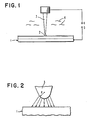
- FIG. 1 is a schematic illustration of the apparatus for producing fine lines of the invention.
- FIG. 2 is a schematic illustration of the current flow at the tip of the stylus in the apparatus of the invention.
- the invention is a simplified approach to fabrication of very narrow lines.
- the formation of fine, as small as 0,8 nanometers wide, lines on a substrate is provided by the invention by dissociating a gas using a relatively low-energy electron beam where the electron energy involved is just sufficient to dissociate the gas molecules.
- the electron energy involved is in the range of 1 electron volt to 100 electron volts and provides enough energy to accomplish the dissociation without the risk of electron scattering from the surface.
- the current passes through the gas between a point that concentrates the electrons, and the substrate.
- the gas is ambient in the vicinity and thus is in the space between the point and the substrate and adsorbed on the substrate.
- a gas molecule can be dissociated when it is struck by an electron of sufficient energy so as to leave a residue that on further processing can be converted into lines.
- a group of metal bearing gases can provide metal lines and organic molecular gases can provide carbon lines and common semiconductor dopant containing gases can provide semiconductor dopants.
- the current for minimal linewidth is tuned to the minimum electron energy required for the dissociation of the particular gas employed, including a slight addition for system losses.
- a current from a stylus having a point with a radius of the order of 5 nanometers can provide lines of the order of 8 to 10 nanometers.
- Tunneling current from a point to a surface has been employed in the art to provide very close topographical information about a surface.
- the apparatus employing this principle has come to be known in the art as the Scanning Tunneling Microscope and is described in Physical Review Letters, Vol. 49, No. 1, p. 57.
- Apparatus for practicing the invention will bear some resemblance to the Scanning Tunneling Microscope apparatus but will differ in that the current is sent through uniformly replenished gas where the electron energy is just above the energy required to dissociate the gas molecules.
- the apparatus namely and substrate, will have means of providing current between them.
- the tip of the stylus will be modified to produce the proper current concentration and means will be provided to maintain a gas, the molecules of which will dissociate in the current. Under proper conditions where a molecular monolayer is adsorbed (of the order of 1015 cm ⁇ 2),one dissociation molecular event for each 10 electrons may be expected.
- a substrate 1 on which a fine line 2 is to be formed is in position under a stylus 3.
- the separation between the stylus 3 and the substrate 1 depends on the stylus radius, the energy of the electrons, and the current.
- a source of voltage provided by power supply techniques standard in the art is introduced between two terminals 4 and 5 to sustain the current flow between the stylus 3 and the substrate 1.
- a dissociatable molecular gas 6 is maintained in the region between the stylus 3 and substrate 1. This is accomplished by merely providing an ambient of the gas 6 in the vicinity of the stylus 3.
- the gas pressure of gas 6 should be high enough to maintain at least a monolayer of molecules of gas 6 on the surface of substrate 1.
- FIG. 2 a schematic illustration is provided of the details of the current flow at the tip of the stylus 3.
- the details of the tip of the stylus 3 and the separation from the substrate 1 are of importance in the invention in that the energy involved in dissociating the gas in the quantum mechanical tunneling current is achieved through the radius of the tip and the separation for a given current value.
- the tip of the stylus 3 has a radius labelled R and the tip is separated at its closest point from the substrate 1 by a distance S.
- the radius R may, for most applications, be of the order of one nanometer. Tunneling current stylus tips of this size are common practice in the scanning tunneling electron microscope art.
- the radius R could be as small as one atomic diameter but at the present state of the art, however, a method of reliably forming a point that is one atomic diameter has not been achieved.
- Equation 1 W ⁇ S (R + S) ⁇
- the field at the tip of the stylus 3 should be no greater than in the vicinity of 107 - 108 volts per centimeter to prevent material decomposition of the tip.
- the lowest electron energy should be of the amount of energy necessary to dissociate a molecule of the gas 6 with allowance for some system losses.
- the highest tolerable electron energy would be governed by substrate backscattering. This higher value, however, if not limited by line definition, should not be so high that sputtering would occur, and hence it is necessary to stay below a field where the tip of the stylus 3 comes apart.
- the electron energy must be above the energy required to cause the molecules of the gas 6 to dissociate. Since there are different energies for different gases, the chemistry of the gas 6 provides some current flexibility.
- the gas 6 may dissociate and leave as the line 2 a residue, or it could create the line 2 as the product of further processing such as by locally changing a coating on the substrate 1 under the tip of the stylus 3.
- the gas 6 should preferably be a large molecular gas, such as trimethylaluminum A1 (CH3)3, tungsten hexafluoride WF6, boron trifluoride BF3, tungsten hexacarbonyl W (CO)6, disilane Si2H6, nickel hexacarbonyl Ni (CO)6 and Arsine AsH3.
- a large molecular gas such as trimethylaluminum A1 (CH3)3, tungsten hexafluoride WF6, boron trifluoride BF3, tungsten hexacarbonyl W (CO)6, disilane Si2H6, nickel hexacarbonyl Ni (CO)6 and Arsine AsH3.
- Each gas has a specific dissociation energy and the electrons of the field are arranged to closely match the necessary energy.
Landscapes
- Chemical & Material Sciences (AREA)
- Engineering & Computer Science (AREA)
- Physics & Mathematics (AREA)
- Nanotechnology (AREA)
- Analytical Chemistry (AREA)
- Mechanical Engineering (AREA)
- Crystallography & Structural Chemistry (AREA)
- General Chemical & Material Sciences (AREA)
- Metallurgy (AREA)
- Organic Chemistry (AREA)
- Health & Medical Sciences (AREA)
- Plasma & Fusion (AREA)
- Chemical Kinetics & Catalysis (AREA)
- Toxicology (AREA)
- Materials Engineering (AREA)
- Manufacturing & Machinery (AREA)
- Mathematical Physics (AREA)
- Theoretical Computer Science (AREA)
- General Physics & Mathematics (AREA)
- Condensed Matter Physics & Semiconductors (AREA)
- Chemical Vapour Deposition (AREA)
- Internal Circuitry In Semiconductor Integrated Circuit Devices (AREA)
Applications Claiming Priority (2)
| Application Number | Priority Date | Filing Date | Title |
|---|---|---|---|
| US06/626,178 US4550257A (en) | 1984-06-29 | 1984-06-29 | Narrow line width pattern fabrication |
| US626178 | 1984-06-29 |
Publications (3)
| Publication Number | Publication Date |
|---|---|
| EP0166308A2 EP0166308A2 (en) | 1986-01-02 |
| EP0166308A3 EP0166308A3 (en) | 1989-02-08 |
| EP0166308B1 true EP0166308B1 (en) | 1991-12-27 |
Family
ID=24509285
Family Applications (1)
| Application Number | Title | Priority Date | Filing Date |
|---|---|---|---|
| EP85107252A Expired - Lifetime EP0166308B1 (en) | 1984-06-29 | 1985-06-14 | Apparatus and method for narrow line width pattern fabrication |
Country Status (4)
| Country | Link |
|---|---|
| US (1) | US4550257A (enExample) |
| EP (1) | EP0166308B1 (enExample) |
| JP (1) | JPS6118156A (enExample) |
| DE (1) | DE3584994D1 (enExample) |
Families Citing this family (27)
| Publication number | Priority date | Publication date | Assignee | Title |
|---|---|---|---|---|
| US4566937A (en) * | 1984-10-10 | 1986-01-28 | The United States Of America As Represented By The United States Department Of Energy | Electron beam enhanced surface modification for making highly resolved structures |
| DE3570012D1 (en) * | 1985-01-29 | 1989-06-08 | Ibm | Field-emission scanning auger electron microscope |
| US4618767A (en) * | 1985-03-22 | 1986-10-21 | International Business Machines Corporation | Low-energy scanning transmission electron microscope |
| US4785189A (en) * | 1985-04-29 | 1988-11-15 | International Business Machines Corporation | Method and apparatus for low-energy scanning electron beam lithography |
| ATE66092T1 (de) * | 1986-12-07 | 1991-08-15 | Lasarray Holding Ag | Verfahren und vorrichtung zur erzeugung von materialstrukturen im bereich atomarer dimensionen. |
| EP0290647B1 (en) * | 1987-05-12 | 1991-07-24 | International Business Machines Corporation | Oscillating quartz atomic force microscope |
| US4844945A (en) * | 1988-05-18 | 1989-07-04 | Hewlett-Packard Company | Process for producing patterns in dielectric layers formed by plasma enhanced chemical vapor deposition (PECVD) |
| JPH02173278A (ja) * | 1988-12-26 | 1990-07-04 | Hitachi Ltd | 微細加工方法及びその装置 |
| SU1833046A1 (ru) * | 1989-05-12 | 1996-10-20 | Институт Радиотехники И Электроники Ан Ссср | Сканирующий туннельный микроскоп |
| US5015323A (en) * | 1989-10-10 | 1991-05-14 | The United States Of America As Represented By The Secretary Of Commerce | Multi-tipped field-emission tool for nanostructure fabrication |
| US5021672A (en) * | 1989-12-22 | 1991-06-04 | E. I. Du Pont De Nemours And Company | Etching of nanoscale structures |
| DE69131528T2 (de) * | 1990-05-30 | 2000-05-04 | Hitachi, Ltd. | Verfahren und Vorrichtung zur Behandlung eines sehr kleinen Bereichs einer Probe |
| US5369372A (en) * | 1990-12-13 | 1994-11-29 | Interuniversitair Micro Elektronica Centrum Vzw | Method for resistance measurements on a semiconductor element with controlled probe pressure |
| US5047649A (en) * | 1990-10-09 | 1991-09-10 | International Business Machines Corporation | Method and apparatus for writing or etching narrow linewidth patterns on insulating materials |
| US5304535A (en) * | 1990-10-29 | 1994-04-19 | E. I. Du Pont De Nemours And Company | Etching of nanoscale structures on high temperature superconductors |
| US5204588A (en) * | 1991-01-14 | 1993-04-20 | Sony Corporation | Quantum phase interference transistor |
| US5397420A (en) * | 1991-03-03 | 1995-03-14 | Nippondenso Co., Ltd. | Fine structure forming device |
| JP3270165B2 (ja) * | 1993-01-22 | 2002-04-02 | セイコーインスツルメンツ株式会社 | 表面分析及び加工装置 |
| JP3054900B2 (ja) * | 1993-03-10 | 2000-06-19 | セイコーインスツルメンツ株式会社 | 微細加工装置 |
| US5474640A (en) * | 1993-07-19 | 1995-12-12 | Applied Materials, Inc. | Apparatus for marking a substrate using ionized gas |
| US5674409A (en) * | 1995-03-16 | 1997-10-07 | International Business Machines Corporation | Nanolithographic method of forming fine lines |
| KR100331451B1 (ko) * | 2000-05-10 | 2002-04-09 | 윤종용 | 탄소 함유 물질을 이용한 재기록 가능한 데이타 스토리지및 그 기록/재생 방법 |
| DE10230675B4 (de) * | 2002-07-04 | 2007-01-25 | Infineon Technologies Ag | Verfahren zur Herstellung von Phasenschiebermasken |
| US20040060904A1 (en) * | 2002-09-30 | 2004-04-01 | International Business Machines Corporation | Tool having a plurality of electrodes and corresponding method of altering a very small surface |
| US20050016954A1 (en) * | 2003-07-25 | 2005-01-27 | International Business Machines Corporation | System and methods of altering a very small surface area |
| US8053037B2 (en) * | 2003-11-12 | 2011-11-08 | International Business Machines Corporation | Device and method for patterning structures on a substrate |
| US9298285B2 (en) * | 2013-12-05 | 2016-03-29 | Wacom Co., Ltd. | Stylus tip shape |
Family Cites Families (7)
| Publication number | Priority date | Publication date | Assignee | Title |
|---|---|---|---|---|
| US3658572A (en) * | 1968-11-05 | 1972-04-25 | Westinghouse Electric Corp | Pyrolytic coatings of molybdenum sulfide by plasma jet technique |
| US4197332A (en) * | 1977-10-26 | 1980-04-08 | International Business Machines Corporation | Sub 100A range line width pattern fabrication |
| US4316093A (en) * | 1979-02-12 | 1982-02-16 | International Business Machines Corporation | Sub-100A range line width pattern fabrication |
| CH643397A5 (de) * | 1979-09-20 | 1984-05-30 | Ibm | Raster-tunnelmikroskop. |
| US4382186A (en) * | 1981-01-12 | 1983-05-03 | Energy Sciences Inc. | Process and apparatus for converged fine line electron beam treatment of objects |
| DE3235064A1 (de) * | 1982-09-22 | 1984-03-22 | Siemens AG, 1000 Berlin und 8000 München | Tunnelkathodenmaske fuer die elektronenlithografie, verfahren zu ihrer herstellung und verfahren zu ihrem betrieb |
| DE3483982D1 (de) * | 1983-06-29 | 1991-02-28 | Siemens Ag | Verfahren zur herstellung einer elektrisch leitfaehigen verbindung und vorrichtung zur durchfuehrung eines solchen verfahrens. |
-
1984
- 1984-06-29 US US06/626,178 patent/US4550257A/en not_active Expired - Lifetime
-
1985
- 1985-04-18 JP JP60081517A patent/JPS6118156A/ja active Granted
- 1985-06-14 DE DE8585107252T patent/DE3584994D1/de not_active Expired - Lifetime
- 1985-06-14 EP EP85107252A patent/EP0166308B1/en not_active Expired - Lifetime
Non-Patent Citations (4)
| Title |
|---|
| APPLIED PHYSICS LETTERS vol. 46, no. 9, 1st May 1985, pages 832-834, Woodbury, New York, US; M. RINGER et al.: " Nanometer lithography with the scanning tunneling microscope " * |
| FERNSEH & KINO TECHNIK vol. 37, no. 3, March 1983, page 102, " Lithographie mit schnellen Elektronen " * |
| H-W FINK, IBM J. Res. Develop. Vol. 30 No. 5, p. 460-465, 1986, September * |
| OPTICS AND LASER TECHNOLOGY vol. 16, no. 6, Feb. 1984, pages 37-39, Exeter, GB; K.G. IBBS et al.: " Laser doping : bipolar structures in silicon " * |
Also Published As
| Publication number | Publication date |
|---|---|
| US4550257A (en) | 1985-10-29 |
| EP0166308A2 (en) | 1986-01-02 |
| DE3584994D1 (de) | 1992-02-06 |
| JPH039615B2 (enExample) | 1991-02-08 |
| EP0166308A3 (en) | 1989-02-08 |
| JPS6118156A (ja) | 1986-01-27 |
Similar Documents
| Publication | Publication Date | Title |
|---|---|---|
| EP0166308B1 (en) | Apparatus and method for narrow line width pattern fabrication | |
| US8937001B2 (en) | Patterning of nanostructures | |
| US5015323A (en) | Multi-tipped field-emission tool for nanostructure fabrication | |
| Utke et al. | Gas-assisted focused electron beam and ion beam processing and fabrication | |
| US6924493B1 (en) | Ion beam lithography system | |
| McCord et al. | Direct deposition of 10‐nm metallic features with the scanning tunneling microscope | |
| US6632483B1 (en) | Ion gun deposition and alignment for liquid-crystal applications | |
| US20100323113A1 (en) | Method to Synthesize Graphene | |
| EP0795622A1 (en) | Amorphous multi-layered structure and method of making the same | |
| JPH04288815A (ja) | パターン形成方法及び装置 | |
| US5935639A (en) | Method of depositing multi-layer carbon-based coatings for field emission | |
| Chang et al. | Nanostructure technology | |
| JP4636476B2 (ja) | 電子サイクロトロン共鳴プラズマによる電子放出カーボンフィルムの蒸着方法 | |
| KR100445105B1 (ko) | 가스 클러스터 이온빔을 이용한 아이.티.오 박막 표면처리시스템 및 그 방법 | |
| Melngailis | Ion sources for nanofabrication and high resolution lithography | |
| US20040084152A1 (en) | Apparatus for large-scale diamond polishing | |
| US20180245213A1 (en) | Methods of forming films | |
| US4538067A (en) | Single grid focussed ion beam source | |
| KR100462055B1 (ko) | 물질의 결정구조를 이용한 패턴 형성 방법 및 장치 | |
| KR970701274A (ko) | 기질(substrate)을 코팅하는 방법 및 장치 | |
| Melngailis et al. | Focused ion beam induced deposition | |
| Floreani et al. | Operation of high power field emitters fabricated with electron beam deposition and concept of a miniaturised free electron laser | |
| US20060118735A1 (en) | Lithography systems and methods for operating the same | |
| Melngailis | Focused ion beam fabrication of microelectronic structures | |
| Tian | Sub 10-nm Nanopantography and Nanopattern Transfer Using Highly Selective Plasma Etching |
Legal Events
| Date | Code | Title | Description |
|---|---|---|---|
| PUAI | Public reference made under article 153(3) epc to a published international application that has entered the european phase |
Free format text: ORIGINAL CODE: 0009012 |
|
| AK | Designated contracting states |
Designated state(s): DE FR GB |
|
| 17P | Request for examination filed |
Effective date: 19860424 |
|
| PUAL | Search report despatched |
Free format text: ORIGINAL CODE: 0009013 |
|
| AK | Designated contracting states |
Kind code of ref document: A3 Designated state(s): DE FR GB |
|
| 17Q | First examination report despatched |
Effective date: 19900117 |
|
| GRAA | (expected) grant |
Free format text: ORIGINAL CODE: 0009210 |
|
| AK | Designated contracting states |
Kind code of ref document: B1 Designated state(s): DE FR GB |
|
| REF | Corresponds to: |
Ref document number: 3584994 Country of ref document: DE Date of ref document: 19920206 |
|
| ET | Fr: translation filed | ||
| PLBE | No opposition filed within time limit |
Free format text: ORIGINAL CODE: 0009261 |
|
| STAA | Information on the status of an ep patent application or granted ep patent |
Free format text: STATUS: NO OPPOSITION FILED WITHIN TIME LIMIT |
|
| 26N | No opposition filed | ||
| REG | Reference to a national code |
Ref country code: GB Ref legal event code: IF02 |
|
| PGFP | Annual fee paid to national office [announced via postgrant information from national office to epo] |
Ref country code: GB Payment date: 20040601 Year of fee payment: 20 |
|
| PGFP | Annual fee paid to national office [announced via postgrant information from national office to epo] |
Ref country code: DE Payment date: 20040615 Year of fee payment: 20 |
|
| PGFP | Annual fee paid to national office [announced via postgrant information from national office to epo] |
Ref country code: FR Payment date: 20040621 Year of fee payment: 20 |
|
| PG25 | Lapsed in a contracting state [announced via postgrant information from national office to epo] |
Ref country code: GB Free format text: LAPSE BECAUSE OF EXPIRATION OF PROTECTION Effective date: 20050613 |
|
| REG | Reference to a national code |
Ref country code: GB Ref legal event code: PE20 |