EP0165600B1 - Input/output bus for computer - Google Patents
Input/output bus for computer Download PDFInfo
- Publication number
- EP0165600B1 EP0165600B1 EP19850107568 EP85107568A EP0165600B1 EP 0165600 B1 EP0165600 B1 EP 0165600B1 EP 19850107568 EP19850107568 EP 19850107568 EP 85107568 A EP85107568 A EP 85107568A EP 0165600 B1 EP0165600 B1 EP 0165600B1
- Authority
- EP
- European Patent Office
- Prior art keywords
- bus
- data
- computer
- units
- parcel
- Prior art date
- Legal status (The legal status is an assumption and is not a legal conclusion. Google has not performed a legal analysis and makes no representation as to the accuracy of the status listed.)
- Expired - Lifetime
Links
Images


Classifications
-
- G—PHYSICS
- G06—COMPUTING; CALCULATING OR COUNTING
- G06F—ELECTRIC DIGITAL DATA PROCESSING
- G06F13/00—Interconnection of, or transfer of information or other signals between, memories, input/output devices or central processing units
- G06F13/14—Handling requests for interconnection or transfer
- G06F13/20—Handling requests for interconnection or transfer for access to input/output bus
- G06F13/24—Handling requests for interconnection or transfer for access to input/output bus using interrupt
- G06F13/26—Handling requests for interconnection or transfer for access to input/output bus using interrupt with priority control
-
- G—PHYSICS
- G06—COMPUTING; CALCULATING OR COUNTING
- G06F—ELECTRIC DIGITAL DATA PROCESSING
- G06F13/00—Interconnection of, or transfer of information or other signals between, memories, input/output devices or central processing units
- G06F13/14—Handling requests for interconnection or transfer
- G06F13/20—Handling requests for interconnection or transfer for access to input/output bus
- G06F13/28—Handling requests for interconnection or transfer for access to input/output bus using burst mode transfer, e.g. direct memory access DMA, cycle steal
-
- G—PHYSICS
- G06—COMPUTING; CALCULATING OR COUNTING
- G06F—ELECTRIC DIGITAL DATA PROCESSING
- G06F13/00—Interconnection of, or transfer of information or other signals between, memories, input/output devices or central processing units
- G06F13/14—Handling requests for interconnection or transfer
- G06F13/36—Handling requests for interconnection or transfer for access to common bus or bus system
- G06F13/362—Handling requests for interconnection or transfer for access to common bus or bus system with centralised access control
- G06F13/364—Handling requests for interconnection or transfer for access to common bus or bus system with centralised access control using independent requests or grants, e.g. using separated request and grant lines
-
- G—PHYSICS
- G06—COMPUTING; CALCULATING OR COUNTING
- G06F—ELECTRIC DIGITAL DATA PROCESSING
- G06F13/00—Interconnection of, or transfer of information or other signals between, memories, input/output devices or central processing units
- G06F13/38—Information transfer, e.g. on bus
- G06F13/42—Bus transfer protocol, e.g. handshake; Synchronisation
- G06F13/4204—Bus transfer protocol, e.g. handshake; Synchronisation on a parallel bus
- G06F13/4208—Bus transfer protocol, e.g. handshake; Synchronisation on a parallel bus being a system bus, e.g. VME bus, Futurebus, Multibus
- G06F13/4217—Bus transfer protocol, e.g. handshake; Synchronisation on a parallel bus being a system bus, e.g. VME bus, Futurebus, Multibus with synchronous protocol
-
- G—PHYSICS
- G06—COMPUTING; CALCULATING OR COUNTING
- G06F—ELECTRIC DIGITAL DATA PROCESSING
- G06F15/00—Digital computers in general; Data processing equipment in general
- G06F15/16—Combinations of two or more digital computers each having at least an arithmetic unit, a program unit and a register, e.g. for a simultaneous processing of several programs
- G06F15/163—Interprocessor communication
- G06F15/17—Interprocessor communication using an input/output type connection, e.g. channel, I/O port
Landscapes
- Engineering & Computer Science (AREA)
- Theoretical Computer Science (AREA)
- Physics & Mathematics (AREA)
- General Engineering & Computer Science (AREA)
- General Physics & Mathematics (AREA)
- Computer Hardware Design (AREA)
- Software Systems (AREA)
- Bus Control (AREA)
Description
- The present invention pertains in general to computer technology and in particular to a communication bus for providing data transfer between a computer and one or more peripheral units.
- The central processor of a computer carries out the functions of data processing and operand manipulation. These functions can be designed to be carried out at an extremely fist rate. But to take advantage of the maximum execution rate of the processor, data must be delivered to the processor and returned from it at the rate required by the processor. Data can be received from numerous sources such as tape drives, disk drives and real time data. An input/output bus must be used to transmit the data to and from the central processor. Typically there are numerous types of devices that must be connected to an input/output bus. These numerous devices as well as the processor itself compete for the use of the bus.
- Conventional input/output buses transfer an address together with each unit of data that is transmitted through the bus. Such a technique simplifies the interfacing to the bus and makes it easy to handle interruptions to the data transfer. However, this method of data transfer has a substantial overhead which seriously reduces the effective bandwidth of the data transfer through the bus. The limited bandwidth of a conventional bus can prevent the central processor from being used to its fullest capability.
- In COMPUTER DESIGN, vol. 23, no. 7, June 1984, pages 129-135, Littleton, Massachusetts, US; G.P. WHITE: "Bus structure eases multiprocessor integration" a bus system is described where the bus master in the first phase of a transaction transfers the destination address and the length of a block and in subsequent phases of the transaction transfers sucsessive words.
- The present invention concerns a method and a system as claimed respectively in claim 1 and claim 2.
- For a more complete understanding of the present invention and the advantages thereof reference is now made to the following description taken in conjunction with the following drawings in which:
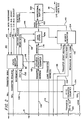
- FIGURE 1 is a functional block diagram of a computer system which includes a computer having a memory control unit, a memory array and a central processing unit, the computer communicating through an input/output bus to a plurality of peripheral units which include input/output processors and a service processor, the system further including an interrupt bus for interconnecting various elements of the system,
- FIGURE 2 is a functional block diagram of an input/output bus interface for a peripheral unit such as an input/output processor as shown in FIGURE 1,
- FIGURE 3 is an illustration of a header parcel which is generated by one of the peripheral units and transmitted through the input/output processor shown in FIGURE 1,
- FIGURE 4 is a timing illustration showing the sequence of requesting the input/output bus, granting use of the bus, transmitting the header parcel followed by transmission of the sections of data which are termed data parcels,
- FIGURE 5 is a functional block diagram illustrating a circuit for providing transfer of data between the input/output bus and the memory control unit illusrated in FIGURE 1,
- FIGURE 6 is an illustration of a sender unit for interfacing with the interrupt bus shown in FIGURE 1, and
- FIGURE 7 is a functional block diagram showing a receiver unit for interfacing with the interrupt bus shown in FIGURE 1.
- The present invention is a method and circuit for providing data communication between the various elements of a computer system.
- Referring now to FIGURE 1 there is illustrated a
computer system 10 which includes acomputer 12, acommunication bus 14, aninterrupt bus 16 and a plurality of peripheral units including input/output processors 18 and 20 and aservice processor 22. The combination ofcommunication bus 14 and theinterrupt bus 16 comprises an input/output bus for thecomputer system 10. - The
computer 12 includes amemory control unit 24 which is connected to both of thebuses memory array unit 26 is connected to transfer data through amemory bus 28 to and from thememory control unit 24. Acentral processor unit 30 is connected through acommunication bus 32 to thememory control unit 24. - Within the
memory control unit 24 there is included acommunication bus arbiter 38 and aninterrupt bus arbiter 40. Each of the peripheral units, such asprocessors arbiter 38 by both a request and a grant line.Processor 18 is connected toarbiter 38 through arequest line 42 and agrant line 44. The processor 20 is connected to thearbiter 38 through arequest line 46 and agrant line 48. Theprocessor 22 is connected to thearbiter 38 through arequest line 50 and agrant line 52. The request lines transfer signals from the peripheral unit processor to thearbiter 38 while the grant lines transfer a grant signal from thearbiter 38 to each of the individual processors. - Additional request and
grant lines memory control unit 24. - An address/
data bus 58 provides a plurality of paths for data transfer. Thebus 58 is connected in parallel to thememory control unit 24 and theprocessors Bus 58 is preferably a 64 bit wide data path which provides bidirectional transfer of data. Additional processors can be connected to thebus 58 with each additional processor also having a corresponding request and grant line connected to thebus arbiter 38. Adata handshake line 60 provides a plurality of contral lines connecting thememory control unit 24 and the various processors. The data handshake lines provide conventional signals to permit the transfer of data between the processors and the memory control unit. - The
communication bus 14 comprises the collection of lines and buses 42-60. - The
interrupt bus 16 comprises a plurality of lines.Interrupt vector lines 66 are a group of 8 parallel lines which provide a bidirectional parallel transfer of an 8 bit vector signal which corresponds to one of the units connected to thelines 66. Thelines 66 are connected to thecentral processing unit 30, theinterrupt bus arbiter 40 and to theprocessors bus 14. Each of the units on theinterrupt bus 16 has a corresponding pair of request and grant lines which are connected to thearbiter 40.Processor 18 is connected to thearbiter 40 through arequest line 68 and a grant line 70. The processor 20 is connected to thearbiter 40 through arequest line 72 and agrant line 74. Theservice processor 22 is connected to theinterrupt bus arbiter 40 through arequest line 76 and agrant line 78. Thecentral processing unit 30 is also connected to thearbiter 40 through arequest line 80 and agrant line 82. Each of the units on theinterrupt bus 16 is further connected through a common group ofinterrupt handshake lines 84 for providing control of the transmission of interrupt vector signals through theinterrupt bus 16. - Further referring to FIGURE 1, the combination of the
communication bus 14 and theinterrupt bus 16 comprises the overall input/output bus for thecomputer system 10. Various processors are added to the input/output bus as required for a particular implementation. The input/output bus serves as the only path for input/output traffic for thesystem 10. Thebuses computer system 10. Thevarious processors communication bus 14, function as masters of the bus while thememory control unit 24 is the slave. A transfer request is initiated by a processor, such as for example,processor 18, by generating a request signal that is transmitted throughline 42 to thearbiter 38. When thebus 14 becomes available, thearbiter 38 provides a grant signal throughline 44 back to theprocessor 18. Theprocessor 18 then sends a header parcel, further described below, through thebus 58 to thememory control unit 24. Following transmittal of this header parcel, data is transmitted as data parcels through thebus 58. The data transfer can be either from theprocessor 18 to thememory control unit 24 or from thememory control unit 24 to the input/output processor 18. In any case the data being transferred ultimately starts or ends at thememory array 26. Data communication operation for thecomputer system 10 is described in further detail below. - Further referring to FIGURE 1, the interrupt
bus 16 provides a means of communication between thevarious processors central processing unit 30. Interrupt requests can be transmitted from any one of these units to any other one of the units. The primary function of the interrupt requests are to signal completion of a task, request action or to indicate an error condition. Briefly, the interruptbus 16 functions much like thecommunication bus 14 described above. A peripheral unit, such asprocessor 18, initiates the interrupt procedure by transmitting a request signal through itsrequest line 68 to the interruptbus arbiter 40. When thearbiter 40 determines that the interruptbus 16 is available, it provides a grant signal through the line 70 to theprocessor 18. Upon receipt of the grant, theprocessor 18 places an interrupt vector, an eight bit code, on the interruptvector lines 66. This interrupt vector signal is transmitted to all of the other units on the interruptbus 16. However, only one of the units will recognize the vector as being directed to that particular unit. The receiving unit will acknowledge receipt of the vector and then complete the required interrupt operation. The required interfacing operations between the transmitting and receiving units is controlled by signals transmitted through the handshake lines 84. The interrupt operation forcomputer system 10 is described below in further detail. - Referring now to FIGURE 2 there is illustrated a
typical interface circuit 90 for interfacing a peripheral unit, such as one of theprocessors communication bus 14. Theinterface circuit 90 includes astate machine controller 92 which generates control signals in response to various inputs. Thecontroller 92 is connected to thedata handshake line 60, the I/Obus grant line 44 and therequest line 42. For the present example theinterface circuit 90 is used within the input/output processor 18, however, a similar interface circuit is used with each of the other processors shown in FIGURE 1. Agroup 91 of interface lines connects theinterface circuit 90 to other sections of theprocessor 18. In operation, thestate machine controller 92 receives a data transfer request via a line 94 from theprocessor 18. When a data transfer is completed, a transfer done command is transmitted to theprocessor 18 via a line 96. - The
controller 92 is further connected through aline 98 to control the operation of abuffer 100. Thebuffer 100 provides bidirectional data transfer between the address/data bus 58 and aninternal data bus 102. Thebuffer 100, for the described embodiment, stores a longword of data which is 64 bits. - The
interface circuit 90 further includes a data store 104 which is connected to transmit to or receive data from thebus 102. A read or write command is transmitted from thecontroller 92 through aline 106 connected to the data store 104. - The
processor 18 provides a data transfer address through aline 108 to an address register/counter 110. A load transfer address command is generated by theprocessor 18 and transmitted through a line 112 to theaddress register counter 110. Thecounter 110 receives an initial address and adds a constant number to this address to produce a sequence of addresses which are transmitted through aline 114 to the data store 104. The first address and any subsequent address can be selected by thecontroller 92 through aline 116. Data is transferred between theprocessor 18 and the data store 104 through abus 118. - The
processor 18, in preparing a transfer request, produces a count of the number of bytes in the data block for the transfer request. This count of the size of the block to be transferred is provided as a transfer byte out count through aline 122 to abyte transfer counter 124. The count is entered into thecounter 124 through a load command transmitted through a line 126. Thecontroller 92 monitors each transfer of data through thebus 58. As each group of bytes comprising a data parcel is transferred, thecounter 24 is decremented by that number of bytes by operation of a command transmitted through adecrement line 128 from thecontroller 92 to thecounter 124. The transfer of data is completed when the count withincounter 124 equals 0. A count = 0 signal is then transmitted fromcounter 124 through aline 130 to thecontroller 92 to signal the completion of the data transaction. - A remaining byte count, the count within the
counter 124, can be transmitted through aline 132 to aheader generator 134 when a full transaction is not completed. Theprocessor 18 further provides a data transfer start address through aline 136 to theheader generator 134. In addition theprocessor 18 provides a command code through aline 138 specifying a read, write or other possible transaction to theheader generator 134. After a header parcel, described further below, has been prepared by theheader generator 134 and thestate machine controller 92 has obtained use of thecommunication bus 14, the header parcel is transmitted from theheader generator 134 through aline 140 onto theinternal data bus 102 for transfer through thebuffer 100 to the I/O bus 58. Thecontroller 92 provides a command to output the header parcel and this command is transmitted through aline 144 to theheader generator 134. The detailed operation ofinterface circuit 90 is further described below. - The header parcel noted above is shown in further detail in FIGURE 3. The header parcel is indicated generally by the
reference numeral 146. Theparcel 146 includes a physical address field 148 which comprises bits 0-30. The physical address is the starting address for the transaction. Acommand field 150 comprises bits 40-42 and specifies the type of transaction, such as read or write. There is further included abyte count field 152 which extends to cover bits 48-63. The lower three bits of thebyte count field 152 determine the location of the first byte within the first data parcel transmitted in a data transfer. The remaining bit locations withinheader parcel 146 are reserved. - A timing sequence for obtaining use of the
communication bus 14 and transferring data is illustrated in FIGURE 4. Each of the time segments comprises a clock tick in which one event is carried out. The first step in a data transfer comprises transmitting a request to thearbiter 38. Arequest 158 is sent during a clock tick. Thearbiter 38 evaluates various factors including the present use of thebus 14 and the other units requesting to use thebus 14. When appropriate, thearbiter 38 provides agrant 160 to the requesting processor. The requesting processor then transmits a preformed header parcel 162 in the clock tick following the grant. Immediately following the header parcel 162 there is a series of data transfers ofdata parcels 164, 166. . . until the data block is completely transferred or there is an interrupt of the transfer process. In a preferred embodiment of the invention each of the clock ticks has a period of 100 nanoseconds. - Referring to FIGURE 5 there is shown a memory control
unit interface circuit 172 which connects to thecommunication bus 14 for operating in conjunction with theinterface circuit 90 for each of the peripheral units. Thecircuit 172 includes an address register counter 174 which is connected to receive addresses from thebus 58. The counter 174 further receives an increment command through aline 176 which causes the counter 174 to produce a sequence of physical longword addresses which are transmitted through aline 178 for delivery to thememory array 26. Aword counter 180 is connected to thebus 58 for receiving the count which is transmitted as a part of theheader parcel 146. Thecounter 180 transmits a longword count through aline 182 for use by thememory control unit 24. Thecircuit 172 further includes acontrol latch 184 which receives the command code that is transmitted as a part of theheader parcel 146 through thebus 58. This command is transmitted through aline 186 to thememory control unit 24. - Data received from the
bus 58 is input to adata input latch 188 which is connected to transfer the data to a bidirectionalinternal bus 190. Adata output latch 192 is connected to transfer data from theinternal data bus 190 to the address/data bus 58. - The operation of the
communication bus 14 for providing data transfer between thememory control unit 24 and any one of the peripheral units connected to thebus 14 is now described in reference to FIGURES 1-5. A data transfer request is initiated by a peripheral unit, such as one of theprocessors Processor 18 is used for the present example. A data transfer can be either from theprocessor 18 into thememory control unit 24 or from thememory control unit 24 to the input/output processor 18. The first step in a data transfer is to generate a header parcel as shown in FIGURE 3. Theprocessor 18 has a physical address for a data block transfer. This physical address is transmitted throughline 108 to theaddress register counter 110. This address is then transferred through line 142 into theheader generator 134 to form field 148 of theheader parcel 146. The size, byte count, of the data transfer is transmitted throughline 122 to thecounter 124. This byte count is transmitted throughline 132 into theheader generator 134 to comprise thefield 152 within theheader parcel 146. The command code to determine whether this transfer is a read, write or other operation is transmitted fromprocessor 18 throughline 138 into theheader generator 134. This command code becomesfield 150 within theheader parcel 146. - After the header parcel is prepared, the
controller 92 initiates a request command through therequest line 42 to thearbiter 38. This corresponds to therequest 158 shown in FIGURE 4. If thebus 14 is not in use then thearbiter 38 immediately provides a grant, such as 160, which is transmitted throughline 44 to thecontroller 92. But if other peripheral units are competing withprocessor 18 for use of thebus 14, thearbiter 38 must determine which request is the first to receive use of thebus 14. This is primarily done on a round-robin or rotary basis among the similar processors on thebus 14. Basically when there is contention, no processor will receive the bus twice before another processor has received it once. There may further be an allocation of priorities among various units for access to thebus 14. For example, theservice processor 22 typically transfers much smaller units of data than theprocessor 18. Therefore, theprocessor 22 may be assigned a higher priority for accessing thebus 14. - After the
arbiter 38 sends the grant signal to thecontroller 92, an output header signal is transmitted throughline 144 to theheader generator 134. This causes the header parcel to be transferred from thegenerator 134 onto theinternal bus 102 to thebuffer 100. Thecontroller 92 then activates thebuffer 100 to transfer the header parcel onto the address/data bus 58 for transfer to thememory control unit 24. Upon receipt at theinterface circuit 172, the various fields in the header parcel are stored in appropriate locations. The physical address is stored in the address register counter 174. The count is stored in theword counter 180. The control code is stored in thecontrol latch 184. The control code that determines whether this a read, write or other operation is transmitted throughline 186 to another portion of thememory control unit 24 to activate an appropriate operation, such as read or write with respect to thememory array 26. - First, assume this to be a write operation. The I/
O processor 18 has provided data to the data store 104 throughline 118. The data store 104 functions as a buffer. A parcel of data, typically a longword, 64 bits, is transferred from the data store 104 to thebuffer 100 where it is passed to thebus 58 and then stored in theinput latch 188. The data parcel is then passed to theinternal data bus 190 where it is stored in thememory array 26 at the address provided by counter 174. Data parcels are sent in a similar fashion during each sequential clock tick, as shown in FIGURE 4. During each clock tick the counter 174 is sequenced to form a new address for storing the corresponding data parcel received during the clock tick. This process continues until the decreasing longword count in theword counter 180 reaches 0. This indicates completion of the data transfer. - If the data transfer operation, on the other hand, is a read, the address in the counter 174 is provided to read a block of data from the
memory array 26. The data block is returned to thedata output latch 192 as a data parcel which is transmitted through thebus 58, to thebuffer 100 for storage in the data store 104. When an appropriate size block of data is collected in the data store 104 it is then transmitted through theline 118 to the I/O processor 18. It is then typically stored on a disk or tape. The address in the counter 174 is sequenced to the next memory block to produce the next data parcel for transmission through thedata bus 58. This process is repeated until the count within theword counter 180 roaches 0. At this point the read operation is complete. - A typical data transaction between the
processor 18 and thememory control unit 24 comprises moving a 4K byte page of data. It is possible that this transaction may be terminated before completion by thearbiter 38 removing the grant signal online 44. This can occur if a higher priority peripheral unit or thecentral processor 30 requests use of thebus 14. This does not cause the loss of any data. Upon termination of the transfer, the address for the next data parcel is held in thecounter 110 which has been uniformly changed for each transfer of the data parcel. The number of bytes remaining to be transferred is maintained in thecounter 124. After the data transfer is broken, thestate machine controller 92 starts the process over again to complete the data transfer. A new header parcel is generated in theheader generator 134. The address in thecounter 110 is transferred vialine 114 to theheader generator 134 to produce the address portion of the header parcel. The count incounter 124 is transferred to thegenerator 134 for the data count field of the new header parcel. The command code remains the same. When thecontroller 92 receives a grant from thearbiter 38 the data transfer process is started again by the transmission of the header parcel throughbus 58 to theinterface 172. The transfer continues in the same manner as the method described above. This second transmission of the data block can either be carried through to completion or again can be interrupted. Any number of interruptions may occur but the data transfer process can be reinitiated each time to finally provide transfer for the complete data block. - The method of transferring data as described for the present invention provides a significantly greater bandwidth in comparison to previous techniques. This is due to the very small amount of overhead required for a large block transfer, which is the typical case. The only overhead required is for the header parcel. The required addresses at the
memory control unit 24 are generated within the unit itself. Breaks in the data transmission are readily handled by maintaining a running address and byte count for the data transfer at the originating unit, such asprocessor 18. Thus, an interruption in the data transfer process does not result in any loss of data and can be immediately reinitiated in the same fashion as an original transfer. This provides substantial flexibility in input/output communication by permitting the allocation of priorities of operation for various units. - The interrupt bus system is now described in reference to FIGURES 6 and 7. FIGURE 6 illustrates a
sender interface circuit 200 for operation with the interruptbus 16.Circuit 200 is described in reference to I/O processor 18 as an example. However, a similar sender interface circuit is required for each unit that interfaces to the interruptbus 16. A state interruptcontroller 202 generates a request signal at therequest line 68 and receives an interrupt grant signal through the line 70. As a part of the interrupthandshake lines 84 there is included an interrupt acknowledgeline 204 which is connected in common to each of the units on the interruptbus 16. The use of this line is further described in reference to FIGURE 7. - Vector data, comprising an 8 bit code, is generated by the
processor 18 and transmitted through a line 206 to avector register 208. The vector data signal transmitted to register 208 identifies a selected element of the computer system that is to receive an interrupt request. The vector data signal is loaded intoregister 208 in response to a load vector command transmitted through line 210. The vector data signal is transmitted fromvector register 208 to the interruptvector lines 66 in response to an enable signal generated by thecontroller 202 and transmitted through aline 212 to theregister 208. - Referring now to FIGURE 7 there is illustrated a receive
circuit 220 which forms a part of the interface to the interruptbus 16 for each of the units connected to the interrupt bus. Thecircuit 220 includes a state interruptcontroller 222 which generates the interrupt acknowledge signal atline 204. Thecontroller 222 further generates an interrupt received signal at aline 224 to activate the interrupt procedure within theprocessor 18. - The interrupt
vector lines 66 are connected to acomparator 226. A local vector signal is input at aline 228 by theprocessor 18 to identity the vector that is recognized by that particular unit on the interruptbus 16. Thecomparator 226 makes a comparison of the interrupt vector signal received atlines 66 with the local vector signal input atline 228 and upon detection of a comparison produces a vector compare signal which is transmitted through aline 230 to the interruptcontroller 222. An interruptline 232 provides an interrupt initiation signal indicating that an interrupt request had been transmitted through the interruptvector lines 66. This interrupt initiation signal atline 232 is transmitted to the state interruptcontroller 222. It serves essentially as an enable to receive the vector compare signal transmitted throughline 230. A clear interrupt signal is generated locally by theprocessor 18 and transmitted through aline 234 to thecontroller 222. The clear interrupt signal indicates that the function carried out in response to the interrupt request has been completed. - Operation of the interrupt bus is now described in reference to FIGURES 1, 6 and 7. For this description an example will be presented utilizing the I/
O processor 18 which includes theinterface circuits bus 16 begins with the generation of a vector data signal which is transmitted through line 206 to thevector register 208.State controller 202 applies a request signal to theline 68 for requesting use of the interruptbus 16. The request signal is received by the interruptbus arbiter 40 within thememory control unit 24. Thisarbiter 40 also functions essentially in a round-robin or rotary fashion when there is a conflict in requesting use of thebus 16. As with thearbiter 38, when there is a conflict the basic arbitration rule is that no requestor will have use of the bus twice before one requestor has it once. However, priority may be assigned to certain units to override this rotation scheme. - The
arbiter 40 awards the interruptbus 16 to the requestor by applying a grant signal to the interrupt grant line 70. In response to receipt of the grant thecontroller 202 applies an enable signal to theregister 208 for applying the interrupt vector signal to thelines 66. This vector is then transmitted to each of the other units connected to the interruptbus 16. However, each vector is recognized by only one unit. But a number of vectors may be transmitted to any one unit to produce different results. The vector signal is input to thecomparator 226 for comparison with the local vector signal to determine if the two vectors compare. At the time of making the grant, thearbiter 40 applies a signal to the interruptline 232 indicating that a valid interrupt vector request has been applied to the vector lines 66. If the interrupt signal atline 232 and the vector comparesignal line 230 are received concurrently at thecontroller 222 there is generated an interrupt acknowledge signal which is transmitted throughline 204 to each of the units on the interruptbus 16. The originating unit,processor 18 in this example, receives the interrupt acknowledge thereby verifying that the interrupt vector has been successfully transmitted and received. Thecontroller 222 further produces an interrupt received signal atline 224 for initiating theprocessor 18 to carry out the function specified by the interrupt request. During the time that an interrupt function is in process theprocessor 18 provides an interrupt signal throughline 232 indicating that the most recently received interrupt request is in process. This prevents a second interrupt from being received before the first is completed. Upon completion of the received interrupt, the interrupt signal atline 232 is returned to the noninterrupt state to permit receipt of another interrupt. - A particularly significant feature of the present invention is that any unit on the interrupt
bus 16 can transmit an interrupt request to any other unit on the interruptbus 16. There is no requirement to transmit the interrupts to any central location. This adds to the flexibility and speed of operation of thesystem 10.
Claims (2)
- A method for data communication via a bus (14) connecting a computer (12) to one or more peripheral units (18) which are selectively granted use of the bus (14) by a bus arbiter (38) for transferring data blocks (164) between the computer (12) and one of the peripheral units (18), wherein communication of data blocks (164) is initiated when a request is made to the bus arbiter (38) for use of the bus (14) by one of the peripheral units (18) and the bus arbiter (38) grants use of the bus (14) to the requesting peripheral unit (18), the method characterized in the steps of:
generating a header parcel (146) by an interface circuit (90) for said one peripheral unit (18), said header parcel (146) comprising an address (148) for a block (164) to be transferred between said computer (12) and said one peripheral unit (18), a count (152) indicating the size in units of said data block (164) and a command code (150) indicating whether the data block (164) transfer is a read from or write to said computer (12), for said data block (164),
transmitting said header parcel (146) from said interface circuit (90) for said one peripheral unit (18) via said bus (14) to said computer (12) after said step of granting,
sequentially transmitting units of said data block (164) via said bus (14) between said computer (12) and said peripheral unit (18),
maintaining by said interface circuit (90) for said one peripheral unit (18) a count of the number of said units of said data block (164) remaining to be transmitted between said computer (12) and said one peripheral unit (18),
terminating transfer of said data block (164) between said computer (12) and said one peripheral unit (18) prior to the transfer of the entirety of said data block (164) as a result of, for example, preemption of said bus (14) by other of said peripheral units (18, 20),
generating a new header parcel (146) by said interface circuit (90) for said one peripheral unit (18) to complete the transfer of said data block (164), said new header parcel (146) comprising a new address determined from said address for said data block (164) and said remaining count of the number of units of said data block (164) at the time of the terminating of said transfer of said data block (164), said remaining count and said command code, and
repeating said previous steps of requesting and granting, transmitting said new header parcel (146) from said interface circuit (90) for said one peripheral unit (18) to said computer (12), and
sequentially transmitting the remaining units of said data block (164) via said bus (14) between said computer (12) and said one peripheral unit (18). - An input/output bus system for providing communication of data blocks (164) between a computer (12) and one or more peripheral units (18) via a bus (14) wherein a bus arbiter (38) selectively grants use of the bus (14) to one of the peripheral units (18), the bus (14) includes a plurality of address/datalines (58) connected in parallel to the computer (12) and the peripheral units (18, 20) for bidirectional transmission of data through the lines (58), the bus arbiter (38) grants use of the lines (58) in the absence of a conflict and on a predetermined priority basis when there is a conflict for use of the address/data lines (58) by the computer (12) and the peripheral units (18, 20), a request line (42) and grant line (44) is provided for each of the peripheral units (18) for connection to the bus arbiter (38), and a plurality of handshake lines (60) connect the computer (12) to the peripheral units (18, 20) for controlling transmission of addresses and data, characterized by,
a plurality of circuit means (134) respectively within each of said peripheral units (18, 20) for generating a header parcel (146) for transmission through said address/data lines (58) to said computer (12), said header parcel (146) comprising an address (148) for a first one of a plurality of data units which comprise a data block (164) to be transferred between said computer (12) and one of said peripheral units (18, 20), a count (152) indicating the size of said data block (164) and a command code (150) for indicating a read from or write to said computer (12), for said data block (164),
circuit means (100) within each of said peripheral units (18, 20) and connected to said address/data lines (58) for transmitting said header parcel (146) from each of said peripheral units (18, 20) via said address/data lines (58) to said computer (12),
circuit means (174) within said computer (12) for generating a sequence of addresses derived from said address included in said header parcel (146), said sequence of addresses corresponding to said units of said data block (164),
storage means (104, 188, 192) within each of said peripheral units (18, 20) and said computer (12) for storing said data units therein,
control circuit means (92) within each of said peripheral units (18, 20) and connected to control said address/data lines (58) for transferring said data units of said data block (164) via said address/data lines (58) between the storage means (188,192) in said computer (12) and the storage means (104) in said peripheral units (18, 20),
circuit means (124) within each of said peripheral units (18, 20) for maintaining a count of the number of the units of said data block (164) transmitting between said computer (12) and said peripheral unit (18) following transmittal of said header parcel (146), and
said circuit means (134) for generating a header parcel (146) is connected to receive said count for producing a new header parcel (146) when the transfer of said data block (164) has been terminated before completion, said new header parcel (146) including a new address derived from the address for said data block (164) and said count, said count for indicating the size of the remainder of the data block (164) and said command code, said new header parcel (146) for transmission from the generating peripheral unit (18) to said computer (12) to complete the transfer of said data block (164).
Applications Claiming Priority (2)
| Application Number | Priority Date | Filing Date | Title |
|---|---|---|---|
| US62256184A | 1984-06-20 | 1984-06-20 | |
| US622561 | 1984-06-20 |
Publications (3)
| Publication Number | Publication Date |
|---|---|
| EP0165600A2 EP0165600A2 (en) | 1985-12-27 |
| EP0165600A3 EP0165600A3 (en) | 1988-08-03 |
| EP0165600B1 true EP0165600B1 (en) | 1991-11-21 |
Family
ID=24494651
Family Applications (1)
| Application Number | Title | Priority Date | Filing Date |
|---|---|---|---|
| EP19850107568 Expired - Lifetime EP0165600B1 (en) | 1984-06-20 | 1985-06-19 | Input/output bus for computer |
Country Status (2)
| Country | Link |
|---|---|
| EP (1) | EP0165600B1 (en) |
| DE (1) | DE3584690D1 (en) |
Cited By (12)
| Publication number | Priority date | Publication date | Assignee | Title |
|---|---|---|---|---|
| US6298394B1 (en) | 1999-10-01 | 2001-10-02 | Stmicroelectronics, Ltd. | System and method for capturing information on an interconnect in an integrated circuit |
| US6732307B1 (en) | 1999-10-01 | 2004-05-04 | Hitachi, Ltd. | Apparatus and method for storing trace information |
| US6779145B1 (en) | 1999-10-01 | 2004-08-17 | Stmicroelectronics Limited | System and method for communicating with an integrated circuit |
| US6826191B1 (en) | 1999-10-01 | 2004-11-30 | Stmicroelectronics Ltd. | Packets containing transaction attributes |
| US6918065B1 (en) | 1999-10-01 | 2005-07-12 | Hitachi, Ltd. | Method for compressing and decompressing trace information |
| US6928073B2 (en) | 1999-10-01 | 2005-08-09 | Stmicroelectronics Ltd. | Integrated circuit implementing packet transmission |
| US7000078B1 (en) | 1999-10-01 | 2006-02-14 | Stmicroelectronics Ltd. | System and method for maintaining cache coherency in a shared memory system |
| US7072817B1 (en) | 1999-10-01 | 2006-07-04 | Stmicroelectronics Ltd. | Method of designing an initiator in an integrated circuit |
| US7260745B1 (en) | 1999-10-01 | 2007-08-21 | Stmicroelectronics Ltd. | Detection of information on an interconnect |
| US7266728B1 (en) | 1999-10-01 | 2007-09-04 | Stmicroelectronics Ltd. | Circuit for monitoring information on an interconnect |
| US7346072B2 (en) | 1999-10-01 | 2008-03-18 | Stmicroelectronics Ltd. | Arbitration mechanism for packet transmission |
| US7793261B1 (en) | 1999-10-01 | 2010-09-07 | Stmicroelectronics Limited | Interface for transferring debug information |
Families Citing this family (47)
| Publication number | Priority date | Publication date | Assignee | Title |
|---|---|---|---|---|
| US5067071A (en) * | 1985-02-27 | 1991-11-19 | Encore Computer Corporation | Multiprocessor computer system employing a plurality of tightly coupled processors with interrupt vector bus |
| US4888684A (en) * | 1986-03-28 | 1989-12-19 | Tandem Computers Incorporated | Multiprocessor bus protocol |
| US5006982A (en) * | 1988-10-21 | 1991-04-09 | Siemens Ak. | Method of increasing the bandwidth of a packet bus by reordering reply packets |
| EP0548077B1 (en) * | 1990-01-05 | 2002-04-24 | Sun Microsystems, Inc. | High speed active bus |
| JP3055917B2 (en) * | 1990-05-22 | 2000-06-26 | 日本電気株式会社 | Data transfer control device |
| DE69127851T2 (en) * | 1990-05-22 | 1998-04-30 | Nec Corp | Direct memory access transmission system and usage |
| GB9019023D0 (en) * | 1990-08-31 | 1990-10-17 | Ncr Co | Work station having multiplexing and burst mode capabilities |
| FR2669133A1 (en) * | 1990-11-13 | 1992-05-15 | Alcatel Business Systemes | Arbiter of priority between at least two prioritised requesting devices in a microprocessor system |
| EP0507381B1 (en) * | 1991-04-02 | 1997-03-12 | Koninklijke Philips Electronics N.V. | Method of processing control instruction |
| JPH04326835A (en) * | 1991-04-26 | 1992-11-16 | Pioneer Electron Corp | On-vehicle data communication system |
| GB9622682D0 (en) * | 1996-10-31 | 1997-01-08 | Sgs Thomson Microelectronics | An integrated circuit device and method of communication therewith |
| GB9622685D0 (en) * | 1996-10-31 | 1997-01-08 | Sgs Thomson Microelectronics | An integrated circuit device and method of communication therewith |
| GB9622684D0 (en) * | 1996-10-31 | 1997-01-08 | Sgs Thomson Microelectronics | An integrated circuit device and method of communication therwith |
| GB9622683D0 (en) * | 1996-10-31 | 1997-01-08 | Sgs Thomson Microelectronics | Message protocol |
| US6684348B1 (en) | 1999-10-01 | 2004-01-27 | Hitachi, Ltd. | Circuit for processing trace information |
| US6591369B1 (en) | 1999-10-01 | 2003-07-08 | Stmicroelectronics, Ltd. | System and method for communicating with an integrated circuit |
| US6546480B1 (en) | 1999-10-01 | 2003-04-08 | Hitachi, Ltd. | Instructions for arithmetic operations on vectored data |
| US6457118B1 (en) | 1999-10-01 | 2002-09-24 | Hitachi Ltd | Method and system for selecting and using source operands in computer system instructions |
| US6629207B1 (en) | 1999-10-01 | 2003-09-30 | Hitachi, Ltd. | Method for loading instructions or data into a locked way of a cache memory |
| US6665816B1 (en) | 1999-10-01 | 2003-12-16 | Stmicroelectronics Limited | Data shift register |
| US6859891B2 (en) | 1999-10-01 | 2005-02-22 | Stmicroelectronics Limited | Apparatus and method for shadowing processor information |
| US6557119B1 (en) | 1999-10-01 | 2003-04-29 | Stmicroelectronics Limited | Microcomputer debug architecture and method |
| US6434665B1 (en) | 1999-10-01 | 2002-08-13 | Stmicroelectronics, Inc. | Cache memory store buffer |
| US6567932B2 (en) | 1999-10-01 | 2003-05-20 | Stmicroelectronics Limited | System and method for communicating with an integrated circuit |
| US6633971B2 (en) | 1999-10-01 | 2003-10-14 | Hitachi, Ltd. | Mechanism for forward data in a processor pipeline using a single pipefile connected to the pipeline |
| US6542983B1 (en) | 1999-10-01 | 2003-04-01 | Hitachi, Ltd. | Microcomputer/floating point processor interface and method |
| US6463553B1 (en) | 1999-10-01 | 2002-10-08 | Stmicroelectronics, Ltd. | Microcomputer debug architecture and method |
| US6598128B1 (en) | 1999-10-01 | 2003-07-22 | Hitachi, Ltd. | Microprocessor having improved memory management unit and cache memory |
| US6530047B1 (en) | 1999-10-01 | 2003-03-04 | Stmicroelectronics Limited | System and method for communicating with an integrated circuit |
| US6487683B1 (en) | 1999-10-01 | 2002-11-26 | Stmicroelectronics Limited | Microcomputer debug architecture and method |
| US6590907B1 (en) | 1999-10-01 | 2003-07-08 | Stmicroelectronics Ltd. | Integrated circuit with additional ports |
| US6351803B2 (en) | 1999-10-01 | 2002-02-26 | Hitachi Ltd. | Mechanism for power efficient processing in a pipeline processor |
| US6820195B1 (en) | 1999-10-01 | 2004-11-16 | Hitachi, Ltd. | Aligning load/store data with big/little endian determined rotation distance control |
| US6460174B1 (en) | 1999-10-01 | 2002-10-01 | Stmicroelectronics, Ltd. | Methods and models for use in designing an integrated circuit |
| US6601189B1 (en) | 1999-10-01 | 2003-07-29 | Stmicroelectronics Limited | System and method for communicating with an integrated circuit |
| US6553460B1 (en) | 1999-10-01 | 2003-04-22 | Hitachi, Ltd. | Microprocessor having improved memory management unit and cache memory |
| US6412043B1 (en) | 1999-10-01 | 2002-06-25 | Hitachi, Ltd. | Microprocessor having improved memory management unit and cache memory |
| US6574651B1 (en) | 1999-10-01 | 2003-06-03 | Hitachi, Ltd. | Method and apparatus for arithmetic operation on vectored data |
| US6615370B1 (en) | 1999-10-01 | 2003-09-02 | Hitachi, Ltd. | Circuit for storing trace information |
| US6449712B1 (en) | 1999-10-01 | 2002-09-10 | Hitachi, Ltd. | Emulating execution of smaller fixed-length branch/delay slot instructions with a sequence of larger fixed-length instructions |
| US6408381B1 (en) | 1999-10-01 | 2002-06-18 | Hitachi, Ltd. | Mechanism for fast access to control space in a pipeline processor |
| US6629115B1 (en) | 1999-10-01 | 2003-09-30 | Hitachi, Ltd. | Method and apparatus for manipulating vectored data |
| US6701405B1 (en) | 1999-10-01 | 2004-03-02 | Hitachi, Ltd. | DMA handshake protocol |
| US6349371B1 (en) | 1999-10-01 | 2002-02-19 | Stmicroelectronics Ltd. | Circuit for storing information |
| US6502210B1 (en) | 1999-10-01 | 2002-12-31 | Stmicroelectronics, Ltd. | Microcomputer debug architecture and method |
| US6412047B2 (en) * | 1999-10-01 | 2002-06-25 | Stmicroelectronics, Inc. | Coherency protocol |
| US6598177B1 (en) | 1999-10-01 | 2003-07-22 | Stmicroelectronics Ltd. | Monitoring error conditions in an integrated circuit |
Family Cites Families (3)
| Publication number | Priority date | Publication date | Assignee | Title |
|---|---|---|---|---|
| US4009470A (en) * | 1975-02-18 | 1977-02-22 | Sperry Rand Corporation | Pre-emptive, rotational priority system |
| US4403282A (en) * | 1978-01-23 | 1983-09-06 | Data General Corporation | Data processing system using a high speed data channel for providing direct memory access for block data transfers |
| EP0316020B1 (en) * | 1982-11-16 | 1993-05-19 | Unisys Corporation | Block counter system to monitor data transfers |
-
1985
- 1985-06-19 EP EP19850107568 patent/EP0165600B1/en not_active Expired - Lifetime
- 1985-06-19 DE DE8585107568T patent/DE3584690D1/en not_active Expired - Lifetime
Cited By (14)
| Publication number | Priority date | Publication date | Assignee | Title |
|---|---|---|---|---|
| US6298394B1 (en) | 1999-10-01 | 2001-10-02 | Stmicroelectronics, Ltd. | System and method for capturing information on an interconnect in an integrated circuit |
| US6732307B1 (en) | 1999-10-01 | 2004-05-04 | Hitachi, Ltd. | Apparatus and method for storing trace information |
| US6779145B1 (en) | 1999-10-01 | 2004-08-17 | Stmicroelectronics Limited | System and method for communicating with an integrated circuit |
| US6826191B1 (en) | 1999-10-01 | 2004-11-30 | Stmicroelectronics Ltd. | Packets containing transaction attributes |
| US6918065B1 (en) | 1999-10-01 | 2005-07-12 | Hitachi, Ltd. | Method for compressing and decompressing trace information |
| US6928073B2 (en) | 1999-10-01 | 2005-08-09 | Stmicroelectronics Ltd. | Integrated circuit implementing packet transmission |
| US7000078B1 (en) | 1999-10-01 | 2006-02-14 | Stmicroelectronics Ltd. | System and method for maintaining cache coherency in a shared memory system |
| US7072817B1 (en) | 1999-10-01 | 2006-07-04 | Stmicroelectronics Ltd. | Method of designing an initiator in an integrated circuit |
| US7228389B2 (en) | 1999-10-01 | 2007-06-05 | Stmicroelectronics, Ltd. | System and method for maintaining cache coherency in a shared memory system |
| US7260745B1 (en) | 1999-10-01 | 2007-08-21 | Stmicroelectronics Ltd. | Detection of information on an interconnect |
| US7266728B1 (en) | 1999-10-01 | 2007-09-04 | Stmicroelectronics Ltd. | Circuit for monitoring information on an interconnect |
| US7281071B2 (en) | 1999-10-01 | 2007-10-09 | Stmicroelectronics Ltd. | Method for designing an initiator in an integrated circuit |
| US7346072B2 (en) | 1999-10-01 | 2008-03-18 | Stmicroelectronics Ltd. | Arbitration mechanism for packet transmission |
| US7793261B1 (en) | 1999-10-01 | 2010-09-07 | Stmicroelectronics Limited | Interface for transferring debug information |
Also Published As
| Publication number | Publication date |
|---|---|
| EP0165600A3 (en) | 1988-08-03 |
| DE3584690D1 (en) | 1992-01-02 |
| EP0165600A2 (en) | 1985-12-27 |
Similar Documents
| Publication | Publication Date | Title |
|---|---|---|
| EP0165600B1 (en) | Input/output bus for computer | |
| US4868742A (en) | Input/output bus for system which generates a new header parcel when an interrupted data block transfer between a computer and peripherals is resumed | |
| US4969120A (en) | Data processing system for time shared access to a time slotted bus | |
| US4860244A (en) | Buffer system for input/output portion of digital data processing system | |
| US4481572A (en) | Multiconfigural computers utilizing a time-shared bus | |
| US4965793A (en) | Method and apparatus for interfacing a system control unit for a multi-processor | |
| US5237567A (en) | Processor communication bus | |
| EP1131729B1 (en) | Communications system and method with multilevel connection identification | |
| US5621897A (en) | Method and apparatus for arbitrating for a bus to enable split transaction bus protocols | |
| EP0348654A2 (en) | Method and apparatus for increasing system throughput | |
| US5752076A (en) | Dynamic programming of bus master channels by intelligent peripheral devices using communication packets | |
| US20020009075A1 (en) | System for reducing bus overhead for communication with a network interface | |
| JPH03214343A (en) | Information processing system and data processing method | |
| EP0293860B1 (en) | Peripheral controller and adapter interface | |
| KR100708096B1 (en) | Bus system and execution scheduling method for access commands thereof | |
| JPS6048791B2 (en) | access control device | |
| JPH0142415B2 (en) | ||
| EP1187029B1 (en) | Peripheral component interconnect arbiter implementation with dynamic priority scheme | |
| US5150466A (en) | Flexible distributed bus priority network | |
| US5404137A (en) | High speed transition signalling communication system | |
| EP1089501B1 (en) | Arbitration mechanism for packet transmission | |
| US5517671A (en) | System for designating a plurality of I/O devices to a plurality of I/O channels and connecting and buffering the plurality of I/O channels to a single system bus | |
| EP0378422B1 (en) | Look ahead bus transfer request | |
| US5797040A (en) | Computer system having system bus which couples adapter and processing units and requires acquisition for data transmission thereover | |
| RU2012043C1 (en) | Video controller |
Legal Events
| Date | Code | Title | Description |
|---|---|---|---|
| PUAI | Public reference made under article 153(3) epc to a published international application that has entered the european phase |
Free format text: ORIGINAL CODE: 0009012 |
|
| AK | Designated contracting states |
Designated state(s): DE FR GB |
|
| PUAL | Search report despatched |
Free format text: ORIGINAL CODE: 0009013 |
|
| AK | Designated contracting states |
Kind code of ref document: A3 Designated state(s): DE FR GB |
|
| 17P | Request for examination filed |
Effective date: 19880912 |
|
| 17Q | First examination report despatched |
Effective date: 19900509 |
|
| RAP1 | Party data changed (applicant data changed or rights of an application transferred) |
Owner name: CONVEX COMPUTER CORPORATION |
|
| GRAA | (expected) grant |
Free format text: ORIGINAL CODE: 0009210 |
|
| AK | Designated contracting states |
Kind code of ref document: B1 Designated state(s): DE FR GB |
|
| REF | Corresponds to: |
Ref document number: 3584690 Country of ref document: DE Date of ref document: 19920102 |
|
| EN | Fr: translation not filed | ||
| PG25 | Lapsed in a contracting state [announced via postgrant information from national office to epo] |
Ref country code: FR Effective date: 19920410 |
|
| PGFP | Annual fee paid to national office [announced via postgrant information from national office to epo] |
Ref country code: FR Payment date: 19920613 Year of fee payment: 8 |
|
| PLBE | No opposition filed within time limit |
Free format text: ORIGINAL CODE: 0009261 |
|
| STAA | Information on the status of an ep patent application or granted ep patent |
Free format text: STATUS: NO OPPOSITION FILED WITHIN TIME LIMIT |
|
| 26N | No opposition filed | ||
| REG | Reference to a national code |
Ref country code: FR Ref legal event code: ST |
|
| REG | Reference to a national code |
Ref country code: GB Ref legal event code: 732E |
|
| REG | Reference to a national code |
Ref country code: GB Ref legal event code: IF02 |
|
| PGFP | Annual fee paid to national office [announced via postgrant information from national office to epo] |
Ref country code: GB Payment date: 20040616 Year of fee payment: 20 |
|
| PGFP | Annual fee paid to national office [announced via postgrant information from national office to epo] |
Ref country code: DE Payment date: 20040802 Year of fee payment: 20 |
|
| PG25 | Lapsed in a contracting state [announced via postgrant information from national office to epo] |
Ref country code: GB Free format text: LAPSE BECAUSE OF EXPIRATION OF PROTECTION Effective date: 20050618 |
|
| REG | Reference to a national code |
Ref country code: GB Ref legal event code: PE20 |