EP0165547A2 - Verfahren zum Erzeugen eines flach dotierten Gebietes ein einem Halbleitersubstrat - Google Patents
Verfahren zum Erzeugen eines flach dotierten Gebietes ein einem Halbleitersubstrat Download PDFInfo
- Publication number
- EP0165547A2 EP0165547A2 EP85107228A EP85107228A EP0165547A2 EP 0165547 A2 EP0165547 A2 EP 0165547A2 EP 85107228 A EP85107228 A EP 85107228A EP 85107228 A EP85107228 A EP 85107228A EP 0165547 A2 EP0165547 A2 EP 0165547A2
- Authority
- EP
- European Patent Office
- Prior art keywords
- substrate
- atoms
- overlayers
- metal
- compound
- Prior art date
- Legal status (The legal status is an assumption and is not a legal conclusion. Google has not performed a legal analysis and makes no representation as to the accuracy of the status listed.)
- Withdrawn
Links
- 239000000758 substrate Substances 0.000 title claims abstract description 122
- 239000004065 semiconductor Substances 0.000 title claims abstract description 23
- 238000000034 method Methods 0.000 title claims description 41
- 239000002019 doping agent Substances 0.000 claims abstract description 80
- 229910052751 metal Inorganic materials 0.000 claims abstract description 55
- 239000002184 metal Substances 0.000 claims abstract description 55
- 230000000694 effects Effects 0.000 claims abstract description 26
- 150000002736 metal compounds Chemical class 0.000 claims abstract description 26
- 238000000137 annealing Methods 0.000 claims abstract description 23
- 238000000151 deposition Methods 0.000 claims abstract description 4
- 229910021332 silicide Inorganic materials 0.000 claims description 51
- FVBUAEGBCNSCDD-UHFFFAOYSA-N silicide(4-) Chemical compound [Si-4] FVBUAEGBCNSCDD-UHFFFAOYSA-N 0.000 claims description 28
- 150000001875 compounds Chemical class 0.000 claims description 25
- 229910021420 polycrystalline silicon Inorganic materials 0.000 claims description 25
- 230000015572 biosynthetic process Effects 0.000 claims description 21
- 239000000463 material Substances 0.000 claims description 13
- 229910001218 Gallium arsenide Inorganic materials 0.000 claims description 12
- 229910021421 monocrystalline silicon Inorganic materials 0.000 claims description 10
- 229910052785 arsenic Inorganic materials 0.000 claims description 6
- 229910052763 palladium Inorganic materials 0.000 claims description 6
- 229910052698 phosphorus Inorganic materials 0.000 claims description 5
- 229910052697 platinum Inorganic materials 0.000 claims description 5
- 229910021417 amorphous silicon Inorganic materials 0.000 claims description 4
- 229910052787 antimony Inorganic materials 0.000 claims description 4
- 239000000470 constituent Substances 0.000 claims description 4
- 229910052741 iridium Inorganic materials 0.000 claims description 3
- 229910052759 nickel Inorganic materials 0.000 claims description 3
- 229910052703 rhodium Inorganic materials 0.000 claims description 3
- 229910004613 CdTe Inorganic materials 0.000 claims description 2
- 229910052796 boron Inorganic materials 0.000 claims description 2
- 229910052804 chromium Inorganic materials 0.000 claims description 2
- 229910052732 germanium Inorganic materials 0.000 claims description 2
- 229910052762 osmium Inorganic materials 0.000 claims description 2
- 229910052707 ruthenium Inorganic materials 0.000 claims description 2
- SBIBMFFZSBJNJF-UHFFFAOYSA-N selenium;zinc Chemical compound [Se]=[Zn] SBIBMFFZSBJNJF-UHFFFAOYSA-N 0.000 claims description 2
- GNPVGFCGXDBREM-UHFFFAOYSA-N germanium atom Chemical compound [Ge] GNPVGFCGXDBREM-UHFFFAOYSA-N 0.000 claims 1
- 229910052710 silicon Inorganic materials 0.000 description 24
- 229920005591 polysilicon Polymers 0.000 description 23
- 239000010703 silicon Substances 0.000 description 21
- XUIMIQQOPSSXEZ-UHFFFAOYSA-N Silicon Chemical compound [Si] XUIMIQQOPSSXEZ-UHFFFAOYSA-N 0.000 description 20
- 230000008569 process Effects 0.000 description 11
- 238000005468 ion implantation Methods 0.000 description 8
- 229910000510 noble metal Inorganic materials 0.000 description 8
- 239000003870 refractory metal Substances 0.000 description 8
- 238000009792 diffusion process Methods 0.000 description 7
- 239000012535 impurity Substances 0.000 description 7
- 239000000969 carrier Substances 0.000 description 5
- 230000005669 field effect Effects 0.000 description 5
- 230000004888 barrier function Effects 0.000 description 4
- 238000004519 manufacturing process Methods 0.000 description 4
- 150000002739 metals Chemical class 0.000 description 4
- 238000005229 chemical vapour deposition Methods 0.000 description 3
- 238000002513 implantation Methods 0.000 description 3
- 229910000765 intermetallic Inorganic materials 0.000 description 3
- VYPSYNLAJGMNEJ-UHFFFAOYSA-N silicon dioxide Inorganic materials O=[Si]=O VYPSYNLAJGMNEJ-UHFFFAOYSA-N 0.000 description 3
- VLJQDHDVZJXNQL-UHFFFAOYSA-N 4-methyl-n-(oxomethylidene)benzenesulfonamide Chemical group CC1=CC=C(S(=O)(=O)N=C=O)C=C1 VLJQDHDVZJXNQL-UHFFFAOYSA-N 0.000 description 2
- 230000008901 benefit Effects 0.000 description 2
- 238000006243 chemical reaction Methods 0.000 description 2
- 229910052681 coesite Inorganic materials 0.000 description 2
- 229910052906 cristobalite Inorganic materials 0.000 description 2
- 229910052733 gallium Inorganic materials 0.000 description 2
- 238000010438 heat treatment Methods 0.000 description 2
- 238000001465 metallisation Methods 0.000 description 2
- 238000005240 physical vapour deposition Methods 0.000 description 2
- 229910052761 rare earth metal Inorganic materials 0.000 description 2
- 150000002910 rare earth metals Chemical class 0.000 description 2
- -1 silicide compound Chemical class 0.000 description 2
- 239000007787 solid Substances 0.000 description 2
- 229910052682 stishovite Inorganic materials 0.000 description 2
- 229910052719 titanium Inorganic materials 0.000 description 2
- 229910052905 tridymite Inorganic materials 0.000 description 2
- ONBQEOIKXPHGMB-VBSBHUPXSA-N 1-[2-[(2s,3r,4s,5r)-3,4-dihydroxy-5-(hydroxymethyl)oxolan-2-yl]oxy-4,6-dihydroxyphenyl]-3-(4-hydroxyphenyl)propan-1-one Chemical compound O[C@@H]1[C@H](O)[C@@H](CO)O[C@H]1OC1=CC(O)=CC(O)=C1C(=O)CCC1=CC=C(O)C=C1 ONBQEOIKXPHGMB-VBSBHUPXSA-N 0.000 description 1
- 229910018182 Al—Cu Inorganic materials 0.000 description 1
- 229910052691 Erbium Inorganic materials 0.000 description 1
- 229910052772 Samarium Inorganic materials 0.000 description 1
- 230000015556 catabolic process Effects 0.000 description 1
- 230000008859 change Effects 0.000 description 1
- 229940126142 compound 16 Drugs 0.000 description 1
- 238000007796 conventional method Methods 0.000 description 1
- 238000006731 degradation reaction Methods 0.000 description 1
- 230000008021 deposition Effects 0.000 description 1
- 238000010586 diagram Methods 0.000 description 1
- 230000008020 evaporation Effects 0.000 description 1
- 238000001704 evaporation Methods 0.000 description 1
- SCCCLDWUZODEKG-UHFFFAOYSA-N germanide Chemical class [GeH3-] SCCCLDWUZODEKG-UHFFFAOYSA-N 0.000 description 1
- 230000010354 integration Effects 0.000 description 1
- 238000002955 isolation Methods 0.000 description 1
- 230000007246 mechanism Effects 0.000 description 1
- 229910044991 metal oxide Inorganic materials 0.000 description 1
- 150000004706 metal oxides Chemical class 0.000 description 1
- 230000003647 oxidation Effects 0.000 description 1
- 238000007254 oxidation reaction Methods 0.000 description 1
- 229910021340 platinum monosilicide Inorganic materials 0.000 description 1
- 230000009467 reduction Effects 0.000 description 1
- 239000000377 silicon dioxide Substances 0.000 description 1
- 238000004544 sputter deposition Methods 0.000 description 1
- 239000000126 substance Substances 0.000 description 1
- 229910052715 tantalum Inorganic materials 0.000 description 1
- 230000007704 transition Effects 0.000 description 1
- 229910052720 vanadium Inorganic materials 0.000 description 1
Images
Classifications
-
- H—ELECTRICITY
- H01—ELECTRIC ELEMENTS
- H01L—SEMICONDUCTOR DEVICES NOT COVERED BY CLASS H10
- H01L21/00—Processes or apparatus adapted for the manufacture or treatment of semiconductor or solid state devices or of parts thereof
- H01L21/02—Manufacture or treatment of semiconductor devices or of parts thereof
- H01L21/04—Manufacture or treatment of semiconductor devices or of parts thereof the devices having potential barriers, e.g. a PN junction, depletion layer or carrier concentration layer
- H01L21/18—Manufacture or treatment of semiconductor devices or of parts thereof the devices having potential barriers, e.g. a PN junction, depletion layer or carrier concentration layer the devices having semiconductor bodies comprising elements of Group IV of the Periodic Table or AIIIBV compounds with or without impurities, e.g. doping materials
- H01L21/22—Diffusion of impurity materials, e.g. doping materials, electrode materials, into or out of a semiconductor body, or between semiconductor regions; Interactions between two or more impurities; Redistribution of impurities
- H01L21/225—Diffusion of impurity materials, e.g. doping materials, electrode materials, into or out of a semiconductor body, or between semiconductor regions; Interactions between two or more impurities; Redistribution of impurities using diffusion into or out of a solid from or into a solid phase, e.g. a doped oxide layer
- H01L21/2251—Diffusion into or out of group IV semiconductors
- H01L21/2254—Diffusion into or out of group IV semiconductors from or through or into an applied layer, e.g. photoresist, nitrides
- H01L21/2257—Diffusion into or out of group IV semiconductors from or through or into an applied layer, e.g. photoresist, nitrides the applied layer being silicon or silicide or SIPOS, e.g. polysilicon, porous silicon
-
- H—ELECTRICITY
- H01—ELECTRIC ELEMENTS
- H01L—SEMICONDUCTOR DEVICES NOT COVERED BY CLASS H10
- H01L21/00—Processes or apparatus adapted for the manufacture or treatment of semiconductor or solid state devices or of parts thereof
- H01L21/02—Manufacture or treatment of semiconductor devices or of parts thereof
- H01L21/04—Manufacture or treatment of semiconductor devices or of parts thereof the devices having potential barriers, e.g. a PN junction, depletion layer or carrier concentration layer
- H01L21/18—Manufacture or treatment of semiconductor devices or of parts thereof the devices having potential barriers, e.g. a PN junction, depletion layer or carrier concentration layer the devices having semiconductor bodies comprising elements of Group IV of the Periodic Table or AIIIBV compounds with or without impurities, e.g. doping materials
- H01L21/28—Manufacture of electrodes on semiconductor bodies using processes or apparatus not provided for in groups H01L21/20 - H01L21/268
- H01L21/283—Deposition of conductive or insulating materials for electrodes conducting electric current
- H01L21/285—Deposition of conductive or insulating materials for electrodes conducting electric current from a gas or vapour, e.g. condensation
- H01L21/28506—Deposition of conductive or insulating materials for electrodes conducting electric current from a gas or vapour, e.g. condensation of conductive layers
- H01L21/28512—Deposition of conductive or insulating materials for electrodes conducting electric current from a gas or vapour, e.g. condensation of conductive layers on semiconductor bodies comprising elements of Group IV of the Periodic Table
- H01L21/28518—Deposition of conductive or insulating materials for electrodes conducting electric current from a gas or vapour, e.g. condensation of conductive layers on semiconductor bodies comprising elements of Group IV of the Periodic Table the conductive layers comprising silicides
Definitions
- This invention relates to a method of forming a shallow doped region in a semiconductor substrate.
- VLSI very large scale integration
- MOS metal oxide semiconductor
- a suitable low temperature method must be one which provides very shallow doped regions having depths of the order of a few hundred angstroms (tens of nanometers), or less, at temperatures less than 700°C (or preferably 500°C) and in which there is minimal consumption of the substrate during formation of the doped region.
- the present invention dopes a substrate by the introduction of a dopant from an overlying layer, where metal compound formation in the overlying layer produces an interface which moves towards the substrate and pushes the dopant in front of it.
- This is the so-called "snowplow” effect wherein a dopant can be piled up in front of the interface by its growth motion.
- the effect is known in the art and is caused by rejection of the dopant by the growing metal compound, due to enhanced diffusion of the dopant during metal compound formation.
- the dopant originates in a layer overlying the substrate and is pushed into the substrate to form a very shallow doped region in the substrate. This can proceed at a very low temperature.
- the snowplow effect has been used to redistribute implanted substrate dopants during the growth of different types of compounds. For example, during thermal growth of Si0 2 , dopant redistribution in the vicinity of the Si0 2 -Si interface occurs. A similar effect occurs during the growth of near-noble metal silicides as discussed in others of these cited references.
- Such techniques have been suggested as a way to provide a low temperature process of redistributing dopants in a semiconductor substrate.
- the dopants were initially introduced in the substrate by ion implantation, which requires a high temperature annealing step to produce electrically active dopants and to remove structural damage. Consequently, the complete device-forming process is one which requires high temperatures.
- references 7 and 9 a high temperature process is used in which dopants are introduced into a substrate by an oxidation step. These high temperatures are similar to those used in conventional diffusion techniques, where it has been believed that dopants such as As and P would not be introduced into a silicon substrate unless high temperatures were used.
- a doped metal layer is deposited directly on the silicon substrate and subsequently a metal silicide is formed with the substrate.
- This compound formation causes the diffusion of dopants from the metal layer into the underlying silicon layer, increasing the dopant concentration near the silicide silicon interface.
- the substrate itself is consumed to an excessive degree during this compound formation process, which is not suitable for providing very shallow doped regions for use in VLSI.
- the present invention seeks to provide a relatively low temperature process for forming a very shallow doped region in a substrate.
- a method of forming a shallow doped region in a semiconductor substrate comprises, in accordance with the invention, the steps of:
- This invention involves the provision of overlayers on a substrate, and the reaction of these overlayers to produce a metal compound, there being a snowplow effect to push dopants in one or more of the overlayers into the substrate to create a very shallow doped region therein, the formation of the metal compound being at relatively low temperatures.
- the shallow doped region can be used to form a p-n junction in a semiconductor, to adjust a barrier height, or to provide contacts (such as ohmic contacts) to a doped semiconductor.
- Devices such as bipolar and field effect transistors, Schottky barrier diodes, and contacts can be formed by this technique, which is characterised by the provision of a doped region of about 30nm or less in depth, and the provision of such a doped region at a temperature less than 700°C.
- the depth of the doped region is less than about 25nm, while the low temperature is less than 5 ⁇ 0°C.
- the overlayers which are used for forming the metal compound are chosen to form such a compound at a temperature less than 700°C, and the compound is chosen to be one which will exhibit a snowplow effect to such an extent that dopants in one or more of the compound forming overlayers will be released and pushed, or snowplowed, into the substrate.
- this technique has been used to produce very shallow doped regions in a single crystal silicon semiconductor substrate, where the snowplow effect was due to the formation of a metal silicide compound, the interface of the growing silicide region being used to push dopants into the silicon substrate.
- Both n- and p-type doped regions can be produced in a substrate (which may also be doped n- or p-type) by this technique, and the dopant concentration can be varied in accordance with the amount of dopant present in the overlayers and in the amount of time/temperature used to produce the metal compound.
- a plurality of overlayers is deposited on a ⁇ ubstrate in which a very shallow doped region is to be created.
- These overlayers are chosen to be layers which will form a metal compound when the structure comprising the substrate and the overlayers is annealed at a temperature below 700°C, and preferably below 500°C.
- the overlayers are further chosen to be such that the formation of the metal compound will produce an interface which moves through one of the layers in a direction towards the substrate, and which will release and push dopants from one or more of the overlayers towards and into the substrate. That is, when the interface between the growing metal compound and the substrate advances to and into the substrate, the dopants originating in the overlayers will be pushed into the substrate.
- metal compound formation can be achieved in such a manner that a significant snowplow effect will occur at relatively low temperatures to produce very shallow doped regions in substrates, where the doping concentration can be predetermined and can be high, for example, 10 21 carriers/cm .
- Some suitable dopants are the n -type dopants As, Sb, and P, which generally require high temperatures (of the order of 1000°C) in order to diffuse into a substrate such as silicon, and p-type dopants such as B.
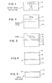
- FIGS. 1-5 illustrate an embodiment of the invention wherein the substrate is of silicon and the metal compound is a metal silicide formed by annealing overlying metal and silicon layers.
- the substrate 10 is either an n-doped single crystal silicon layer, or a p-doped single crystal silicon layer.
- the substrate could, of course, be intrinsic material.
- a layer 12 of n-doped polycrystalline silicon (or amorphous silicon) is deposited on the substrate 10. This can be done in any of several well known ways, including low temperature chemical vapour deposition or ion implantation into only the layer 12.
- the n-type dopants in the polysilicon layer 12 can include, for instance, As, Sb and P, all of which are well known n-type dopants. If p-type doping were required, a dopant such as B would be used.
- an overlying metal layer 14 is deposited on the polysilicon layer 12.
- the metal comprising layer 14 is preferably a noble or near-noble metal.
- Suitable metals include Pt, Pd, Ni, Ir, and Rh.
- FIG. 3 illustrates an annealing step in which the polysilicon layer 12 and metal layer 14 chemically combine to form a silicide layer 16. This consumes the layers 12 and 14, and produces an interface 18 which moves towards the substrate.
- the annealing step is performed at temperatures just sufficiently high to promote the growth of the metal silicide in order to snowplow dopants 20 originally in the polysilicon layer 12.
- the dopants can be in the metal layer 14 instead of in the polysilicon layer 12, or can be present in both layers 12 and 14.
- Annealing can be accomplished by any means including, for example, heating furnaces, flashlamps, and lasers.
- the important feature is that a metallic compound is formed, which is most easily achieved by an annealing (ie heating) step. Any low temperature step which forms a metallic compound with a moving interface could be used.
- Doping of these layers 12, 14 can be accomplished by chemical vapour deposition of dopant-containing gaseous species together with silicon-containing gaseous species, or by physical vapour deposition (evaporation or sputtering) of dopant and silicon species, or by a combination of chemical and physical vapour deposition.
- Doping of these layers 12, 14 can also be accomplished by ion implantation during or after deposition. This has the advantage that the dopants can be introduced at a desired depth in the polysilicon layer 12. By implanting near to the single crystal silicon interface (but entirely within the polysilicon layer 12), one can reduce the thickness of the polysilicon and metal layers, the resulting silicide layer, and the annealing time required for silicide formation and snowplow. Implantation gives good control of the doping level. Finally, because the implantation is only into the polysilicon layer 12, no implantation damage is created in the single crystal silicon I0; consequently, no high temperature annealing steps are needed, so the process remains a true low temperature doping technique.
- FIG. 4 illustrates the continuation of the annealing step in which the metal layer 14 still remains, but the polysilicon layer 12 has been entirely consumed by the formation of the metal silicide 16. If the annealing is sufficient and the initial thicknesses of the layers 12 and 14 are chosen properly, the compound forming interface 18 will advance entirely through the polysilicon layer 12 and into the silicon substrate 10, producing a new silicide/silicon interface located a small distance inside the original single-crystal silicon substrate 10. When this occurs, a considerable portion of the dopants originally introduced into the polysilicon layer 12 will have been snowplowed ahead of the advancing silicide/silicon interface to form a doped region 22 in the substrate 10.
- the depth of the doped region 22 into the top surface of the substrate 10 is less than a few hundred angstroms, ie a few tens of nanometers, and is typically about 30nm, or less.
- the doping concentration in region 22 depends on the initial doping level of substrate 10 and the amount of dopant present in the overlayer 12.
- the conductivity-type of the region 22 can be the same as that of the substrate 10, or opposite. Thus, a contact or a p-n junction can be created. For example, it is possible to dope the region 22 heavily (to an amount greater than 10 20 carriers/cm 3 ) to create an ohmic contact. Varying degrees of dopant concentration can be produced in the shallow doped region 22, to provide rectifying contacts, Schottky barriers, etc.
- the metal 14 and silicide layer 16 are not chemically removed, they can be used as device contacts whose electrical properties can be chosen.
- the metal 14 and silicide layer 16 can be used as device contacts whose electrical properties can be chosen.
- the polysilicon layer 12 can be delineated prior to the metal deposition in order to obtain a self-aligned Ohmic contact or p-n junction.
- the silicide overlayer 16 which has a low resistivity, can be patterned to form part of the interconnect metallization.
- the remaining metal 14 and compound 16 may be chemically removed from the surface of the single crystal silicon substrate 10, leaving the very thin doped region 22 at the surface of the substrate 10.
- Other processing steps including the process described here as well as other semiconductor device processes, can subsequently be employed to fabricate further device layers and structures, such as transistors and multilayer and superlattice devices.
- FIGS. 1-5 two layers 12, 14 were used to produce the metal silicide whose moving interface snowplowed dopants into the substrate.
- more than two layers (materials) can be used to produce the metal compound, and the compound need not be a silicide.
- Noble and near-noble metal silicides are advantageous, however, as these compounds can be formed at very low temperatures, and will have a sufficient snowplow effect to provide efficient doping of the substrate.
- these compounds can be used to reduce the resistance of polysilicon lines, and for interconnects and contacts, as will be seen with respect to FIGS. 6 and 7.
- the technique illustrated in FIGS. 1-5 will work with silicon substrates 10 of different crystallographic structures, such as (111) and (100).
- the snowplow effect can be used to introduce dopants into the top surface of the substrate 10 to a controlled, shallow depth.
- the snowplow effect can be used to drive the dopants past these imperfections and impurities into the body of the substrate. In this manner, a very shallow doped region of high integrity and uniformity can be formed at a desired depth in the substrate 10.
- Metal layer 14 is of a minimum thickness to insure that the entire thickness of layer 12 is consumed during metal compound formation.
- the thickness of metal layer 14 is greater than that required to consume all of layer 12, and also to insure that the growing interface extends into the substrate 10. As was noted, this insures that the dopants are snowplowed past any slight impurities or imperfections that would exist at the surface of the substrate in order to create the shallow doped region in the body of the substrate. Of course, if the top surface of the substrate is adequate, the silicide boundary can be made to stop at the beginning of the substrate, if desired (such as to prevent any consumption of the single crystal silicon substrate 10).
- the thicknesses of the layers 12 and 14 are initially determined with respect to the silicide phase which will be formed, in order to have the silicide interface extend the desired amount into the substrate 10.
- the annealing conditions (temperature, time) are then set to determine where the moving interface will stop. If metal layer 14 is entirely consumed, the fact that the annealing continues will not alter the depth of the silicide interface. Thus, an initial determination of the proper thicknesses of layers 12 and 14 provides a good control over the final location of the silicide interface.
- the amount of doping in the overlayers, and their thicknesses can be used to determine the amount of dopant introduced into the substrate.
- the doping in the polysilicon layer 12 will be about 2 x 10 18 carriers/cm 3 .
- This doping level can be produced in a 50nm thick layer 12 by CVD doping or by implanting at a dosage of 1013/cmz.
- the snowplow effect can be used to increase the doping level of the substrate by several orders of magnitude, or to initially dope intrinsic material. If the substrate is initially doped, it can be doped de- generately in a shallow region by the snowplow effect. Also, if the dopant level in the polysilicon layer 12 is increased to greater that 10 20 carriers/cm 3 , then a doping level of greater that 10 can be produced in the substrate. Generally, the polysilicon layer 12 is about 30nm thick, and can be, for example, 10-50nm thick. Thus, the dopant level in layer 12 can be changed to smoothly change the dopant concentration of shallow region 22, to any desired amount.
- metal silicides are not the only metallic compounds which can be formed at very low temperatures and which will exhibit a snowplow effect.
- the metal layer 14 may be combined with a doped Ge layer 12 to form germanide compounds 16.
- the metal layer 14 may be reacted with compound semiconductors (III-V or II-VI) to form new compounds combining metal and semiconductor constituents.
- layer 12 can be GaAs while metal layer 14 is Pd.
- Pd a metallic compound of Pd and Ga
- the chemistry of Pd on GaAs is described in more detail by P Oelhafen et al in J. Vac. Sci. Technol.
- Pt is another suitable metal that can be used for layer 14 when layer 12 is GaAs.
- the chemistry of Pt and GaAs is described by C Fontaine et al in Appl. Phys. 54, (3), page 1404, March 1983. When these materials are used, it is possible to free As from the GaAs layer, where the freed As would be snowplowed into the substrate 10.
- the dopants which are to be snowplowed into the substrate can be present as dopants in either or both of the layers 12 and 14, or can be a primary constituent of the material comprising one of these layers (such as As which is stoichiometrically joined with Ga to form GaAs).
- a layer (such as polysilicon or amorphous silicon layer 12) is provided which is consumed during the metal compound-forming step. This is important to move the interface of the metal compound close to or into the top surface of the substrate 10, and to prevent too much of the substrate 10 from being consumed. For example, if layer 12 were not used and a metal layer were deposited directly onto the silicon substrate 10, annealing would cause a reaction between the metal layer and the silicon substrate, and would consume a large amount of the substrate (comparable to the metal layer 14 thickness during the introduction of dopants into the substrate). This is undesirable, and is one of the problems noted with respect to reference 8.
- metal silicides are particularly good metal compounds to be used in the practice of this invention, not all metal silicides will work.
- Noble metal and near-noble metal silicides appear to work well and form compounds at low temperatures.
- refractory metal silicides require higher temperatures of formation, and do not exhibit significant snowplow effects (see reference 5). Even though the solubility of the same dopant in these different types of silicides may be similar, the refractory metal silicides do not snowplow dopants to the extent that the noble metal and near-noble metal silicides do. This may be explained somewhat by the mechanisms covering the growth of metal silicides, as is described in the aforementioned reference 5.
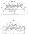
- FIGS. 6 and 7 show general diagrams of two devices in the production of which the process of the present invention has been used. While the buried collector transistor structure of FIG. 6 and the field effect device of FIG. 7 are chosen as representative examples, it will be appreciated that the present invention could be used to make other structures and devices.
- base, emitter, and collector contacts (B, E, and C, respectively) are shown which are comprised of a metal such as Al-Cu.
- a layer 24 of Ti-W is used as a diffusion barrier.
- the collector region is comprised of the n buried layer 26 which is a contact to an n region 27 while the emitter is comprised of an n region 28.
- the base is comprised of a p region 30, formed as a portion of the p-type region 32. Insulating regions 34 provide electrical isolation between adjacent devices, and between the emitter, base and collector contacts.
- the substrate is a p-type silicon wafer 35.
- PtSi regions 36 are used to make contact to the underlying doped regions of this device.
- these PtSi compounds can be used to snowplow dopants in order to form low resistivity contacts to region 28 and a shallow doped region 30.
- FIG. 7 shows a field effect transistor comprising a source contact S, a gate contact G, and a drain contact D.
- Insulating regions 38 such as SiO 2 , are located between adjacent devices, between adjacent metal contacts, and beneath the gate contact G.
- Metal silicide contacts 40 designated M Si, make electrical contact to the source and drain n regions 42.
- the substrate 44 is p-silicon.
- This invention can be used to make shallow n regions 42 beneath the metal silicide 40.
- regions 42 can be n-type, but of a lesser dopant concentration than the portions of these regions immediately below the silicide 40.
- n-dopants will be snowplowed into the top surface of regions 42, in order to produce n doping. In this way, an ohmic contact can be provided between the metal silicide layer 40 and the snowplowed doped region immediately below it.
- suitable metal silicides for use in this invention include silicides of metals of the transition series, and rare earth metal silicides.
- Noble and near-noble metals such as Pt, Pd, Ir, Rh, Os, Ru, and Ni may be preferred, since they form compounds such as silicides at low temperatures.
- Pt and Pd will form silicides at approximately 250°C, while most refractory metals form silicides at higher temperatures (500-700°C).
- the noble and near-noble silicides exhibit a stronger snowplow effect than do the refractory metal silicides.
- Refractory metals such as Cr and Ti, may be suitable.
- Rare earth metals can also be used, such as Er and Sm.
- overlayer 12 can be comprised of a III-V material other than GaAs, such as InP.
- suitable materials for overlayer 12 include II-VI materials such as CdTe and ZnSe. Suitable metal layers with these III-V and II-VI materials are, for example, Pt and Pd.
- the dopant can be present as a dopant in an overlayer (such as p in polysilicon) or can be a primary constituent of the overlayer (such as As in GaAs).
- the element to be used to dope the substrate can also be present as a dopant in a III-V or II-VI material, such as a Zn dopant in GaAs. During metal compound formation between the metal and/or Ga and As, the Zn would be released and pushed into the substrate.
- This technique can be used to dope a substrate with any kind of dopant, or dopants to produce different types of devices, including light emitting diodes.
Landscapes
- Engineering & Computer Science (AREA)
- Physics & Mathematics (AREA)
- Condensed Matter Physics & Semiconductors (AREA)
- General Physics & Mathematics (AREA)
- Manufacturing & Machinery (AREA)
- Computer Hardware Design (AREA)
- Microelectronics & Electronic Packaging (AREA)
- Power Engineering (AREA)
- Electrodes Of Semiconductors (AREA)
- Insulated Gate Type Field-Effect Transistor (AREA)
- Recrystallisation Techniques (AREA)
Applications Claiming Priority (2)
| Application Number | Priority Date | Filing Date | Title |
|---|---|---|---|
| US62294984A | 1984-06-21 | 1984-06-21 | |
| US622949 | 1984-06-21 |
Publications (2)
| Publication Number | Publication Date |
|---|---|
| EP0165547A2 true EP0165547A2 (de) | 1985-12-27 |
| EP0165547A3 EP0165547A3 (de) | 1987-08-26 |
Family
ID=24496165
Family Applications (1)
| Application Number | Title | Priority Date | Filing Date |
|---|---|---|---|
| EP85107228A Withdrawn EP0165547A3 (de) | 1984-06-21 | 1985-06-13 | Verfahren zum Erzeugen eines flach dotierten Gebietes ein einem Halbleitersubstrat |
Country Status (2)
| Country | Link |
|---|---|
| EP (1) | EP0165547A3 (de) |
| JP (1) | JPS618916A (de) |
Cited By (4)
| Publication number | Priority date | Publication date | Assignee | Title |
|---|---|---|---|---|
| EP0361078A3 (de) * | 1988-09-28 | 1990-04-25 | Fujitsu Limited | Verfahren zur Herstellung einer Halbleiter-Anordnung mit niedrigen hoch-dotierten Gebieten |
| GB2236119A (en) * | 1989-09-21 | 1991-03-27 | Int Rectifier Corp | Platinum diffusion process |
| WO1995006328A1 (en) * | 1993-08-27 | 1995-03-02 | National Semiconductor Corporation | Self-aligned cmos process |
| WO1995006327A1 (en) * | 1993-08-27 | 1995-03-02 | National Semiconductor Corporation | Bipolar transistor process |
Families Citing this family (6)
| Publication number | Priority date | Publication date | Assignee | Title |
|---|---|---|---|---|
| JPS6422026A (en) * | 1987-07-17 | 1989-01-25 | Sony Corp | Manufacture of semiconductor device |
| JPH01220824A (ja) * | 1988-02-29 | 1989-09-04 | Toshiba Corp | 半導体装置の製造方法 |
| JPH0235720A (ja) * | 1988-07-26 | 1990-02-06 | Matsushita Electric Ind Co Ltd | Mos型半導体装置の製造方法 |
| BE1015721A3 (nl) * | 2003-10-17 | 2005-07-05 | Imec Inter Uni Micro Electr | Werkwijze voor het reduceren van de contactweerstand van de aansluitgebieden van een halfgeleiderinrichting. |
| SG175752A1 (en) * | 2009-04-21 | 2011-12-29 | Tetrasun Inc | High-efficiency solar cell structures and methods of manufacture |
| EP2461352B1 (de) * | 2010-12-06 | 2013-07-10 | Imec | Verfahren zur Herstellung von Kontakten mit geringem Widerstand auf n-Germanium |
Family Cites Families (3)
| Publication number | Priority date | Publication date | Assignee | Title |
|---|---|---|---|---|
| US3869322A (en) * | 1973-10-15 | 1975-03-04 | Ibm | Automatic P-N junction formation during growth of a heterojunction |
| WO1983003029A1 (en) * | 1982-02-26 | 1983-09-01 | Western Electric Co | Diffusion of shallow regions |
| CA1198226A (en) * | 1982-06-01 | 1985-12-17 | Eliezer Kinsbron | Method for manufacturing a semiconductor device |
-
1985
- 1985-03-29 JP JP6402285A patent/JPS618916A/ja active Granted
- 1985-06-13 EP EP85107228A patent/EP0165547A3/de not_active Withdrawn
Cited By (9)
| Publication number | Priority date | Publication date | Assignee | Title |
|---|---|---|---|---|
| EP0361078A3 (de) * | 1988-09-28 | 1990-04-25 | Fujitsu Limited | Verfahren zur Herstellung einer Halbleiter-Anordnung mit niedrigen hoch-dotierten Gebieten |
| GB2236119A (en) * | 1989-09-21 | 1991-03-27 | Int Rectifier Corp | Platinum diffusion process |
| DE4029826A1 (de) * | 1989-09-21 | 1991-04-04 | Int Rectifier Corp | Platindiffusionsverfahren fuer einen halbleiterkoerper |
| GB2236119B (en) * | 1989-09-21 | 1994-05-25 | Int Rectifier Corp | Platinum diffusion process |
| AT398014B (de) * | 1989-09-21 | 1994-08-25 | Int Rectifier Corp | Verfahren zur diffundierung von die lebensdauer der minoritätsträger verringernden platinatomen |
| WO1995006328A1 (en) * | 1993-08-27 | 1995-03-02 | National Semiconductor Corporation | Self-aligned cmos process |
| WO1995006327A1 (en) * | 1993-08-27 | 1995-03-02 | National Semiconductor Corporation | Bipolar transistor process |
| US5453389A (en) * | 1993-08-27 | 1995-09-26 | National Semiconductor, Inc. | Defect-free bipolar process |
| US5571744A (en) * | 1993-08-27 | 1996-11-05 | National Semiconductor Corporation | Defect free CMOS process |
Also Published As
| Publication number | Publication date |
|---|---|
| JPS618916A (ja) | 1986-01-16 |
| JPH0311089B2 (de) | 1991-02-15 |
| EP0165547A3 (de) | 1987-08-26 |
Similar Documents
| Publication | Publication Date | Title |
|---|---|---|
| US4692348A (en) | Low temperature shallow doping technique | |
| US5656514A (en) | Method for making heterojunction bipolar transistor with self-aligned retrograde emitter profile | |
| US4717681A (en) | Method of making a heterojunction bipolar transistor with SIPOS | |
| EP0175864B1 (de) | Selbstausrichtender Feldeffekttransistor mit einem Metall-Halbleiter-Kontakt | |
| US5217923A (en) | Method of fabricating a semiconductor device having silicided source/drain regions | |
| US5563448A (en) | Ohmic contact structure of a highly integrated semiconductor device having two resistance control layers formed between a metal electrode and the substrate | |
| US4855246A (en) | Fabrication of a gaas short channel lightly doped drain mesfet | |
| EP0110211A2 (de) | Integrierte Schaltung mit bipolaren Transistoren und Verfahren zu ihrer Herstellung | |
| US4573064A (en) | GaAs/GaAlAs Heterojunction bipolar integrated circuit devices | |
| US6329277B1 (en) | Method of forming cobalt silicide | |
| US4593457A (en) | Method for making gallium arsenide NPN transistor with self-aligned base enhancement to emitter region and metal contact | |
| WO1985002714A1 (en) | Method of making a bipolar junction transistor | |
| EP0715769B1 (de) | Selbstausgerichtetes cmos-verfahren | |
| US4593307A (en) | High temperature stable ohmic contact to gallium arsenide | |
| US5089428A (en) | Method for forming a germanium layer and a heterojunction bipolar transistor | |
| EP0165547A2 (de) | Verfahren zum Erzeugen eines flach dotierten Gebietes ein einem Halbleitersubstrat | |
| EP0051534B1 (de) | Selbstjustierendes Verfahren zur Herstellung integrierter Stromkreisstrukturen unter Verwendung unterschiedlicher Oxydationsraten | |
| US4714685A (en) | Method of fabricating self-aligned silicon-on-insulator like devices | |
| JPH05347313A (ja) | 高速半導体デバイスの極薄活性領域の製造方法 | |
| US6064077A (en) | Integrated circuit transistor | |
| JP2664051B2 (ja) | 障壁の高さを高くする方法とシヨツトキー障壁 | |
| JPH0241170B2 (de) | ||
| US4408388A (en) | Method for manufacturing a bipolar integrated circuit device with a self-alignment base contact | |
| EP0200059B1 (de) | Verfahren zur Herstellung eines ohmischen Kontaktes auf einem III-V Halbleiter und hergestelltes Halbleiterzwischenprodukt | |
| US4804635A (en) | Method of manufacture of galluim arsenide field effect transistors |
Legal Events
| Date | Code | Title | Description |
|---|---|---|---|
| PUAI | Public reference made under article 153(3) epc to a published international application that has entered the european phase |
Free format text: ORIGINAL CODE: 0009012 |
|
| AK | Designated contracting states |
Designated state(s): DE FR GB |
|
| 17P | Request for examination filed |
Effective date: 19860424 |
|
| PUAL | Search report despatched |
Free format text: ORIGINAL CODE: 0009013 |
|
| AK | Designated contracting states |
Kind code of ref document: A3 Designated state(s): DE FR GB |
|
| 17Q | First examination report despatched |
Effective date: 19880622 |
|
| STAA | Information on the status of an ep patent application or granted ep patent |
Free format text: STATUS: THE APPLICATION HAS BEEN WITHDRAWN |
|
| 18W | Application withdrawn |
Withdrawal date: 19890217 |
|
| RIN1 | Information on inventor provided before grant (corrected) |
Inventor name: RUBLOFF, GARY WAYNE Inventor name: WITTMER, MARC FRANCIS |