EP0164867A2 - Durch Feldeffekt gesteuerte integrierte Thyristorstruktur mit geerdeter Kathode - Google Patents
Durch Feldeffekt gesteuerte integrierte Thyristorstruktur mit geerdeter Kathode Download PDFInfo
- Publication number
- EP0164867A2 EP0164867A2 EP85303115A EP85303115A EP0164867A2 EP 0164867 A2 EP0164867 A2 EP 0164867A2 EP 85303115 A EP85303115 A EP 85303115A EP 85303115 A EP85303115 A EP 85303115A EP 0164867 A2 EP0164867 A2 EP 0164867A2
- Authority
- EP
- European Patent Office
- Prior art keywords
- region
- type
- thyristor
- turn
- transistor
- Prior art date
- Legal status (The legal status is an assumption and is not a legal conclusion. Google has not performed a legal analysis and makes no representation as to the accuracy of the status listed.)
- Withdrawn
Links
- 230000000694 effects Effects 0.000 claims abstract description 12
- 239000004065 semiconductor Substances 0.000 claims abstract description 8
- 230000008859 change Effects 0.000 claims abstract description 3
- 230000005669 field effect Effects 0.000 claims description 23
- 230000001172 regenerating effect Effects 0.000 claims description 7
- 108091006146 Channels Proteins 0.000 claims description 5
- 102000004129 N-Type Calcium Channels Human genes 0.000 claims description 4
- 108090000699 N-Type Calcium Channels Proteins 0.000 claims description 4
- 230000009977 dual effect Effects 0.000 claims description 4
- 229910052710 silicon Inorganic materials 0.000 description 9
- 239000010703 silicon Substances 0.000 description 9
- XUIMIQQOPSSXEZ-UHFFFAOYSA-N Silicon Chemical compound [Si] XUIMIQQOPSSXEZ-UHFFFAOYSA-N 0.000 description 8
- 229910021420 polycrystalline silicon Inorganic materials 0.000 description 7
- VYPSYNLAJGMNEJ-UHFFFAOYSA-N Silicium dioxide Chemical compound O=[Si]=O VYPSYNLAJGMNEJ-UHFFFAOYSA-N 0.000 description 6
- 239000011248 coating agent Substances 0.000 description 5
- 238000000576 coating method Methods 0.000 description 5
- 238000002347 injection Methods 0.000 description 5
- 239000007924 injection Substances 0.000 description 5
- 239000002184 metal Substances 0.000 description 4
- 230000008901 benefit Effects 0.000 description 3
- 230000000903 blocking effect Effects 0.000 description 3
- 239000012535 impurity Substances 0.000 description 3
- 235000012239 silicon dioxide Nutrition 0.000 description 3
- 239000000377 silicon dioxide Substances 0.000 description 3
- 239000005360 phosphosilicate glass Substances 0.000 description 2
- 230000009471 action Effects 0.000 description 1
- 238000013459 approach Methods 0.000 description 1
- 210000000746 body region Anatomy 0.000 description 1
- 239000000969 carrier Substances 0.000 description 1
- 230000015556 catabolic process Effects 0.000 description 1
- 230000001939 inductive effect Effects 0.000 description 1
- 238000000034 method Methods 0.000 description 1
- 230000004048 modification Effects 0.000 description 1
- 238000012986 modification Methods 0.000 description 1
- 238000004806 packaging method and process Methods 0.000 description 1
- 239000013641 positive control Substances 0.000 description 1
- 230000008569 process Effects 0.000 description 1
- 230000000630 rising effect Effects 0.000 description 1
Images
Classifications
-
- H—ELECTRICITY
- H01—ELECTRIC ELEMENTS
- H01L—SEMICONDUCTOR DEVICES NOT COVERED BY CLASS H10
- H01L29/00—Semiconductor devices specially adapted for rectifying, amplifying, oscillating or switching and having potential barriers; Capacitors or resistors having potential barriers, e.g. a PN-junction depletion layer or carrier concentration layer; Details of semiconductor bodies or of electrodes thereof ; Multistep manufacturing processes therefor
- H01L29/66—Types of semiconductor device ; Multistep manufacturing processes therefor
- H01L29/68—Types of semiconductor device ; Multistep manufacturing processes therefor controllable by only the electric current supplied, or only the electric potential applied, to an electrode which does not carry the current to be rectified, amplified or switched
- H01L29/70—Bipolar devices
- H01L29/74—Thyristor-type devices, e.g. having four-zone regenerative action
- H01L29/744—Gate-turn-off devices
- H01L29/745—Gate-turn-off devices with turn-off by field effect
-
- H—ELECTRICITY
- H01—ELECTRIC ELEMENTS
- H01L—SEMICONDUCTOR DEVICES NOT COVERED BY CLASS H10
- H01L29/00—Semiconductor devices specially adapted for rectifying, amplifying, oscillating or switching and having potential barriers; Capacitors or resistors having potential barriers, e.g. a PN-junction depletion layer or carrier concentration layer; Details of semiconductor bodies or of electrodes thereof ; Multistep manufacturing processes therefor
- H01L29/02—Semiconductor bodies ; Multistep manufacturing processes therefor
- H01L29/06—Semiconductor bodies ; Multistep manufacturing processes therefor characterised by their shape; characterised by the shapes, relative sizes, or dispositions of the semiconductor regions ; characterised by the concentration or distribution of impurities within semiconductor regions
- H01L29/0684—Semiconductor bodies ; Multistep manufacturing processes therefor characterised by their shape; characterised by the shapes, relative sizes, or dispositions of the semiconductor regions ; characterised by the concentration or distribution of impurities within semiconductor regions characterised by the shape, relative sizes or dispositions of the semiconductor regions or junctions between the regions
-
- H—ELECTRICITY
- H01—ELECTRIC ELEMENTS
- H01L—SEMICONDUCTOR DEVICES NOT COVERED BY CLASS H10
- H01L29/00—Semiconductor devices specially adapted for rectifying, amplifying, oscillating or switching and having potential barriers; Capacitors or resistors having potential barriers, e.g. a PN-junction depletion layer or carrier concentration layer; Details of semiconductor bodies or of electrodes thereof ; Multistep manufacturing processes therefor
- H01L29/02—Semiconductor bodies ; Multistep manufacturing processes therefor
- H01L29/06—Semiconductor bodies ; Multistep manufacturing processes therefor characterised by their shape; characterised by the shapes, relative sizes, or dispositions of the semiconductor regions ; characterised by the concentration or distribution of impurities within semiconductor regions
- H01L29/10—Semiconductor bodies ; Multistep manufacturing processes therefor characterised by their shape; characterised by the shapes, relative sizes, or dispositions of the semiconductor regions ; characterised by the concentration or distribution of impurities within semiconductor regions with semiconductor regions connected to an electrode not carrying current to be rectified, amplified or switched and such electrode being part of a semiconductor device which comprises three or more electrodes
- H01L29/1012—Base regions of thyristors
- H01L29/1016—Anode base regions of thyristors
-
- H—ELECTRICITY
- H01—ELECTRIC ELEMENTS
- H01L—SEMICONDUCTOR DEVICES NOT COVERED BY CLASS H10
- H01L29/00—Semiconductor devices specially adapted for rectifying, amplifying, oscillating or switching and having potential barriers; Capacitors or resistors having potential barriers, e.g. a PN-junction depletion layer or carrier concentration layer; Details of semiconductor bodies or of electrodes thereof ; Multistep manufacturing processes therefor
- H01L29/40—Electrodes ; Multistep manufacturing processes therefor
- H01L29/41—Electrodes ; Multistep manufacturing processes therefor characterised by their shape, relative sizes or dispositions
- H01L29/423—Electrodes ; Multistep manufacturing processes therefor characterised by their shape, relative sizes or dispositions not carrying the current to be rectified, amplified or switched
- H01L29/42308—Gate electrodes for thyristors
-
- H—ELECTRICITY
- H01—ELECTRIC ELEMENTS
- H01L—SEMICONDUCTOR DEVICES NOT COVERED BY CLASS H10
- H01L29/00—Semiconductor devices specially adapted for rectifying, amplifying, oscillating or switching and having potential barriers; Capacitors or resistors having potential barriers, e.g. a PN-junction depletion layer or carrier concentration layer; Details of semiconductor bodies or of electrodes thereof ; Multistep manufacturing processes therefor
- H01L29/66—Types of semiconductor device ; Multistep manufacturing processes therefor
- H01L29/68—Types of semiconductor device ; Multistep manufacturing processes therefor controllable by only the electric current supplied, or only the electric potential applied, to an electrode which does not carry the current to be rectified, amplified or switched
- H01L29/70—Bipolar devices
- H01L29/74—Thyristor-type devices, e.g. having four-zone regenerative action
- H01L29/744—Gate-turn-off devices
- H01L29/745—Gate-turn-off devices with turn-off by field effect
- H01L29/7455—Gate-turn-off devices with turn-off by field effect produced by an insulated gate structure
-
- H—ELECTRICITY
- H01—ELECTRIC ELEMENTS
- H01L—SEMICONDUCTOR DEVICES NOT COVERED BY CLASS H10
- H01L29/00—Semiconductor devices specially adapted for rectifying, amplifying, oscillating or switching and having potential barriers; Capacitors or resistors having potential barriers, e.g. a PN-junction depletion layer or carrier concentration layer; Details of semiconductor bodies or of electrodes thereof ; Multistep manufacturing processes therefor
- H01L29/66—Types of semiconductor device ; Multistep manufacturing processes therefor
- H01L29/68—Types of semiconductor device ; Multistep manufacturing processes therefor controllable by only the electric current supplied, or only the electric potential applied, to an electrode which does not carry the current to be rectified, amplified or switched
- H01L29/70—Bipolar devices
- H01L29/74—Thyristor-type devices, e.g. having four-zone regenerative action
- H01L29/749—Thyristor-type devices, e.g. having four-zone regenerative action with turn-on by field effect
Definitions
- This invention relates to thyristor structures and more particularly to a dual gate silicon controlled rectifier in which one gate is used for device turn-on and the other gate is used for device turn-off.
- Numerous semiconductor devices can be used as power switches. These devices include thyristors, bipolar junction transistors, junction field effect transistors, insulated gate field effect transistors, field controlled thyristors, insulated gate controlled thyristors, and bipolar mode conductivity modulated field effect transistors.
- the choice of which device is preferred for a particular application is a function of many factors. These factors include the desired current handling capability of the device, the forward and reverse blocking voltages desired, turn-on and turn-off time desired, typical and maximum switching frequencies desired, circuit environment considerations such as resistive/inductive loads encountered, drive requirements, cost, etc.
- thyristor devices used for automotive switching applications.
- Such characteristics include a grounded cathode for compatibility with the automotive electrical system and control by means of low current and low positive voltages. This provides simpler interfacing and better electrical compatibility with other circuits in the automotive system.
- the thyristor not only be rapidly turned on, but also rapidly turned off, by the low power positive control voltages.
- Low cost is very important too.
- a high current density device with a low on-resistance is desired. This minimizes silicon chip area in the device and thereby improves yields, while keeping heat sinking and packaging costs to a minimum.
- this invention provides a dual gate thyristor in which a turn-on gate is part of a first integrated insulated gate field effect transistor (IGFET) and a turn-offgate is part of a second integrated insulated gate field effect transistor (IGFET).
- the thyristor further includes a pinch resistance effect for accelerating turn-off, which effect is produced by a ring-like source region of the second IGFET that encircles an internal region of the thyristor.
- This invention also provides a new semiconductor power device suitable for electrical switching in automotive applications.
- This invention further provides a semiconductor power device having low specific on-resistance characteristic of bipolar regenerative switching devices, in combination with the convenience of insulated gate control of both turn-on and turn-off.
- This invention comprehends a PNPN rectifier structure that has a grounded cathode and two insulated control gates, one for turn-on and one for turn-off.
- the rectifier is referred to as a thyristor since it is fundamentally a bipolar type of device that uses conductivity modulation to handle high current densities and provide a low specific on-resistance.
- the control gates are actually gate electrodes of separate integral insulated gate field effect transistors (IGFETs) and controlled with positive electrical potentials.
- the thyristor structure provides a pinch resistance, analogous in operation to a junction field effect transistor that is activated by the turn-off control gate.
- insulated gates have been used to turn-on thyristors.
- thyristors can only be turned off when current density drops to a low value.
- the thyristor of this invention additionally has a second insulated gate and a pinch resistance to provide turn-off even though current density does not decrease.
- the extra complexity introduced into the structure by using two control terminals and the pinch resistance is not considered to be significant when considering the advantage obtained, particularly for microprocessor controlled applications.
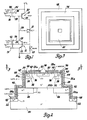
- FIG. 1 shows an electrical schematic that represents the integrated electrical devices inherent to the thyristor of this invention.
- This thyristor can thus be considered as including a PNP transistor 10, an NPN transistor 12, a first insulated gate field effect transistor (IGFET) 14, and a second insulated gate field effect transistor (IGFET) 16. It also includes a pinch resistance, referred to as a junction field effect transistor (JFET) 18.
- Figure 1 also shows a resistance 20, that is identified as Rshunt' Resistance 20 is an internal resistance, between the emitter and the base of the NPN transistor, that is used in the normal and accepted way to produce device turn-on when IGFET 14 is activated.
- Rshunt' Resistance 20 is an internal resistance, between the emitter and the base of the NPN transistor, that is used in the normal and accepted way to produce device turn-on when IGFET 14 is activated.
- Figure 2 shows a specific embodiment of the thyristor electrically represented by Figure 1.
- the structure shown in Figure 2 is fundamentally concentric. Hence, it is symmetrical about its vertical centreline.
- Figure 2 shows a rectangular P - silicon body member 24 that is symmetrical about its centre line and includes two circumferential steps, i.e. reduced cross-section zones, on its edge.
- the tread-portion of the lowest step on silicon body 24 has a ring-like N + region 22 on its circumference.
- the tread-portion of the middle step on the P - body 24, has a middle ring-like N + region 26.
- the middle N + ring 26 is disposed on the periphery of the upper surface of P body, so that it encircles a portion 24b of body 24 on the upper surface of body 24.
- a spacing between the lower N + ring 22 and the middle N + ring 26 should be maintained to insure that there is adequate shunt resistance 20 between junction J2 and cathode 22.
- this spacing should be at least of the order of 10 micrometers, preferably 30.
- N - epitaxial layer 28 of the order of about 500 - 1000 micrometers wide and about 20 - 50 micrometers thick is disposed on the upper surface of the P - body 24, over its central portion 24b and overlapping onto the inner circumferential portion of the middle N region 26.
- N - layer 28 could have a doping level of about 1 x 10 14 or 1 x 10 15 impurity atoms per cubic centimeter.
- the preferred width of layer 28 depends on the current capability desired for the device and the bonding wire diameter that is to be used.
- the preferred thickness of layer 28 depends upon the voltage breakdown. The range in width and thickness given is intended for a 5 ampere, 100 volt device.
- An island-like P region 30 is centrally disposed on the upper surface of the N - epitaxial layer 28.
- the P + and N + doping levels can be about 1 x 10 19 to 1 x 10 20 impurity atoms per cubic centimeter in this device.
- the lower N + ring 22 forms a PN junction, identified as J l, with the P - body portion 24.
- the P - body portion 24 forms a second PN junction, identified as J2, with the middle N + ring 26 and the N - epitaxial layer 28.
- the epitaxial layer 28 forms a third PN junction, identified as J3, with the island-like region 30.
- Junctions Jl and J2 comprise the NPN transistor 12.
- Junctions J2 and J3 comprise the PNP transistor 10.
- the lower N + ring 22 is an emitter region for the NPN transistor 12, while the P + region 30 is the emitter region for the PNP transistor 10.
- the P - body portion 24 can be considered as being both the base region of the NPN transistor and the collector region of the PNP transistor.
- the middle N ring 26 and its contiguous N - epitaxial layer 28 can be considered as being both the collector region of the N P N transistor 12 and the base region of the PNP transistor 10.
- the upper surface of the epitaxial layer 28 has a circumferential P-type ring 32 on its outer periphery, outwardly spaced from the P island 30. Accordingly, the P-type ring 32 forms a concentric ring around the P + island region 30, with a portion 28a of the epitaxial layer 28 between them.
- An N + circumferential ring 34 is nested wholly within the outer periphery of the P-type ring 32. It thus forms a third and upper N + ring, that is disposed on the top step of the device structure. This top step is the outer edge of the upper surface of the epitaxial layer 28.
- a PN junction 36 separates the P-type ring 32 from the epitaxial layer 28.
- a PN junction 38 separates the upper N + ring 34 from its surrounding P-type ring 32.
- a 1000 - 10,000 angstroms thick silicon dioxide film 40 of IGFET gate quality covers the top and sides of the epitaxial layer 28 and the silicon body 24.
- This silicon dioxide layer need not be uniform on the top and sides of the epitaxial layer 28 and the silicon body 24. On the sides of layer 28 and body 24 it can be thinner than on top of layer 28.
- the silicon dioxide film 40 is a dielectric that is suitable as a gate electrode dielectric for an insulated gate field effect transistor.
- a first circumferential polycrystalline silicon electrode 42 is disposed on the middle step and on the contiguous riser portion, i.e. side wall, of the body 24 beneath it. Thus, it extends from the N + lower ring 22 up to the N + middle ring 26.
- a second circumferential polycrystalline silicon electrode 44 is disposed on the middle and top steps and on the interjacent riser portion, i.e. side wall, of the epitaxial layer 28 therebetween. Thus, it extends from the N middle ring 26 to the upper N + ring 34.
- These polycrystalline silicon electrodes can be formed by a single polycrystalline silicon layer followed by a proper delineation process to separate the electrodes.
- a phosphosilicate glass coating 46 covers the dielectric coating 40 and the polycrystalline silicon electrodes 42 and 44.
- Windows in the dielectric coating 40 and the phosphosilicate glass coating 46 are provided so that a metal electrode 48, referred to herein as a cathode, can make contact with the N + ring 22 and optionally with the P - body 24 on the bottom step.
- Windows are also provided in the dielectric coating over the P island 30 and over its concentric upper N + ring 34, so that a metal electrode 50 can selectively make contact with both of the island and the ring.
- upper N + region 34 is electrically in parallel with the PNP emitter region 30 by means of the metal electrode 50.
- the metal electrode 50 is referred to herein as an anode. In operation, anode 50 is connected to a source of electrical potential that is positive with respect to the electrical potential applied to the cathode 48. In automotive applications, the cathode would be grounded together with the P - body 24.
- the IGFET used to turn-on the thyristor is indicated by reference numeral 14. It comprises the lowermost N + ring 22 as a source region, the middle N + ring 26 as a drain region, and the interjacent P - body portion 24a as a gate region.
- the IGFET used for turn-off of the device is formed by the middle N ring 26 and the side wall portion of the epitaxial layer 28 as a source region, the upper N + ring 34 as a drain region, and the interjacent portion 32a as a gate, i.e. channel, region.
- Polycrystalline silicon electrode 42 forms a gate electrode for turn-on IGFET 14. It thus forms a turn-on control gate for the thyristor.
- polycrystalline silicon electrode 44 forms a gate electrode for turn-off IGFET 16. It thus forms a turn-off control gate for the thyristor, with the P-type ring portion 32a as a gate region.
- the middle portion 24b on the upper surface of silicon body 24 projects upwardly into the centre of the middle circumferential N + ring 26. Hence, ring 26 completely encircles portion 24b. It should also be noted that the middle N + ring 26 has no electrical contact to it. It is allowed to electrically float in accordance with potentials applied to the gate electrodes 42 and 44. It should also be noted that the resistance R shunt' indicated by reference numeral 20 in Figure 1, is an internal resistance in the silicon body region 24 extending from portion 24b to the cathode contact 48.
- the shunt resistance 20 is of a value related to the characteristics of the turn-on IGFET that produces turn-on of the thyristor at a predetermined control gate voltage. While shunt resistance 20 should be considered here, it is no more important to this invention than it is to the prior single insulated gate controlled thyristors.
- the voltage drop across the shunt resistance 20 is sufficient to allow the forward bias of the N P N transistor 12 and emitter-base junction Jl.
- the current gain alpha of each of the two transistors increases as current increases. When the sum of the two alphas exceeds one, regenerative switching to a low voltage, high current state will take place, as is known. Accordingly, for turn-on, the thryristor is similar to the prior single insulated gate thyristors previously referred to. Commercially available versions of these are referred to as COMFETs and as IGTs. It is considered that turn-on operation and design principles are similar.
- the shunt resistance 20 is of a value, as compared to the conduction characteristics of the turn-on IGFET 14 to forward bias the base-emitter junction of the NPN transistor 12. Since shunt resistance 20 serves a turn-on purpose in this invention similar to what it does in the prior COMFET, the same prior considerations respecting its use should still be observed. This invention does not change them.
- Turn-off of this thyristor is obtained by means of the second IGFET 16.
- turn-off is produced by first turning off IGFET 14, if it was not previously turned off. This is accomplished, of course, by removing the positive potential that was previously applied to gate electrode 42, to turn-on the thyristor.
- Turn-off of the thyristor can then be accomplished by turning on IGFET 16.
- IGFET 16 is turned on by applying a positive electrical potential to the gate electrode 44, of the turn-off IGFET 16 that is above a channel threshold value. This produces an N-type channel 32a along the surface of the P-type outer ring 32 beneath the gate electrode 44.
- the N - type channel provides a low resistance electrical path between the epitaxial layer 28 and the upper N ring 34, which is in direct contact with anode 50.
- epitaxial layer 28 serves not only as the collector for the NPN transistor 12, but also as the base region for the P NP transistor 10.
- this low current path is electrically in parallel with the base-emitter junction J3 of the PNP transistor 10. Accordingly, the forward bias of the PNP transistor emitter-base junction J3 will be reduced, reducing hole injection across this junction. The attendant hole current flow through the PNP transistor 10 is thus reduced, reducing base drive to NPN transistor 12 that tends to turn it off.
- turn-off gate 44 does not just extend to the N - epitaxial layer 28. It extends completely across the edge of N - epitaxial layer onto the middle N + ring 26. Thus, the N - channel produced by a positive potential on gate 44 provides a low electrical resistance path between upper N + ring 34 and middle N + ring 26.
- the upper N + ring 34 is shorted to anode 50 and (b) the middle N + ring 26 electrically floats.
- the turn-off IGFET 16 is conducting, the electrical potential of the middle N ring 26 approaches that of anode 50.
- the resulting strong reverse bias on the junction J2 produces a space charge region that inhibits current flow through the centre portion 24b of the silicon body 24.
- the middle N ring 26 acts as a junction field effect transistor gate in pinching off the path for hole flow from anode 50 through the P region to cathode 48.
- the pinch resistor is shown as the junction field effect transistor (JFET) 18, in which its source and drain would be the top and bottom of P - region 24b, respectively.
- JFET junction field effect transistor
- the epitaxial layer is only lightly doped, the predominant hole flow will occur from the P + island 30 directly to the central P portion 24b aligned beneath it, rather than to the outlying portions of the P - body 24 beneath the middle N + ring 26.
- the positive potential is applied to the turn-off gate electrode 44, the resulting positive field on the side wall of epitaxial layer 28 tends to confine hole flow into the middle of the epitaxial layer 28.
- the emitter 30 of the PNP transistor be centrally located, that the epitaxial layer 28 be lightly doped, and that the P-type body 24 and the N-type epitaxial layer both be lightly doped.
- doping is normally inherent to a thyristor. Accordingly, the same type of doping relationships and levels can be used in this invention that would ordinarily be used in any other thyristor.
- the middle N + ring 26 should have an inner diameter that is small enough to completely pinch off current flow through the central P - portion 24b at the field effect produced on the portions 24b at the voltage and current flow at which turn-off is desired. That field effect would depend upon the voltage applied at anode 50, the conductivity of the turn-off IGFET 16, the conductivity of N + ring 26, current flow from anode to cathode, etc.
- the inner diameter of this thyristor is thus variable, depending on a plurality of factors. However, for automotive applications, it is preferred that the inner diameter of N + ring 26 be about 4 - 10 micrometers. This spacing is based on achieving the blocking capability of about 80 volts or higher on the anode.
- the inner diameter of the middle N + region 26 be larger than the outer diameter of the P + island region 30, at least by about 10 - 50 percent. This requirement can be eliminated or made less stringent if a mesh-like N + region 26 is used instead of a simple ring as mentioned earlier.
- the middle N + region not project beneath the epitaxial layer 28 significantly more than the most significant electron depletion effect produced by the positive potential applied to the turn-off gate electrode 44, in order to further prevent the middle N + region 26 from siphening off any significant proportion of the holes injected into the epitaxial region 28 from the PNP emitter region 30.
- the middle N + region 26 should not project beneath the epitaxial region 28 more than about 3 - 15 micrometers.
- a thyristor can be made conductive, i.e. start regenerative switching, by simply increasing the anode-cathode applied voltages. In this thyristor, such an effect can also occur.
- the pinch effect of the middle N + ring 26 shields the anode from the cathode. Consequently, this thyristor can withstand higher anode-cathode voltages if a positive voltage is applied to the turn-off gate electrode 44.
- a COMFET can turn-on simply because of a rapid voltage rise on the anode or if the temperature significantly increases. Such an effect can occur in this device too. However, this can be protected against by leaving a positive voltage on gate electrode 44.
- N + region 22 could have inner edge conformations to increase edge length, or be formed on the bottom side of P - body 24. Alternatively such regions could be used in addition to N + region 22 to increase the electron injection. These alternative or additional regions should be outside the central region, i.e. not directly below region 30, to prevent unintentional latching during turn-off or high temperature operation or when a rapidly rising anode voltage is applied.
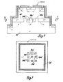
- the middle N + ring 26 is a different pattern.
- the middle N + ring 26 is a simple ring.
- the middle N + ring 26' also has a lattice arrangement in its centre. This lattice is formed by integral column extensions 26a' and integral row extensions 26b'. The intersecting rows and columns 26a' and 26b' leave a plurality of discrete portions 24b' of the body 24' therebetween.
- Each of these multiple discrete portions 24b' can form an individual pinch-resistance region in the resultant structure. Accordingly, a very large area device can be made that can have a considerable power rating.
- Each individual pinch-resistance region 24b' would then preferably have a width of about 4 - 10 micrometers, as was described in connection with portion 24b of Figures 2 - 3.
- N + middle layer 26' in Figures 4 and 5 need not be a lattice.
- rows 26a' may be chosen spaced 4 - 10 micrometers apart or columns 26b' spaced 4 - 10 micrometers apart.
- additional conformations on the inner periphery of the middle N + layer 26 provides additional emitter edge, which enhances electron injection efficiency for the NPN transistor. Accordingly, the unique configuration of the middle N layer not only enhances turn-off characteristics of the device but also should make it turn-on faster.
- This device has been shown as a vertical structure.
- an equivalent device could be made in a horizontal, i.e. lateral, structure.
- the lateral structure would appear in plan view quite similar to what is shown in cross section in Figure 2.
- the most distinctive characteristic would be that one end of the semiconductive film would be of one conductivity type, the other end would be of the opposite conductivity type with anode and cathode disposed at these opposite ends.
- the principal distinguishing feature would be that there would be an electrically floating middle N + region connected to turn-on and turn-off IGFETs, to provide a pinch resistance in accordance with this invention.
- Drain region 34 is electrically shorted to the anode 50 only to provide a convenient and simple source of positive potential for the drain region of the turn-off IGFET 16.
- a separate electrical contact may be provided to drain region 34 and connected it to a separate source of positive potential (also not shown), which may be referred to as V DD . If anode voltage is approximately 80 volts, a potential of only about 8 - 10 volts could be used on VDD . In such event, a voltage of about 4 or 5 volts need be used on the gate electrode 44 of the turn-off IGFET 16 in order to turn off the entire thyristor.
- drain 34 is electrically shorted to the anode 50 a considerably higher voltage may have to be applied to the gate electrode 44 in order to raise the voltage on N + region 26 sufficiently to get a rapid turn-off.
- a considerably higher voltage may have to be applied to the gate electrode 44 in order to raise the voltage on N + region 26 sufficiently to get a rapid turn-off.
- Use of such a high control voltage may not be desirable in some applications. Accordingly, it may be preferable to: have a separate electrical contact for the drain region 34.
- This invention involves an electrical pinch effect produced by an electrically floating N + region 26.
- the turn-off IGFET 16 is a means for applying a positive voltage to the N + region 26.
- Other IGFET structures and other means may be desired to bring up the desired positive potential for turn-off.
- the N + region 26 could be of any configuration which provides a pinch effect normal to the direction of current carrier flow in the device. This is irrespective of whether the device can be considered as a vertical cylindrical device or as a film (i.e. lateral) device. If it is to be made as a film device, an N + region can be provided extending from one edge of the film almost across to the other edge, or two opposed regions extending toward one another from opposite edges. In any event, a small portion of the film would be left forming the PNP collector region that would have a maximum dimension no greater than that which can be pinched off by the voltage being applied to the N + region, or regions, 26.
- the portion of the PNP transistor collector region normal to the direction of current carrier flow would not have a maximum dimension larger than that which could be substantially depleted of carriers by the positive voltage applied to the contiguous N + region 26. If a higher power device is desired, a multiplicity of such pinch regions can be used, such as is inherent to the lattice-type structure shown in connection with Figures 4 and 5.
- Another alternative resides in reversing the polarity of the anode and cathode and the conductivity type of the respective regions.
- the pinch region 26 would then be P , and a negative potential would be applied to it to cause the device to turn off.
- This variation is not practical for present automotive applications but might be of use in future or other applications.
Landscapes
- Engineering & Computer Science (AREA)
- Microelectronics & Electronic Packaging (AREA)
- Power Engineering (AREA)
- Physics & Mathematics (AREA)
- Ceramic Engineering (AREA)
- Condensed Matter Physics & Semiconductors (AREA)
- General Physics & Mathematics (AREA)
- Computer Hardware Design (AREA)
- Thyristors (AREA)
- Circuit Arrangements For Discharge Lamps (AREA)
- Electronic Switches (AREA)
Applications Claiming Priority (2)
| Application Number | Priority Date | Filing Date | Title |
|---|---|---|---|
| US617106 | 1984-06-04 | ||
| US06/617,106 US4611235A (en) | 1984-06-04 | 1984-06-04 | Thyristor with turn-off FET |
Publications (2)
| Publication Number | Publication Date |
|---|---|
| EP0164867A2 true EP0164867A2 (de) | 1985-12-18 |
| EP0164867A3 EP0164867A3 (de) | 1986-11-20 |
Family
ID=24472283
Family Applications (1)
| Application Number | Title | Priority Date | Filing Date |
|---|---|---|---|
| EP85303115A Withdrawn EP0164867A3 (de) | 1984-06-04 | 1985-05-02 | Durch Feldeffekt gesteuerte integrierte Thyristorstruktur mit geerdeter Kathode |
Country Status (4)
| Country | Link |
|---|---|
| US (1) | US4611235A (de) |
| EP (1) | EP0164867A3 (de) |
| JP (1) | JPS60263465A (de) |
| CA (1) | CA1225164A (de) |
Cited By (5)
| Publication number | Priority date | Publication date | Assignee | Title |
|---|---|---|---|---|
| DE3737790A1 (de) * | 1986-11-17 | 1988-05-26 | Gen Motors Corp | Quer-doppelgate-thyristor und verfahren zu seiner herstellung |
| DE3821459A1 (de) * | 1987-07-06 | 1989-01-19 | Gen Electric | Mit mos-gate abschaltbarer thyristor |
| EP0359994A1 (de) * | 1988-09-22 | 1990-03-28 | Asea Brown Boveri Ag | Steuerbares Leistungshalbleiterbauelement |
| GB2267996A (en) * | 1992-06-01 | 1993-12-22 | Fuji Electric Co Ltd | Dual gate mos thyristor |
| EP1371098A1 (de) * | 2001-03-02 | 2003-12-17 | University of Connecticut, Center for Science & Technology Com. | Thyristor- und komplementär-transistorkombination mit modulationsdotierung für eine monolithische optoelektronische integrierte schaltung |
Families Citing this family (11)
| Publication number | Priority date | Publication date | Assignee | Title |
|---|---|---|---|---|
| US4811072A (en) * | 1982-09-24 | 1989-03-07 | Risberg Robert L | Semiconductor device |
| GB2164790A (en) * | 1984-09-19 | 1986-03-26 | Philips Electronic Associated | Merged bipolar and field effect transistors |
| JPS624368A (ja) * | 1985-06-28 | 1987-01-10 | シ−メンス、アクチエンゲゼルシヤフト | サイリスタ |
| FR2595496B1 (fr) * | 1986-03-04 | 1988-05-06 | Labo Electronique Physique | Relais optique operant en mode d'accumulation de charges |
| JPS63141375A (ja) * | 1986-12-03 | 1988-06-13 | Fuji Electric Co Ltd | 絶縁ゲ−ト電界効果トランジスタ |
| US4861731A (en) * | 1988-02-02 | 1989-08-29 | General Motors Corporation | Method of fabricating a lateral dual gate thyristor |
| JPH0793425B2 (ja) * | 1992-04-07 | 1995-10-09 | 東洋電機製造株式会社 | プレーナ構造のmos制御サイリスタ |
| JP2801127B2 (ja) * | 1993-07-28 | 1998-09-21 | 日本碍子株式会社 | 半導体装置およびその製造方法 |
| DE19859502C2 (de) * | 1998-12-22 | 2000-12-07 | Siemens Ag | Sperrschicht-Feldeffekttransistor mit höher dotiertem Verbindungsgebiet |
| US20070114565A1 (en) * | 2005-11-23 | 2007-05-24 | Makaram Udaysimha A | Integrated field-effect transistor-thyristor device |
| CN110896102B (zh) * | 2019-11-04 | 2021-03-30 | 西安电子科技大学 | 一种基于双mos栅控的n型碳化硅晶闸管及其制备方法 |
Citations (3)
| Publication number | Priority date | Publication date | Assignee | Title |
|---|---|---|---|---|
| FR1433766A (fr) * | 1964-04-29 | 1966-04-01 | Siemens Ag | Soupape semiconductrice commandée avec amorçage par effet de champ |
| GB2040567A (en) * | 1979-01-29 | 1980-08-28 | Meidensha Electric Mfg Co Ltd | Gate controlled semiconductor device |
| FR2524710A1 (fr) * | 1982-04-01 | 1983-10-07 | Gen Electric | Dispositif de commutation a semi-conducteur |
Family Cites Families (3)
| Publication number | Priority date | Publication date | Assignee | Title |
|---|---|---|---|---|
| SU228793A1 (en) * | 1965-10-04 | 1980-01-05 | Fiz Tekh Inst Ioffe | Controlled valve |
| JPS5629458B2 (de) * | 1973-07-02 | 1981-07-08 | ||
| US5014102A (en) * | 1982-04-01 | 1991-05-07 | General Electric Company | MOSFET-gated bipolar transistors and thyristors with both turn-on and turn-off capability having single-polarity gate input signal |
-
1984
- 1984-06-04 US US06/617,106 patent/US4611235A/en not_active Expired - Fee Related
-
1985
- 1985-05-02 EP EP85303115A patent/EP0164867A3/de not_active Withdrawn
- 1985-05-21 CA CA000481914A patent/CA1225164A/en not_active Expired
- 1985-06-04 JP JP60119921A patent/JPS60263465A/ja active Pending
Patent Citations (3)
| Publication number | Priority date | Publication date | Assignee | Title |
|---|---|---|---|---|
| FR1433766A (fr) * | 1964-04-29 | 1966-04-01 | Siemens Ag | Soupape semiconductrice commandée avec amorçage par effet de champ |
| GB2040567A (en) * | 1979-01-29 | 1980-08-28 | Meidensha Electric Mfg Co Ltd | Gate controlled semiconductor device |
| FR2524710A1 (fr) * | 1982-04-01 | 1983-10-07 | Gen Electric | Dispositif de commutation a semi-conducteur |
Non-Patent Citations (3)
| Title |
|---|
| IEEE ELECTRON DEVICE LETTERS, vol. EDL-4, no. 3, March 1983, pages 63-65, IEEE, New York, US; J.P. RUSSELL et al.: "The COMFET - A new high conductance MOS-Gated device" * |
| IEEE INTERNATIONAL ELECTRON DEVICES MEETING, San Francisco, CA, US, 13th-15th December 1982, pages 264-267, IEEE, US; B.J. BALIGA et al.: "The insulated gate rectifier (IGR): A new power switching device" * |
| IEEE TRANS. ON ELECTRON DEVICES, vol. ED-27, no. 2, February 1980, pages380-386, IEEE, New York, US; J.D. PLUMMER et al.: "Insulated-gate planar thyristors: I - structure and basic operation" * |
Cited By (9)
| Publication number | Priority date | Publication date | Assignee | Title |
|---|---|---|---|---|
| DE3737790A1 (de) * | 1986-11-17 | 1988-05-26 | Gen Motors Corp | Quer-doppelgate-thyristor und verfahren zu seiner herstellung |
| DE3821459A1 (de) * | 1987-07-06 | 1989-01-19 | Gen Electric | Mit mos-gate abschaltbarer thyristor |
| DE3821459C2 (de) * | 1987-07-06 | 2001-07-12 | Gen Electric | Halbleiterelement, insbesondere mit MOS-Gate abschaltbarer Thyristor |
| EP0359994A1 (de) * | 1988-09-22 | 1990-03-28 | Asea Brown Boveri Ag | Steuerbares Leistungshalbleiterbauelement |
| GB2267996A (en) * | 1992-06-01 | 1993-12-22 | Fuji Electric Co Ltd | Dual gate mos thyristor |
| US5349212A (en) * | 1992-06-01 | 1994-09-20 | Fuji Electric Co., Ltd. | Semiconductor device having thyristor structure |
| GB2267996B (en) * | 1992-06-01 | 1996-04-17 | Fuji Electric Co Ltd | Semiconductor device |
| EP1371098A1 (de) * | 2001-03-02 | 2003-12-17 | University of Connecticut, Center for Science & Technology Com. | Thyristor- und komplementär-transistorkombination mit modulationsdotierung für eine monolithische optoelektronische integrierte schaltung |
| EP1371098A4 (de) * | 2001-03-02 | 2011-06-29 | Univ Connecticut Ct For Science & Technology Com | Thyristor- und komplementär-transistorkombination mit modulationsdotierung für eine monolithische optoelektronische integrierte schaltung |
Also Published As
| Publication number | Publication date |
|---|---|
| US4611235A (en) | 1986-09-09 |
| EP0164867A3 (de) | 1986-11-20 |
| CA1225164A (en) | 1987-08-04 |
| JPS60263465A (ja) | 1985-12-26 |
Similar Documents
| Publication | Publication Date | Title |
|---|---|---|
| US5702961A (en) | Methods of forming insulated gate bipolar transistors having built-in freewheeling diodes and transistors formed thereby | |
| US5969378A (en) | Latch-up free power UMOS-bipolar transistor | |
| US6121633A (en) | Latch-up free power MOS-bipolar transistor | |
| US4967243A (en) | Power transistor structure with high speed integral antiparallel Schottky diode | |
| US4969028A (en) | Gate enhanced rectifier | |
| US6091107A (en) | Semiconductor devices | |
| US6303410B1 (en) | Methods of forming power semiconductor devices having T-shaped gate electrodes | |
| US4646117A (en) | Power semiconductor devices with increased turn-off current ratings and limited current density in peripheral portions | |
| US4611235A (en) | Thyristor with turn-off FET | |
| US4989058A (en) | Fast switching lateral insulated gate transistors | |
| IE52758B1 (en) | Gate enhanced rectifier | |
| US5910664A (en) | Emitter-switched transistor structures | |
| US4636830A (en) | Insulated gate-controlled thyristor having shorted anode | |
| EP0522670A1 (de) | Schnellschaltender, lateraler Feldeffekttransistor mit isolierter Steuerelektrode | |
| US5936267A (en) | Insulated gate thyristor | |
| JP3165480B2 (ja) | ターンオフサイリスタ | |
| EP0118007B1 (de) | Elektrische Schaltung eine hybride Leistungsschalthalbleiteranordnung mit SCR-Struktur enthaltend | |
| US4630092A (en) | Insulated gate-controlled thyristor | |
| US4608590A (en) | High voltage dielectrically isolated solid-state switch | |
| EP0338312B1 (de) | Bipolarer Transistor mit isolierter Steuerelektrode | |
| US6111278A (en) | Power semiconductor devices having discontinuous emitter regions therein for inhibiting parasitic thyristor latch-up | |
| JPH05283675A (ja) | サイリスタ | |
| JPH04312977A (ja) | 半導体装置 | |
| US4309715A (en) | Integral turn-on high voltage switch | |
| US5614738A (en) | Insulated gate thyristor having a polysilicon resistor connected to its base |
Legal Events
| Date | Code | Title | Description |
|---|---|---|---|
| PUAI | Public reference made under article 153(3) epc to a published international application that has entered the european phase |
Free format text: ORIGINAL CODE: 0009012 |
|
| 17P | Request for examination filed |
Effective date: 19850510 |
|
| AK | Designated contracting states |
Designated state(s): DE FR GB |
|
| PUAL | Search report despatched |
Free format text: ORIGINAL CODE: 0009013 |
|
| AK | Designated contracting states |
Kind code of ref document: A3 Designated state(s): DE FR GB |
|
| 17Q | First examination report despatched |
Effective date: 19880510 |
|
| STAA | Information on the status of an ep patent application or granted ep patent |
Free format text: STATUS: THE APPLICATION IS DEEMED TO BE WITHDRAWN |
|
| 18D | Application deemed to be withdrawn |
Effective date: 19880921 |
|
| RIN1 | Information on inventor provided before grant (corrected) |
Inventor name: BHAGAT, JAYANT KUMAR |