EP0161683A2 - Circuit commutateur optique - Google Patents
Circuit commutateur optique Download PDFInfo
- Publication number
- EP0161683A2 EP0161683A2 EP85106005A EP85106005A EP0161683A2 EP 0161683 A2 EP0161683 A2 EP 0161683A2 EP 85106005 A EP85106005 A EP 85106005A EP 85106005 A EP85106005 A EP 85106005A EP 0161683 A2 EP0161683 A2 EP 0161683A2
- Authority
- EP
- European Patent Office
- Prior art keywords
- optical
- light
- switch circuit
- optical switch
- circuit
- Prior art date
- Legal status (The legal status is an assumption and is not a legal conclusion. Google has not performed a legal analysis and makes no representation as to the accuracy of the status listed.)
- Granted
Links
Images


Classifications
-
- H—ELECTRICITY
- H03—ELECTRONIC CIRCUITRY
- H03K—PULSE TECHNIQUE
- H03K17/00—Electronic switching or gating, i.e. not by contact-making and –breaking
- H03K17/51—Electronic switching or gating, i.e. not by contact-making and –breaking characterised by the components used
- H03K17/78—Electronic switching or gating, i.e. not by contact-making and –breaking characterised by the components used using opto-electronic devices, i.e. light-emitting and photoelectric devices electrically- or optically-coupled
- H03K17/785—Electronic switching or gating, i.e. not by contact-making and –breaking characterised by the components used using opto-electronic devices, i.e. light-emitting and photoelectric devices electrically- or optically-coupled controlling field-effect transistor switches
Definitions
- the present invention relates to an optical switch circuit for arbitrarily switching the connections between optical transmission paths of multichannel configuration.
- the present invention is concerned with an optical matrix switch circuit in which a plurality of optical switches each comprising an optoelectronic element and a light modulating element functioning as an electrooptic element are arranged on the matrix crosspoints.
- optical switch circuit which switches at a high speed the connections between a large number of optical transmission channels.
- the optical switch circuit of this kind has widely employed a mechanical switch in which an optical element such as prism or lens or the optical transmission channel itself is movably provided.
- requirements e.g., high switching speed, reliability of operation and multichannel scheme etc.
- Fig. 4 is a schematic view for explaining the operation of the optical splitter-optical gate type optical switch circuit, wherein a two-input, two-output circuit is shown for facilitating the description.
- Light signals transmitted via input optical transmission channels lla and llb are split by optical splitters 12a and 12b, respectively.
- Split light signals from the optical splitter 12a are inputted to optical gate switches 13a and 13b, respectively.
- splitted light signals from the optical splitter 12b are inputted to optical gate switches 13c and 13d, respectively.
- the optical gate switch is defined as a light modulator type switch which turns on or off the passage of a light signal in accordance with a control signal.
- the optical gate switch when the optical gate switch is in on-state, it allows a light signal to pass therethrough, while when in off-state, it allows the light signal to be blocked thereat.
- a waveguide path for output is configured as an optical combiner.
- the light signal which has passed through the optical gate switch 13a or 13c travels via an optical combiner 14a, and then the combined optical signal is outputted as output light 40a.
- the light signal which has passed through the optical gate switch 13b or 13d travels via an optical combiner 14b, and then the combined optical signal is outputted as output light 40b.
- connection status wherein a light signal from the input light transmission channel lla and a light signal from the input light transmission channel llb are outputted as the light outputs 40b and 40a, respectively.
- the optical gate switches 13a, and 13d are in off-state and the optical gate switches 13b and 13c are in on-state.
- Other arbitrary connections may be realized by combining the on/off states of the optical gate switches 13a, 13b, 13c and 13d.
- the optical switch circuit of the structure stated above effects switching operation of a light signal. Accordingly, this circuit is advantageous in that the bandwidth and the quality of a transmission signal are not degraded and problems due to electromagnetic induction and crosstalk etc. do not occur, as compared to a method in which a light signal is converted once into an electric signal thereafter to effect switching. Further, when compared to a switch which switches light paths of a usual waveguide type (e.g. a directional coupler type optical switch based on electro-optical effect), the above-mentioned optical gate switch can be small-sized, thus providing adaptability to multichannel purpose.
- a switch which switches light paths of a usual waveguide type e.g. a directional coupler type optical switch based on electro-optical effect
- optical switch circuit of this type has the drawbacks stated below.
- the optical splitter-optical gate type switch circuit is configured so as to optically combine output light flows from optical gate switches. For this reason, it is likely that signal light which has failed to be sufficiently extinguished by an optical gate switch rendered off is mixed into the combined output light as a crosstalk component. As the number of transmission channels increases to a great extent, occurrence of such an undesirable phenomenon also increases accordingly. Therefore, the optical gate switch is required to have a large extinction ratio rather than small size and high speed requirements.
- Conventional optical gate switches are described in the following articles: (i) a waveguide type switch utilizing electro-optical effect (e.g. Applied Physics Letters vol. 43, p.
- the extinction ratio experimentarily confirmed with the above articles (i) to (iii) is approximately 20 to 30 dB, which is unsatisfactory to the requirement for the optical gate switch.
- a so-called semiconductor laser diode switch described in the article (iv)
- the extinction ratio of 60 to 70 dB can be obtained.
- this switch utilizes gain mechanism of the semiconductor laser, its characteristics have dependency upon the mode and the wavelength of incident light, lacking in adaptability to switching of light transmitted through multi-mode optical fiber.
- an object of this invention is to eliminate the above-mentioned drawbacks encountered in conventional optical switch circuits.
- Another object of the present invention is to provide a small-sized optical switch circuit suitable for integration.
- a further object of the present invention is to provide an optical switch circuit having small crosstalk and capable of switching at a high speed without causing broadband signals to be distorted.
- a still further object of the present invention is to provide an optical switch circuit for multichannel having a wide adaptability such that light transmitted through multi-mode optical fiber can be also switched.
- the first means may be comprised of an optical splitter and the second means may be comprised of an optical combiner.
- the light modulating means may function as an electrooptic means.
- the optoelectric means, the electric circuit means and the light modulating means constitute an optical gate switch.
- the optical gate switch may comprise a light-sensitive detector for detecting a light signal, a driver element coupled to the light-sensitive detector, and an electrooptic means driven by the driver element.
- Each of the light-sensitive detector and the driver element may be comprised of a metal semiconductor field-effect transistor and the electrooptic element may be comprised of a laser diode.
- the optical gate switch may comprise in combination a photodiode, an avalanche photodiode, a phototransistor, a light emitting diode, and a bipolar transistor etc.
- An optical switch circuit may comprise in combination: an m number of optical splitter (m is a positive integer) for splitting a light signal entering from one input terminal into an n number of light signals (n is an integer more than two); optical switch means optically cascade-connected to each output of the m number of optical splitters, the optical switch means including optoelectric means for converting the split light signals into electric signals, electrooptic means for converting the electric signals into light signals, and switch control means operative to effect a switch control for the optoelectric means and the electrooptic means, thus presenting a function to allow the split light signals from the m number of optical splitters to pass through the optical switch means in on-state and to prevent them from passing in off-state; and waveguide means cascade-connected to each of the optical switch means to allow the optical signals from the optical switch means to be outputted therefrom.
- the optical switch circuit When the optical switch circuit is provided with the m number of optical splitters (m is a positive integer more than two), the optical switch circuit may be configured as a two dimensional planar matrix circuit having (m x n) crosspoints on which said optical switch means are arranged, the m number of optical splitters being connected to one surface of said planar matrix circuit, the waveguide means being connected to the other surface thereof.
- the electrooptic means may be operative to emit light signals having wavelengths different from each other to the optical splitters.
- the optical combiner may comprise a lens for allowing optical signals from the electrooptic means to be in parallel with each other, and an interference filter for optically combining the optical signals directed in parallel by the lens.
- the optical combiner may include an optical grating.
- Fig. 2 is a block diagram illustrating an elementrary circuit configuration of a switch (optical gate switch) employed in the present invention, which has a function allowing light to pass therethrough in on-state and allowing it to block thereat in off-state.
- switch optical gate switch
- An incident light signal 21 is converted into an electric signal 23 including an information signal by an optoelectric means 22.
- the electric signal 23 passes through a suitable waveform shaper and amplifier circuit 24 and then is outputted as a light signal 21a for a second time by an electrooptic means 25.
- the optoelectric means is defined as an optoelectric or optoelectronic circuit element or device functioning as an optical-to-electric signal converter, which will be called an O/E converter hereinafter for the brevity of the description.
- the electrooptic means is defined as an electrooptic circuit element or device funtioning as an electric-to-optical signal converter, which will be called an E/O converter hereinafter for the same reason.
- the O/E converter means may be constituted by a light receiving element e.g. a photodiode (PD), and the E/O converter means may be constituted by a light emitting element e.g.
- LD semiconductor laser diode
- LED light emitting diode
- the on/off switching of a light signal can be realized.
- switching can be realized by effecting on/off operation of a reverse bias with respect to PD or on/off operation of a forward bias with respect to LD or LED, or by effecting on/off operation of a bias for an electric element interconnected between O/E and E/O converter means.
- the O/E and E/O converter means can be controlled in an independent manner, thus enabling the extinction ratio in the on/off operation to be extremely large.
- the optical switch circuit thus configured makes it possible to amplify a signal waveform by the intermediate electric circuit and to effect switching independent of the mode and the wavelength of the incidnet light.
- Such an optical gate switch can be also integrated on a single substrate by using material e.g. GaAlAs/GaAs, or InGaAsP/InP etc.
- optical gate switch thus configured, even when applied to an optical splitter-optical gate switch circuit, it is possible to realize an optical switch for multichannel which is small-sized and is suitable for integration, which has small crosstalk and can effect high speed switching without distortion of a broadband signal, and which has a wide adaptability such that light transmitted through multi-mode fiber can be switched.
- Fig. 3 is a circuit arrangement illustrating an embodiment of an optical gate switch employed in the present invention.
- This embodiment is constituted essentially by making use of the configuration of an optical repeater described in detail in the paper "A monolithically integrated optical repeater" M. Yust et al, Applied Physics Letters, vol. 35. No. 10, pp 795 to 797, 1979.
- the reference material there is described the trial fabrication result of a device in which the entire circuit elements within a dotted line in Fig. 3 are intergrated on a GaAs substrate by using material of GaAlAs/GaAs system.
- the optical gate switch in Fig. 3 comprises three metal semiconductor FETs (MESFETs) of GaAs designated at 30, 31 and 32, and a laser diode (LD) 33.
- the FET 31 serves as a light-sensitive detector for detecting a light incident to the gate of the switch, the FET 32 a driver for the LD 33 and the FET 30 a transistor serving as an active load.
- a bias voltage given by a power source 34 is substantially applied to the gate of the FET 32, thus placing the FET 32 in cut off.
- a current source 35 is provided for giving a dc bias for the LD 33.
- optical repeater can be stopped by interrupting each bias. Accordingly, this system may be used in effect as an optical gate switch.
- the device in the trial fabrication example, can be quite small-sized to such an extent that its dimention is 0.5 x 1.5 mm.
- the optical gate switch may be fabricated by the combination of ordinary discrete elements. However, with the future in mind, it is preferable that the entire elements are integrated on a single substrate as in the present embodiment.
- the MESFET is employed as a light receiving element, the LD as a light emitting element, and the MESFET as the electrically active element.
- the on/off operation of the repeater may be performed by allowing the bias power source 34 or the current source 35 for supplying a bias current to the LD 33 to be subject to on/off operation. That is, the on/off operation of the repeater can be realized by changing the bias voltage or current in accordance with a control signal.
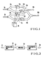
- FIG. 1 is a schematic view illustrating a first embodiment of the optical switch circuit according to the present invention wherein the optical switch circuit having two-input and two-output is also referred to for the brevity of the explanation.
- Light signals transmitted via input light transmission channels lla and llb are optically coupled to fiber-fused star-couplers 12a and 12b serving as light splitters, respectively. Each light signal is split into two light signals by each star-coupler. That is, input light signals are split into four light signals in total.
- the two light signals split by the star-coupler 12a are inputted to optical gate switches 13a and 13b, respectively, and the two light signals split by the star-coupler 12b are inputted to optical gate switches 13c and 13d, respectively.
- the gate switches 13a, 13b, 13c and 13d are constituted by the repeater systems as previously described. Each gate switch is connected to a switch control unit 15, thus being subject to a control such that it is switched to a desired on/off state.
- the switch control unit 15 may be configured so as to allow a bias voltage for each element in the repeater to be changed in accordance with a control signal, and to produce a signal for opening or closing the gate of the FET gate switch, although the configuration of the switch control unit 15 is somewhat different depending upon the fact that which method is employed among the methods for realizing on/off operation of the repeater.
- the switch control unit 15 may be comprised of a multichannel logic circuit.
- the switch control unit 15 can be constituted in combination by the above-mentioned logic circuit and the E/O converter (comprising in combination a drive circuit i and a light emitting element), thus making it possible to transmit a control signal in the form of light by means of an optical fiber. In this instance, problems due to interference between the control signal and an electric signal in the repeater can be perfectly eliminated.
- An optical combiner 14a is connected to the respective outputs of the optical gate switches 13a and 13c.
- an optical combiner 14b is connected to the respective outputs of the optical gate switches 13b and 13d.
- the outputs of the light combiners 14a and 14b are connected to output transmission channels 16a and 16b, respectively.
- the optical switch circuit shown in Fig. 1 is elementarily the same configuration as that of the previously described optical splitter-optical gate type switch circuit, leading to the possibility that the switch is small-sized and multichannel is realized. Further, since the repeater system capable of providing a large extinction ratio is used as each of the optical gate switches 13a, 13b, 13c and 13d, it is possible to realize small crosstalk and to amplify signals without taking into account the nature of incident light. Meanwhile, since the above-mentioned switch circuit is configured such that a light signal is converted once into an electric signal, there is a possibility that limited transmission bandwidth or occurrence of distortion may be caused as compared to the case where switching is effected with the entire signals being in the form of light signals.
- the switch circuit of this embodiment is applicable not only to the switching of high speed digital signal, but also to the switcing of broadband analog signal.
- the ordinary LD was used as a light emitting element in the repeater, but the present invention is not limited to this embodiment.
- the second embodiment is characterized in that a bifacial sensitive area type optical gate switch array is realized by making use of a device configured so that both side surfaces are used as light-receiving and light-emitting areas, respectively.
- Fig. 5 is an explanatory view showing an embodiment of one component of such an optical gate switch array.
- a collector layer 51a of n'-GaAs, a base layer 51b of P-GaAs, an emitter layer 51c of n - -GaAlAs and a layer 51d of n +- GaAs are grown on one surface of a substrate 50 of n -GaAs to form a phototransistor as a light receiving element.
- a cladding layer 52a of n-GaAlAs, an active layer 52b of n -GaAlAs, a cladding layer 52c of P-GaAlAs and a layer 52d of P ⁇ GaAs are grown on the other surface of the substrate 50 of n +- GaAs to form a light emitting diode as a light emitting element.
- electrodes 53 and 54 for biasing are provided on both surface of the substrate 50, respectively.
- Such a gate switch array having a light receiving element formed on one side and a light emitting element formed on the other surface is described in IEEE TRANSACTIONS ON ELECTRON DEVICES vol. ED-28 (1983), 404.
- a single unit obtained by combining the phototransistor with the light emitting diode is used as a unitary light amplifier.
- the above-mentioned device is configured so that light-receiving and light-emitting areas are formed on both surfaces of a single substrate, respectively. Accordingly, an optical matrix switch circuit can be constituted by integrating a large number of these light-receiving and light-emitting areas on both surfaces of a single substrate in a matrix manner, respectively.
- Fig. 6 is a perspective view illustrating an embodiment of a (4 x 4) optical splitter-optical gate type optical switch circuit according to the present invention.
- the optical switch circuit of this embodiment comprises planer type optical splitters 61a, 61b, 61c and 61d each constituted by a guide of Si0 2 system with a SiO 2 film on a Si substrate being as a cladding layer, an optical gate switch array 62 (comprising 16 optical gate switches) formed by integrateing in a matrix manner phototransistors as light receiving elements on one surface of the above-mentioned substrate designated at 60 and light emitting diodes as light emitting elements on the other surface thereof, respectively, and optical combiners 63a, 63b, 63c and 63d for outputs, each of which is constituted so that an optical splitter similar to the above is arranged in an opposite direction wherein the setting is made such that pitches between each waveguide path and the light-receiving and light-emitting elements are equal to each other.
- each optical splitter An input light signal to each optical splitter is split and then is inputted to each optical gate switch.
- An arbitrary switching condition can be selected depending upon on/off state of each optical gate switch.
- a signal corresponding to the selected switching condition is derived as an output light signal via the corresponding output waveguide path.
- the unit optical gate switch is configured as bifacial sensitive area type device in a manner that the phototransistor as a light-receiving element and the LED as a light-emitting diode are formed on both surfaces of the substrate, respectively.
- the optical switch circuit when configured by using a plurality of such unit devices, light-receiving and light-emitting areas will be arranged in a matrix manner on both surfaces of the substrate, respectively, as shown in Fig. 6.
- this allows one surface to serve as light-receiving area and the other surface to serve as light-emitting area.
- optical splitters to which input light signals are transmitted and the output wave guide paths are optically connected to the light-receiving and the light-emitting areas, respectively, thus making it possible to effectively avoid that optical wiring becomes complicated. It is also obvious that multichannel configuration can be easily implemented.
- Fig. 7 is a schematic view illustrating a third embodiment of an optical switch circuit according to the present invention.
- An optical transmission system having for use in 1 micron band is now assumed and a two-input, two output optical switch circuit will be described.
- Light signals transmitted via input optical transmission channels lla and llb are split by optical splitters 12a and 12b each comprised of a fiber-used coupler and then the split light signals are incident to O/E converter means 22a, 22b, 22c and 22d each comprising an InGaAs/InP photodiode and an FET preamplifier, respectively.
- Electric signals outputted from the O/E converter means 22a, 22b, 22c and 22d are amplified by amplifiers 24a, 24b, 24c and 24d, respectively, to allow E/O converter means 25a, 25b, 25c and 25d each comprising a driver circuit and an InGaAsP/InP semiconductor laser diode (LD) to be operative.
- the InGaAsP/InP LD assembled in each E/O converter means is operative to produce an oscillation wavelength variable over a range from 1.2 to 1.55 micron by adjusting the composition ratio of InGaAsP.
- the setting is made such that each wavelength of the E/O converter means 25a and 25c is approximately 1.2 micron and each wavelength of the E/O converter means 25b and 25d is approximately 1.3 micron.
- Output light signals from the E/O converter means 25a, 25b, 25c and 25d are collimated by lenses 71a, 71b, 7lc and 71d, respectively.
- the output light signals thus collimated are optically combined by interference filters 72a and 72b with their optical axes being coincident with each other by making use of the difference between wavelengths.
- the combined two light beams are optically coupled to output optical transmission channels 16a and 16b with high efficiency by means of lenses 73a and 73b, respectively.
- the switching operation required for the optical switch circuit is performed by allowing the control unit 15 to be operative so as to provide, in accordance with a preselected switching condition, a gate signal to each of the FET gate switches provided in interstages of the amplifiers 24a, 24b, 24c and 24d and a bias voltage to the LDs of the E/O converter means 25a, 25b, 25c and 25d.
- the interference filter was used as means for optically combining light by making use of the difference between wavelengths.
- the present invention is not limited to this embodiment.
- the optical splitter is configured by utilizing an optical grating, it is possible to optically combine light having wavelengths which are closer to each other because of its high resolution of the wavelength. This is advantageous in implementation of multichannel of the optical switch circuit.
- a waveguide type wavelength multiplexer of a structure such that a grating is formed on a waveguide path, it is possible to make the device small-sized and realize integrated configuration.
- a waveguide type wavelength multiplexer of InGaAsP/InP system it is possible to monolithically integrate it with each LD of the E/O converter means 25a, 25b, 25c and 25d.
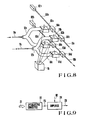
- Fig. 8 is a perspective view illustrating a fourth embodiment according to the present invention wherein an example of a two-input, two-output optical switch is also shown for the brevity of the description.
- Light signals transmitted via input optical trasnmission channels lla and llb are coupled to star-couplers 12d and 12b serving as optical splitters, repectively. Each light signal thus coupled is split into two light signals. That is, input light signals are split into four light signals in total.
- Two light signals transmitted via the star-coupler 12a are inputted to optoelectronic gates 81a and 8lc and two light signals transmitted via the star-coupler 12b are inputted to optoelectronic gates 8lb and 81d.
- Each optoelectronic gate is configured as a module comprising an O/E converter and an amplifier stage as described later.
- These optoelectronic gates 81a, 81b, 81c and 81d are connected to the switch control unit 15 so that a desired on/off switching condition can be realized.
- a dc light signal supplied from a dc light source 82a is inputted to a light modulator 84a to which an output electric signal outputted from the optoelectronic gate 81a is applied through an optical waveguide path 83a.
- the output light of the light modulator 84a passes through an optical waveguide path 83b and an optical modulator 84b to which an electric signal outputted from the optoelectronic gate 81b is applied, and then is transmitted to the output optical transmission path 16a.
- a dc light signal supplied from a dc light source 8.2b is inputted to an optical modulator 84c to which an electric signal outputted from the optoelectronic gate 81c is applied through an optical wavepath 83c.
- the output light of a light modulator 84c passes through an optical waveguide path 83d and a light modulator 84d to which an electric signal outputted from the optoelectronic gate 81d is applied, and then is transmitted to the output transmission path 16b.
- Fig. 9 is a block diagram illustrating the circuit configuration of the optoelectronic gates 81a, 81b, 81c and 81d shown in Fig. 8.
- An incident light signal 21 is converted into an electric signal 23 by an 0/E converter means 22.
- the electric signal 23 is outputted as a modulation signal 26 via a suitable amplifier circuit 24.
- the modulation signal 26 changes to either a dc signal or a signal obtained by amplifying the electric signal 23 in accordance with a control signal 90 supplied from the switch control unit 15.
- Fig. 10 is a timing chart for explaining the operation of the embodiment shown in Fig. 8.
- reference numerals 101 and 104 denote an input light signal to the input optical transmission path lla (Fig. 8) and an input light signal to the input optical transmission path 11b (Fib. 8), respectively.
- the switching is effected in a manner that the light signal 101 is outputted to the output optical transmission path 16a during a period from time T 1 to T Z (time period ⁇ 1 ) and the light signal 104 is outputted thereto during a period from time T 2 to T 3 (time period ⁇ 2 ).
- the optoelectronic gate 81a is operative during the time period ⁇ 1 so as to output a modulation signal obtained by optoelectronic-converting and amplifying the light signal 101, and is operative during the time period T2 so as to output a modulation signal of a constant voltage V 1 .
- the modulation signal 102 of such a nature, a dc light input from the dc light source 82a to the optical modulator 84a via the optical waveguide path 83a is modulated.
- a light signal outputted from the light modulator 84a to the optical waveguide path 83b has a waveform similar to that of the modulation signal 102, i.e., it has the same waveform as that of the light signal 101 during the time period T 1 and becomes a dc light of a constant level P 1 during the time period ⁇ 2 .
- the optoelectronic gate 81b is operative during the time period ⁇ 1 so as to output a modulation signal of a constant voltage V l , and is operative during the time period ⁇ 2 so as to output a modulation signal obtained by optoelectronic-converting and amplifying the light signal 104.
- the modulation signal 105 a light signal 103 inputted to the light modulator 84b via the .optical waveguide path 83b is modulated.
- a light signal outputted from the light modulator 84b to the output optical transmission path 16a has a waveform similar to that of the light signal 101 during the time period ⁇ 1 and has a waveform similar to that of the light signal 104.
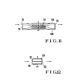
- Fig. 11 is a schematic view illustrating a first example of the light modulators 84a, 84b, 84c and 84d in the embodiment shown in Fig. 8.
- Optical waveguide paths 112a and 112b are formed close to each other on a crystalline substrate 111 having electro-optical effect so that they are operable as a directional coupler.
- a light signal incident on one end surface 113 of the optical waveguide path 112a is modulated by a modulation signal applied between electrodes 114, and then is outputted from the other end surface 115.
- a small optical loss is expected.
- optical modulator array can be formed by integrating a plurality of such light modulators on one crystalline substrate.
- the light modulator having such an electro-optical effect is described in detail in IEEE TRANSACTIONS ON Microwave Theory and Techniques, Vol. 1, MIT-30, No. 8, August, 1982.
- FIG. 12 is a schematic view illustrating a second example of the light modulators 84a, 84b, 84c and 84d employed in the embodiment shown in Fig. 8.
- a light signal inputted to one end surface of an active layer of a semiconductor laser 121 is modulated by a modulation signal applied to an electrode 124.
- the light signal thus modulated is outputted from the other end surface 123 of the active layer.
- Such a light modulator using a semiconductor laser can provide optical amplification.
- the light modulator using such a semiconductor laser is described in the article of IEEE Journal of Quantum Electron vol. QE-19, p. 157, 1983.
- the present invention can provide an optical switch circuit which is samll-sized and is suitable for integration, which is of a small crosstalk thereby being able to effect a high speed switching without distortion of a broadband signal, and which has a wide application such that light transmitted through a multimode optical fiber can be switched, thus significantly contributing to the realization of various kinds of optical systems in future.
Landscapes
- Optical Communication System (AREA)
Applications Claiming Priority (8)
| Application Number | Priority Date | Filing Date | Title |
|---|---|---|---|
| JP59099120A JPS60242723A (ja) | 1984-05-17 | 1984-05-17 | 光スイツチ回路 |
| JP99120/84 | 1984-05-17 | ||
| JP128715/84 | 1984-06-22 | ||
| JP59128715A JPS617739A (ja) | 1984-06-22 | 1984-06-22 | 光スイツチ回路 |
| JP72153/85 | 1985-04-05 | ||
| JP7215385A JPS61231530A (ja) | 1985-04-05 | 1985-04-05 | 光スイツチ回路 |
| JP7630485A JPS61235823A (ja) | 1985-04-10 | 1985-04-10 | 光スイツチ回路 |
| JP76304/85 | 1985-04-10 |
Publications (3)
| Publication Number | Publication Date |
|---|---|
| EP0161683A2 true EP0161683A2 (fr) | 1985-11-21 |
| EP0161683A3 EP0161683A3 (en) | 1988-08-03 |
| EP0161683B1 EP0161683B1 (fr) | 1993-08-11 |
Family
ID=27465439
Family Applications (1)
| Application Number | Title | Priority Date | Filing Date |
|---|---|---|---|
| EP85106005A Expired - Lifetime EP0161683B1 (fr) | 1984-05-17 | 1985-05-15 | Circuit commutateur optique |
Country Status (4)
| Country | Link |
|---|---|
| US (1) | US4798435A (fr) |
| EP (1) | EP0161683B1 (fr) |
| CA (1) | CA1257924A (fr) |
| DE (1) | DE3587515T2 (fr) |
Cited By (6)
| Publication number | Priority date | Publication date | Assignee | Title |
|---|---|---|---|---|
| EP0277779A1 (fr) * | 1987-01-29 | 1988-08-10 | BRITISH TELECOMMUNICATIONS public limited company | Coupleur spatial optique |
| US4901305A (en) * | 1987-12-28 | 1990-02-13 | Tangonan Gregory L | Distributed crossbar switch |
| US4952010A (en) * | 1987-02-20 | 1990-08-28 | British Telecommunications Public Limited Company | Optical space switch |
| US5072439A (en) * | 1990-03-16 | 1991-12-10 | Hughes Aircraft Company | High speed opto-electronic crossbar switch |
| GB2300321A (en) * | 1995-04-26 | 1996-10-30 | Northern Telecom Ltd | Switched optical cross-connect |
| EP3086150A1 (fr) * | 2014-11-05 | 2016-10-26 | The Boeing Company | Conception et mise en oeuvre de système de données bus-in-a-box (bib) |
Families Citing this family (16)
| Publication number | Priority date | Publication date | Assignee | Title |
|---|---|---|---|---|
| GB8707852D0 (en) * | 1987-04-02 | 1987-05-07 | British Telecomm | Optical switch |
| US4952031A (en) * | 1987-06-19 | 1990-08-28 | Victor Company Of Japan, Ltd. | Liquid crystal display device |
| US4934775A (en) * | 1989-01-18 | 1990-06-19 | Gte Laboratories Incorporated | Optical space switches using cascaded coupled-waveguide optical gate arrays |
| US5004447A (en) * | 1989-09-06 | 1991-04-02 | The United States Of America As Represented By The Secretary Of The Air Force | Low loss semiconductor directional coupler switches including gain method of switching light using same |
| US5274487A (en) * | 1989-12-29 | 1993-12-28 | Fujitsu Limited | Photonic switching system |
| EP0782809B1 (fr) * | 1994-09-14 | 2001-02-28 | Siemens Aktiengesellschaft | Matrice de commutation optique 1xn et nxn arborescente |
| DE4437325A1 (de) * | 1994-10-19 | 1996-04-25 | Bosch Gmbh Robert | Optischer Schalter und optisches Koppelfeld damit |
| US5710846A (en) * | 1996-03-26 | 1998-01-20 | Rf Systems, Inc. | Self-calibrating optical fiber switch |
| US6768572B2 (en) | 1997-10-29 | 2004-07-27 | Teloptics Corporation | Solid state free space switch array on a substrate |
| US6310712B1 (en) | 1997-10-29 | 2001-10-30 | Teloptics Corporation | Discrete element light modulating microstructure devices |
| US6816296B2 (en) | 1997-10-29 | 2004-11-09 | Teloptics Corporation | Optical switching network and network node and method of optical switching |
| US6486996B1 (en) | 1998-10-27 | 2002-11-26 | Teloptics Corporations | Discrete element light modulating microstructure devices |
| EP1362251B1 (fr) | 2000-12-13 | 2007-08-22 | BAE SYSTEMS Information and Electronic Systems Integration, Inc. | Reseau de signaux photoniques a circuits integres |
| US20030010992A1 (en) * | 2001-07-16 | 2003-01-16 | Motorola, Inc. | Semiconductor structure and method for implementing cross-point switch functionality |
| US6958598B2 (en) * | 2003-09-30 | 2005-10-25 | Teradyne, Inc. | Efficient switching architecture with reduced stub lengths |
| US7964883B2 (en) * | 2004-02-26 | 2011-06-21 | Lighting Science Group Corporation | Light emitting diode package assembly that emulates the light pattern produced by an incandescent filament bulb |
Citations (5)
| Publication number | Priority date | Publication date | Assignee | Title |
|---|---|---|---|---|
| US4381881A (en) * | 1980-05-27 | 1983-05-03 | The United States Of America As Represented By The Administrator Of The National Aeronautics And Space Administration | Fiber optic crossbar switch for automatically patching optical signals |
| JPS5897994A (ja) * | 1981-12-08 | 1983-06-10 | Nippon Telegr & Teleph Corp <Ntt> | 交換用スイツチ |
| DE3218737A1 (de) * | 1982-05-18 | 1983-11-24 | Institut für Rundfunktechnik GmbH, 8000 München | Lichtwellenleiter-vermittlungssystem |
| FR2528586A1 (fr) * | 1982-06-11 | 1983-12-16 | Cit Alcatel | Dispositif de commutation optique |
| FR2547071A1 (fr) * | 1983-05-31 | 1984-12-07 | Cit Alcatel | Dispositif opto-electronique de commutation spatiale |
Family Cites Families (4)
| Publication number | Priority date | Publication date | Assignee | Title |
|---|---|---|---|---|
| US3871743A (en) * | 1973-06-04 | 1975-03-18 | Gte Laboratories Inc | Optical crosspoint switching matrix for an optical communications system |
| US4011543A (en) * | 1976-02-20 | 1977-03-08 | Sperry Rand Corporation | Low crosstalk optical switch |
| US4153329A (en) * | 1977-07-25 | 1979-05-08 | Bell Telephone Laboratories, Incorporated | Optical crosspoint switch having mode-conversion facilities |
| NL8204722A (nl) * | 1982-12-07 | 1984-07-02 | Philips Nv | Distributiesysteem voor lokaal fibernet. |
-
1985
- 1985-05-15 DE DE85106005T patent/DE3587515T2/de not_active Expired - Lifetime
- 1985-05-15 EP EP85106005A patent/EP0161683B1/fr not_active Expired - Lifetime
- 1985-05-16 US US06/734,725 patent/US4798435A/en not_active Expired - Lifetime
- 1985-05-16 CA CA000481666A patent/CA1257924A/fr not_active Expired
Patent Citations (5)
| Publication number | Priority date | Publication date | Assignee | Title |
|---|---|---|---|---|
| US4381881A (en) * | 1980-05-27 | 1983-05-03 | The United States Of America As Represented By The Administrator Of The National Aeronautics And Space Administration | Fiber optic crossbar switch for automatically patching optical signals |
| JPS5897994A (ja) * | 1981-12-08 | 1983-06-10 | Nippon Telegr & Teleph Corp <Ntt> | 交換用スイツチ |
| DE3218737A1 (de) * | 1982-05-18 | 1983-11-24 | Institut für Rundfunktechnik GmbH, 8000 München | Lichtwellenleiter-vermittlungssystem |
| FR2528586A1 (fr) * | 1982-06-11 | 1983-12-16 | Cit Alcatel | Dispositif de commutation optique |
| FR2547071A1 (fr) * | 1983-05-31 | 1984-12-07 | Cit Alcatel | Dispositif opto-electronique de commutation spatiale |
Non-Patent Citations (3)
| Title |
|---|
| APPLIED PHYSICS LETTERS, vol. 35, no. 10, 15th November 1979, pages 795-796, American Institute of Physics, New York, US; M. YUST et al.: "A monolithically integrated optical repeater" * |
| IEEE TRANSACTIONS ON ELECTRON DEVICES, vol. ED-28, no. 4, April 1981, pages 404-407, IEEE, New York, US; H. BENEKING et al.: "Monolithic GaAlAs/GaAs infrared-to-visible wavelength converter with optical power amplification" * |
| PATENT ABSTRACTS OF JAPAN, vol. 7, no. 200 (E-196)[1345], 3rd September 1983; & JP-A-58 97 994 (NIPPON DENSHIN DENWA KOSHA) 10-06-1983 * |
Cited By (11)
| Publication number | Priority date | Publication date | Assignee | Title |
|---|---|---|---|---|
| EP0277779A1 (fr) * | 1987-01-29 | 1988-08-10 | BRITISH TELECOMMUNICATIONS public limited company | Coupleur spatial optique |
| WO1988005986A1 (fr) * | 1987-01-29 | 1988-08-11 | British Telecommunications Public Limited Company | Commutateur spatial optique bidirectionnel |
| US4923269A (en) * | 1987-01-29 | 1990-05-08 | British Telecommunications Public Limited Company | Bidirectional optical space switch |
| AU597149B2 (en) * | 1987-01-29 | 1990-05-24 | British Telecommunications Public Limited Company | Bidirectional optical space switch |
| US4952010A (en) * | 1987-02-20 | 1990-08-28 | British Telecommunications Public Limited Company | Optical space switch |
| US4901305A (en) * | 1987-12-28 | 1990-02-13 | Tangonan Gregory L | Distributed crossbar switch |
| US5072439A (en) * | 1990-03-16 | 1991-12-10 | Hughes Aircraft Company | High speed opto-electronic crossbar switch |
| GB2300321A (en) * | 1995-04-26 | 1996-10-30 | Northern Telecom Ltd | Switched optical cross-connect |
| EP3086150A1 (fr) * | 2014-11-05 | 2016-10-26 | The Boeing Company | Conception et mise en oeuvre de système de données bus-in-a-box (bib) |
| US9791644B2 (en) | 2014-11-05 | 2017-10-17 | The Boeing Company | Data bus-in-a-box (BiB) system design and implementation |
| RU2690032C2 (ru) * | 2014-11-05 | 2019-05-30 | Зе Боинг Компани | Конструкция и реализации системы для коробки с шиной данных ("data bus-in-a-box") |
Also Published As
| Publication number | Publication date |
|---|---|
| CA1257924A (fr) | 1989-07-25 |
| US4798435A (en) | 1989-01-17 |
| EP0161683A3 (en) | 1988-08-03 |
| EP0161683B1 (fr) | 1993-08-11 |
| DE3587515T2 (de) | 1994-03-17 |
| DE3587515D1 (de) | 1993-09-16 |
Similar Documents
| Publication | Publication Date | Title |
|---|---|---|
| US4798435A (en) | Optical switch circuit | |
| US6490044B1 (en) | Optimized interferometrically modulated array source | |
| CA1298388C (fr) | Dispositif optique symetrique | |
| US6680791B2 (en) | Semiconductor device for rapid optical switch by modulated absorption | |
| CA1293795C (fr) | Dispositif optique | |
| JP2004029811A (ja) | 導波型光クロスポイントスイッチ | |
| US7010230B2 (en) | Integrated high-speed multiple-rate optical-time-division-multiplexing module | |
| WO2005104404A2 (fr) | Thyristor et circuit integre optoelectronique multifonctionnel et emetteur-recepteur optique comprenant ceux-ci | |
| US4887877A (en) | Optical devices and optical integrated circuits | |
| US20030206691A1 (en) | High speed data link and transmitter in the mid-infrared wavelength range | |
| US4810050A (en) | Optical inverter and logic devices using same with buffer limited electrical interface | |
| CA2267018C (fr) | Convertisseur de longueurs d'ondes optique avec guide d'ondes actif | |
| EP1314333B1 (fr) | Routeur optique integre et matrice de conversion de longueur d'onde | |
| JP3147570B2 (ja) | 光通信装置 | |
| JP2630052B2 (ja) | マトリクス光スイッチ | |
| US5247592A (en) | Semiconductor optical device and array of the same | |
| Lu et al. | High-speed, cascaded optical logic operations using programmable optical logic gate arrays | |
| Lentine et al. | Optoelectronic VLSI switching chip with greater than 4000 optical I/O based on flip chip bonding of GaAs-AlGaAs MQW modulators and detectors to silicon CMOS | |
| JPH07106548A (ja) | 半導体光源装置とその駆動方法 | |
| Maeda et al. | Integrated optoelectronics for optical transmission systems | |
| US7466914B2 (en) | Optoelectronic switch having cascaded optical nodes | |
| JPH0731330B2 (ja) | マトリクススイツチ及びその駆動方法 | |
| JP2923969B2 (ja) | 光スイッチ | |
| JPS60242723A (ja) | 光スイツチ回路 | |
| JP2622576B2 (ja) | 光信号変換装置 |
Legal Events
| Date | Code | Title | Description |
|---|---|---|---|
| PUAI | Public reference made under article 153(3) epc to a published international application that has entered the european phase |
Free format text: ORIGINAL CODE: 0009012 |
|
| 17P | Request for examination filed |
Effective date: 19850515 |
|
| AK | Designated contracting states |
Designated state(s): DE FR GB |
|
| PUAL | Search report despatched |
Free format text: ORIGINAL CODE: 0009013 |
|
| AK | Designated contracting states |
Kind code of ref document: A3 Designated state(s): DE FR GB |
|
| 17Q | First examination report despatched |
Effective date: 19900911 |
|
| GRAA | (expected) grant |
Free format text: ORIGINAL CODE: 0009210 |
|
| AK | Designated contracting states |
Kind code of ref document: B1 Designated state(s): DE FR GB |
|
| REF | Corresponds to: |
Ref document number: 3587515 Country of ref document: DE Date of ref document: 19930916 |
|
| ET | Fr: translation filed | ||
| PLBE | No opposition filed within time limit |
Free format text: ORIGINAL CODE: 0009261 |
|
| STAA | Information on the status of an ep patent application or granted ep patent |
Free format text: STATUS: NO OPPOSITION FILED WITHIN TIME LIMIT |
|
| 26N | No opposition filed | ||
| REG | Reference to a national code |
Ref country code: GB Ref legal event code: IF02 |
|
| PGFP | Annual fee paid to national office [announced via postgrant information from national office to epo] |
Ref country code: FR Payment date: 20040510 Year of fee payment: 20 |
|
| PGFP | Annual fee paid to national office [announced via postgrant information from national office to epo] |
Ref country code: GB Payment date: 20040512 Year of fee payment: 20 |
|
| PGFP | Annual fee paid to national office [announced via postgrant information from national office to epo] |
Ref country code: DE Payment date: 20040527 Year of fee payment: 20 |
|
| PG25 | Lapsed in a contracting state [announced via postgrant information from national office to epo] |
Ref country code: GB Free format text: LAPSE BECAUSE OF EXPIRATION OF PROTECTION Effective date: 20050514 |
|
| REG | Reference to a national code |
Ref country code: GB Ref legal event code: PE20 |