EP0160531B1 - Demodulator circuits for amplitude-modulated signals - Google Patents
Demodulator circuits for amplitude-modulated signals Download PDFInfo
- Publication number
- EP0160531B1 EP0160531B1 EP85302933A EP85302933A EP0160531B1 EP 0160531 B1 EP0160531 B1 EP 0160531B1 EP 85302933 A EP85302933 A EP 85302933A EP 85302933 A EP85302933 A EP 85302933A EP 0160531 B1 EP0160531 B1 EP 0160531B1
- Authority
- EP
- European Patent Office
- Prior art keywords
- signal
- demodulator
- demodulating
- level
- modulated
- Prior art date
- Legal status (The legal status is an assumption and is not a legal conclusion. Google has not performed a legal analysis and makes no representation as to the accuracy of the status listed.)
- Expired
Links
Images
Classifications
-
- H—ELECTRICITY
- H04—ELECTRIC COMMUNICATION TECHNIQUE
- H04N—PICTORIAL COMMUNICATION, e.g. TELEVISION
- H04N9/00—Details of colour television systems
- H04N9/64—Circuits for processing colour signals
- H04N9/66—Circuits for processing colour signals for synchronous demodulators
Definitions
- This invention relates to demodulator circuits for amplitude-modulated signals, for example, signals transmitted between the output of a colour video camera and a camera control unit (hereinafter referred to as a CCU).
- a CCU camera control unit
- Video signals are transmitted from the output of a video camera to a CCU over a cable, and returning video signals from the CCU are transmitted over the same cable.
- the luminance signal in the video signal from the video camera is amplitude-modulated onto a fixed frequency carrier wave, and the two colour difference signals are quadrature two-phase amplitude-modulated before being transmitted.
- amplitude- demodulation is effected to derive the original luminance signal and the two colour difference signals.
- a previously proposed demodulator circuit for the amplitude-modulated signals operates by passing the input signal through a band-pass filter and a limiter to extract the carrier signal, and supplying it to a phase-locked loop (PLL) circuit, in which a carrier signal for use in the demodulation is generated.
- PLL phase-locked loop
- Such a demodulator circuit does however have defects.
- the phase of the output ofthe limiter depends on the input level, so the phase of the carrier signal for synchronous demodulation is of low accuracy, and there is a substantial risk of unstable operation prior to settlement into the locked state of the PLL circuit due to the limited loop gain of the PLL circuit.
- a demodulator circuit for an amplitude-modulated signal comprising:
- the invention will be described by way of example with reference to the transmission of a colour video signal from a video camera to a CCU over a camera cable.
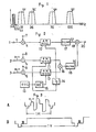
- Figure 1 indicates the frequency spectra of the signals transmitted between the CCU and the video camera. From the CCU to the video camera, a return video signal (composite video signal), a video signal for a teleprompter, an intercom signal and a programme audio signal are transmitted.
- SR represents the frequency-modulated return video signal of 70 MHz carrier frequency
- ST represents the frequency-modulated video signal of 100 MHz carrier frequency for the teleprompter.
- the frequency-modulated intercom signal has a carrier frequency of 3 MHz
- the frequency-modulated programme audio signal has a carrier frequency of 4 MHz.
- the programme audio signal is the audio signal to be broadcast.
- an amplitude-modulated luminance signal SY of 18 MHz carrier frequency the colour difference signal SC consisting of the R-Y signal and the B-Y signal which have been quadrature two-phase amplitude modulated and have a carrier frequency of 36 MHz, frequency-modulated microphone signals for two channels having 5 MHz and 5.5 MHz carrier frequencies, respectively, a frequency-modulated intercom signal of 6 MHz carrier frequency, and a discrimination signal having a carrier frequency of 6.5 MHz.
- FIG. 2 is a block diagram of a circuit provided in the video camera unit for generating the above- mentioned signals SY and SC.
- the circuit comprises an input terminal 1 for receiving luminance signals from the output of a video camera (not shown), an input terminal 2 for receiving an R-Y signal from the output of the video camera, and an input terminal 3 for receiving a B-Y signal from the output of the video camera.
- the input luminance, R-Y and B-Y signals are supplied to respective adders 4, and 6.
- the adder 4 is also supplied with a synchronizing signal of the horizontal period from a terminal 7.
- the adder 5 is also supplied with a discrimination signal such as a synchronizing signal of the horizontal period from a terminal 8.
- the adder 6 is also supplied with another discrimination signal such as a burst signal from a terminal 9.
- the output from the adder 4 is supplied to an amplitude-modulator 10, to which the carrier signal of 18 MHz from a 1/2 frequency divider circuit 14, which receives a 36 MHz carrier signal generated by an oscillator 13 is also fed.
- the output of the adder 5 is supplied to another amplitude-modulator 11, which also receives the carrier signal directly from the oscillator 13.
- the output of the adder 6 is supplied to another amplitude-modulator 12 which additionally receives the 90°-shifted signal from a 90° phase shifter 15 which receives the carrier signal from the oscillator 13.
- the outputs of the amplitude- modulators 11 and 12 are fed to another adder 16.
- the output of the amplitude-modulator 10 is supplied to another adder 19 through a filter 17, and the output of the adder 16 is supplied to the adder 19 through a filter 18.
- the filters 17 and 18 are provided for the elimination of unnecessary signals.
- the filter 17 supplies the amplitude-modulated luminance signals SY having a centre frequency of 18 MHz.
- the filter 18 supplies the quadrature two-phase amplitude modulated colour difference signals with a centre frequency of 36 MHz forming the signal SC.
- the output of the adder 19 is transmitted to the CCU over a camera cable through an output terminal 20.
- the synchronous signal to be mixed with the luminance signal and the R-Y signal may be a signal of the horizontal period or an integral multiple thereof, and is not limited to a composite synchronization signal.
- Figure 3A shows the waveform of a signal consisting of the R-Y signal plus a synchronous signal superimposed onto it. Additionally, a burst signal to be superimposed on to the B-Y signal is, for example, a sine wave of 4.5 MHz, which may be obtained by frequency- division of the output of the oscillator 13. As shown in Figure 3B, the burst signal is inserted during one horizontal period following every vertical period.
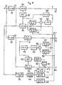
- Figure 4 shows a block diagram of a demodulator circuit for demodulating such signals from the video camera and transmitted to the CCU over the camera cable.
- the demodulator circuit includes an input terminal 31 for receiving the signals which are fed to filters 32 and 33.
- the filter 32 derives the amplitude-modulated luminance signal SY
- the filter 33 derives the quadrature two-phase amplitude-modulated colour difference signal SC.
- the amplitude-modulated luminance signal SY is fed to synchronous demodulators 34 and 35, and to an envelope detector 36.
- the luminance signal Y is developed at the output of the synchronous demodulator 34 and is supplied to an output terminal 37.
- the output signal of a voltage controlled oscillator (VCO) 38 is fed to the synchronous demodulator 35 as a carrier signal.
- a carrier signal is also fed from the VCO 38 to the synchronous demodulator 34 through a 90° phase shifter 39.
- the demodulator circuit also includes a synchronous signal sample-hold circuit 40 and a black level sample-hold circuit 41.
- the sample-hold circuits 40 and 41 receive the output signal of the synchronous demodulator 35, and feed their outputs to a subtraction circuit 42.
- the output of the subtraction circuit 42 is fed as a control signal to the VCO 38 through a low-pass filter 43.
- the amplitude-modulated colour difference signal SC is supplied from the filter 33 and fed to synchronous demodulators 51 and 52.
- the output of the synchronous demodulator 51 is the B-Y signal and is supplied to an output terminal 53.
- the output of the synchronous demodulator 52 is the R-Y signal and is supplied to an output terminal 54.
- the output of the synchronous demodulator 51 is also fed to a synchronizing signal sample-hold circuit 57 and to a black level sample-hold circuit 58, the outputs of which are fed to another subtractor 59 for error detection.
- the output of the subtractor 59 is supplied as the control signal for a VCO 55 through another low-pass filter 60.
- the output of the VCO 55 forms carrier signals supplied to the synchronous demodulator 51, and to the synchronous demodulator 52 through a 90° phase shifter 56.
- the output of the synchronous demodulator 52 is fed to a level detector 62 through another burst signal sample-hold circuit 61.
- the output of the level detector 62 is supplied as a phase control voltage to the 90° phase shifter 56.
- Sampling pulses are fed from a pulse generator 45 to the sample-hold circuits 40 and 57, from another pulse generator 46 to the sample-hold circuits 41 and 58, and from a pulse generator 47 to the sample-hold circuit 61.
- sampling pulses for sample-holding the synchronizing signal are formed in the pulse generator 45, sampling pulses for sample-holding of the black level are formed in the pulse generator 46, and sampling pulses for sample-holding the burst signal are formed in the pulse generator 47.
- the luminance signal demodulating system comprises the subtractor 42, the low-pass filter 43, the VCO 38 and the two sample-hold circuits 40 and 41, which form a PLL circuit.
- the VCO 38 is controlled in phase so that the level of the output of the subtraction circuit 42 is zero. In this condition, the phase of the carrier signal generated by the VCO 38 differs by 90° from the normal demodulating axis of the amplitude-modulated signal.
- the output signal of the VCO 38 is supplied to the synchronous demodulator 34 through a 90° phase shifter 39, so the synchronous demodulator 34 derives the luminance signal Y.
- Detection of the level of the synchronizing signal is made with reference to the black level to prevent influence by the level of the video signal (APL). If there is provided a clamp circuit for bringing the black level to a fixed level, however, only the level of the synchronizing signal need be detected.
- the B-Y signal demodulation system comprises the subtractor 59, the low-pass filter 60, the VCO 55 and the two sample-hold circuits 57 and 58, which form a PLL circuit.
- the VCO 55 is controlled so that the level of the output of the subtractor 59 is zero, that is, the level of the synchronizing signal is zero.
- the phase of the carrier signal output from the VCO 55 coincides with the normal demodulating axis of the amplitude-modulated B-Y signal. That is to say, the synchronizing signal is incorporated only in the R-Y signal, and so no synchronizing signal component is developed in the output of the synchronous demodulator 51. This implies that the phase of the carrier signal from the VCO 55 coincides with the demodulating axis of the B-Y signal.
- the output signal of the VCO 55 is fed through the 90° phase shifter 56 to a synchronous demodulator 52, where demodulation is carried out to form the original R-Y signal.
- the closed loop comprising the synchronous demodulator 52, the burst signal sample-hold circuit 61, the level detector 62 and the 90° phase shifter 56 operates so as to bring the level of the burst signal to zero, contributing to prevention of leakage of the B-Y signal into the R-Y signal.
- each signal is fed to a matrix circuit through a synchronizing signal eliminating circuit and a burst signal eliminating circuit (not shown), to be converted into primary colour signals for red, green and yellow.
- the invention is not only applicable to transmission of signals between a video camera and a CCU, but also, for example, to transmission of colour video signals for cable television (CATV).
- CATV cable television
- Embodiments of demodulator circuit according to the present invention can perform stable demodulation without using a limiter, and with the phase of the carrier signal for demodulation free from dependence on the level of the input signals.
Landscapes
- Engineering & Computer Science (AREA)
- Multimedia (AREA)
- Signal Processing (AREA)
- Processing Of Color Television Signals (AREA)
- Color Television Image Signal Generators (AREA)
Applications Claiming Priority (2)
| Application Number | Priority Date | Filing Date | Title |
|---|---|---|---|
| JP59085733A JPS60229596A (ja) | 1984-04-27 | 1984-04-27 | 直交2相変調信号の復調回路 |
| JP85733/84 | 1984-04-27 |
Publications (3)
| Publication Number | Publication Date |
|---|---|
| EP0160531A2 EP0160531A2 (en) | 1985-11-06 |
| EP0160531A3 EP0160531A3 (en) | 1987-03-25 |
| EP0160531B1 true EP0160531B1 (en) | 1991-01-09 |
Family
ID=13867038
Family Applications (1)
| Application Number | Title | Priority Date | Filing Date |
|---|---|---|---|
| EP85302933A Expired EP0160531B1 (en) | 1984-04-27 | 1985-04-25 | Demodulator circuits for amplitude-modulated signals |
Country Status (5)
| Country | Link |
|---|---|
| US (1) | US4633187A (enExample) |
| EP (1) | EP0160531B1 (enExample) |
| JP (1) | JPS60229596A (enExample) |
| CA (1) | CA1239198A (enExample) |
| DE (1) | DE3581225D1 (enExample) |
Families Citing this family (5)
| Publication number | Priority date | Publication date | Assignee | Title |
|---|---|---|---|---|
| JP2964899B2 (ja) * | 1995-02-28 | 1999-10-18 | 日本電気株式会社 | 符号化と復号化周波数同期方法 |
| US5801895A (en) * | 1996-05-28 | 1998-09-01 | Hewlett Packard Company | Disk drive servo demodulation system which suppresses noise on the position error signal |
| EP0849955A3 (en) * | 1996-12-17 | 2000-05-03 | Lg Electronics Inc. | Device and method for generating a composite color signal with digital QAM |
| US5926220A (en) * | 1997-06-18 | 1999-07-20 | C-Cube Microsystems, Inc. | Composite digital video decoder and digital compressor |
| US7679685B2 (en) * | 2006-02-24 | 2010-03-16 | Panasonic Automotive Systems of America division of Panasonic Corporation of North America | System and method for processing video signals |
Family Cites Families (3)
| Publication number | Priority date | Publication date | Assignee | Title |
|---|---|---|---|---|
| US3987481A (en) * | 1974-05-09 | 1976-10-19 | Motorola, Inc. | Color television signal demodulation system |
| FR2368184A1 (fr) * | 1976-10-18 | 1978-05-12 | Ibm France | Systeme de synchronisation de porteuse pour demodulateur de phase coherent |
| DE3272758D1 (en) * | 1981-11-09 | 1986-09-25 | Matsushita Electric Industrial Co Ltd | A synchronous video detector circuit using phase-locked loop |
-
1984
- 1984-04-27 JP JP59085733A patent/JPS60229596A/ja active Granted
-
1985
- 1985-04-25 EP EP85302933A patent/EP0160531B1/en not_active Expired
- 1985-04-25 CA CA000480045A patent/CA1239198A/en not_active Expired
- 1985-04-25 DE DE8585302933T patent/DE3581225D1/de not_active Expired - Lifetime
- 1985-04-26 US US06/727,561 patent/US4633187A/en not_active Expired - Lifetime
Also Published As
| Publication number | Publication date |
|---|---|
| US4633187A (en) | 1986-12-30 |
| EP0160531A2 (en) | 1985-11-06 |
| CA1239198A (en) | 1988-07-12 |
| JPH0574994B2 (enExample) | 1993-10-19 |
| JPS60229596A (ja) | 1985-11-14 |
| DE3581225D1 (de) | 1991-02-14 |
| EP0160531A3 (en) | 1987-03-25 |
Similar Documents
| Publication | Publication Date | Title |
|---|---|---|
| US4514763A (en) | Sound signal and impulse noise detector for television receivers | |
| EP0178868A2 (en) | Chrominance signal processing apparatus | |
| US4975775A (en) | Tuner for receiving television signal in frequency division multiplex system and television signal in time division multiplex system | |
| US6034735A (en) | Clock generator for digital video signal processing apparatus | |
| EP0160531B1 (en) | Demodulator circuits for amplitude-modulated signals | |
| US4686569A (en) | Circuitry for reducing demodulation phase error as for an automatic deghosting system | |
| EP0735779B1 (en) | Color signal demodulator suitable for PAL and SECAM TV receiver | |
| US4800427A (en) | Method of compatibly increasing resolution in a color television system | |
| US3961135A (en) | Synchronized demodulation system | |
| EP0504901B1 (en) | Chrominance signal processing circuit | |
| KR100239600B1 (ko) | 색 신호 복조 회로 | |
| EP0289326B1 (en) | Magnetic recording and reproducing apparatus | |
| JPH0654959B2 (ja) | Am変調ビデオ信号の復調回路 | |
| JP2823291B2 (ja) | Secam方式ライン識別回路 | |
| KR920002840B1 (ko) | 텔레비젼 음성 검출장치 | |
| EP0421434B1 (en) | Circuit for removing jitter of chrominance signal and television set using the same | |
| US5132782A (en) | Interleave detector of composite video signal | |
| EP0939556B1 (en) | Method and apparatus for digital multi-standard colour signal demodulation | |
| KR910008400B1 (ko) | Ac-tv의 보조신호 복조회로 | |
| KR100209963B1 (ko) | Ntsc방식 텔레비전의 virs를 이용한 atc 구현 장치 | |
| JP3253482B2 (ja) | 色信号復調回路 | |
| JPS59156096A (ja) | Pal,secam方式判別回路 | |
| JPS58141092A (ja) | カラ−テレビ受像機における方式自動切換回路 | |
| KR20000043172A (ko) | 두 개의 기준 주파수를 이용한 단일 secam 색신호 복조기 | |
| JPH0879639A (ja) | テレビジョン放送信号受信装置 |
Legal Events
| Date | Code | Title | Description |
|---|---|---|---|
| PUAI | Public reference made under article 153(3) epc to a published international application that has entered the european phase |
Free format text: ORIGINAL CODE: 0009012 |
|
| AK | Designated contracting states |
Designated state(s): DE FR GB NL |
|
| PUAL | Search report despatched |
Free format text: ORIGINAL CODE: 0009013 |
|
| AK | Designated contracting states |
Kind code of ref document: A3 Designated state(s): DE FR GB NL |
|
| 17P | Request for examination filed |
Effective date: 19870821 |
|
| 17Q | First examination report despatched |
Effective date: 19890720 |
|
| GRAA | (expected) grant |
Free format text: ORIGINAL CODE: 0009210 |
|
| AK | Designated contracting states |
Kind code of ref document: B1 Designated state(s): DE FR GB NL |
|
| ET | Fr: translation filed | ||
| REF | Corresponds to: |
Ref document number: 3581225 Country of ref document: DE Date of ref document: 19910214 |
|
| PLBE | No opposition filed within time limit |
Free format text: ORIGINAL CODE: 0009261 |
|
| STAA | Information on the status of an ep patent application or granted ep patent |
Free format text: STATUS: NO OPPOSITION FILED WITHIN TIME LIMIT |
|
| 26N | No opposition filed | ||
| REG | Reference to a national code |
Ref country code: GB Ref legal event code: IF02 |
|
| PGFP | Annual fee paid to national office [announced via postgrant information from national office to epo] |
Ref country code: FR Payment date: 20030408 Year of fee payment: 19 |
|
| PGFP | Annual fee paid to national office [announced via postgrant information from national office to epo] |
Ref country code: GB Payment date: 20030423 Year of fee payment: 19 |
|
| PGFP | Annual fee paid to national office [announced via postgrant information from national office to epo] |
Ref country code: NL Payment date: 20030429 Year of fee payment: 19 |
|
| PGFP | Annual fee paid to national office [announced via postgrant information from national office to epo] |
Ref country code: DE Payment date: 20030508 Year of fee payment: 19 |
|
| PG25 | Lapsed in a contracting state [announced via postgrant information from national office to epo] |
Ref country code: GB Free format text: LAPSE BECAUSE OF NON-PAYMENT OF DUE FEES Effective date: 20040425 |
|
| PG25 | Lapsed in a contracting state [announced via postgrant information from national office to epo] |
Ref country code: NL Free format text: LAPSE BECAUSE OF NON-PAYMENT OF DUE FEES Effective date: 20041101 |
|
| PG25 | Lapsed in a contracting state [announced via postgrant information from national office to epo] |
Ref country code: DE Free format text: LAPSE BECAUSE OF NON-PAYMENT OF DUE FEES Effective date: 20041103 |
|
| GBPC | Gb: european patent ceased through non-payment of renewal fee |
Effective date: 20040425 |
|
| PG25 | Lapsed in a contracting state [announced via postgrant information from national office to epo] |
Ref country code: FR Free format text: LAPSE BECAUSE OF NON-PAYMENT OF DUE FEES Effective date: 20041231 |
|
| NLV4 | Nl: lapsed or anulled due to non-payment of the annual fee |
Effective date: 20041101 |
|
| REG | Reference to a national code |
Ref country code: FR Ref legal event code: ST |