EP0158530A2 - Nonrestoring divider - Google Patents
Nonrestoring divider Download PDFInfo
- Publication number
- EP0158530A2 EP0158530A2 EP85302455A EP85302455A EP0158530A2 EP 0158530 A2 EP0158530 A2 EP 0158530A2 EP 85302455 A EP85302455 A EP 85302455A EP 85302455 A EP85302455 A EP 85302455A EP 0158530 A2 EP0158530 A2 EP 0158530A2
- Authority
- EP
- European Patent Office
- Prior art keywords
- partial
- adder
- output
- quotient
- predictor
- Prior art date
- Legal status (The legal status is an assumption and is not a legal conclusion. Google has not performed a legal analysis and makes no representation as to the accuracy of the status listed.)
- Granted
Links
Images

Classifications
-
- G—PHYSICS
- G06—COMPUTING; CALCULATING OR COUNTING
- G06F—ELECTRIC DIGITAL DATA PROCESSING
- G06F7/00—Methods or arrangements for processing data by operating upon the order or content of the data handled
- G06F7/38—Methods or arrangements for performing computations using exclusively denominational number representation, e.g. using binary, ternary, decimal representation
- G06F7/48—Methods or arrangements for performing computations using exclusively denominational number representation, e.g. using binary, ternary, decimal representation using non-contact-making devices, e.g. tube, solid state device; using unspecified devices
- G06F7/52—Multiplying; Dividing
- G06F7/535—Dividing only
-
- G—PHYSICS
- G06—COMPUTING; CALCULATING OR COUNTING
- G06F—ELECTRIC DIGITAL DATA PROCESSING
- G06F7/00—Methods or arrangements for processing data by operating upon the order or content of the data handled
- G06F7/38—Methods or arrangements for performing computations using exclusively denominational number representation, e.g. using binary, ternary, decimal representation
- G06F7/48—Methods or arrangements for performing computations using exclusively denominational number representation, e.g. using binary, ternary, decimal representation using non-contact-making devices, e.g. tube, solid state device; using unspecified devices
- G06F7/49—Computations with a radix, other than binary, 8, 16 or decimal, e.g. ternary, negative or imaginary radices, mixed radix non-linear PCM
-
- G—PHYSICS
- G06—COMPUTING; CALCULATING OR COUNTING
- G06F—ELECTRIC DIGITAL DATA PROCESSING
- G06F7/00—Methods or arrangements for processing data by operating upon the order or content of the data handled
- G06F7/38—Methods or arrangements for performing computations using exclusively denominational number representation, e.g. using binary, ternary, decimal representation
- G06F7/48—Methods or arrangements for performing computations using exclusively denominational number representation, e.g. using binary, ternary, decimal representation using non-contact-making devices, e.g. tube, solid state device; using unspecified devices
- G06F7/52—Multiplying; Dividing
- G06F7/535—Dividing only
- G06F7/537—Reduction of the number of iteration steps or stages, e.g. using the Sweeny-Robertson-Tocher [SRT] algorithm
- G06F7/5375—Non restoring calculation, where each digit is either negative, zero or positive, e.g. SRT
Definitions
- This invention relates to a nonrestoring divider and, more particularly, to a high speed circuit construction by which a circuit for predicting a partial quotient is formed using a smaller amount of hardware.
- a momrestoring divider is used as one element of a divider system.
- sets of quotients used for forming digits of the quotient are controlled in such a manner that where sets of quotients exist which do not include a zero, then each digit of the quotient is selected therefrom.
- calculation is carried out by using a plurality of bit units rather than just one bit unit and, obviously, a radix larger than 2 is used.
- the radix is 4 in a 2 bit unit, and becomes 8 in a 3 bit unit.
- a characteristic feature of nonrestoring division is the use of a negative number in the digits as a result of the operation by remaining the inversion of negative and the positive of the dividend formed when the digit of the result of the operation is determined, and the dividend or multiple of the dividend is added or subtracted by the sign for the dividend by using the negative number in the result of the operation.
- An object of the present invention is to provide a nonrestoring divider which can decrease the time needed for predicting the partial quotient.
- Another object of the present invention is to provide a nonrestoring divider which can decrease the amount of hardware used for the logic needed for predicting the partial quotient.
- a divider apparatus which includes a divisor register for setting a divisor; a partial remainder register for setting a dividend or a partial remainder; a predictor for predicting a partial quotient; a multiplier for multiplying the content of the divisor register; a first adder for subtracting the output of the multiplier from the content of the partial remainder register and for calculating the partial remainder, so that the predictor predicts the partial quotient from upper digits of the divisor register and upper digits of the partial remainder, and also repeats a cycle which sets the output of the adder at the partial remainder register so as to carry out the division, characterised by a second adder for determining the difference between the upper digits of the multiplier and the upper digits of the partial remainder register, a first predictor for predicting the partial quotient from the output of the second adder and the upper digits of the divisor register; a second predictor for predicting the partial quotient from a corrected output of the second adder and the upper
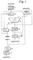
- FIG. 1 is a block diagram of one example of a conventional restoring divider comprising a divisor register (DSR) 1 in which a divisor is stored and the divisor is fed to a multiplier (MULT) 2.
- the multiplier 2 receives a partial quotient predicting signal (hereinafter shown as "m") from a partial quotient predictor (QP) 3 and forms dividends multiplied by -15, -14, -13, ..., -2, -1, 0, . +1, +2, ..., +14, +15 when the radix is 16.
- m partial quotient predicting signal
- the remainder register 6 holds the final predicted remainder for the repetition operation, and after the adding and subtracting operations are repeated, a correct quotient is output via a remainder corrector (RMDC) 7.
- a remainder corrector RMDC 7
- a sign bit of the remainder register (RMD) 6 when a sign bit of the remainder register (RMD) 6 is negative, the complement of 2 is determined as the quotient, and when the sign bit of the remainder register 6 is positive, the value is determined as the quotient.
- a partial quotient generator (QG) 8 compares the output of the partial quotient predicting circuit (QP) 3 and the sign bit of the partial remainder register (PR) 4, so that a correct partial quotient is determined and stored in a quotient register (QR) 9.
- the partial quotient predicting circuit (QP) 3 calculates the value of m in m x DSR to be calculated next from the output of the carry propagate adder (CPA) 5 (hereinafter referred to as CPA) and the output of the divisor register (DSR) 1 (hereinafter referred to as DSR). Logically, the circuit (QP) 3 uses the entries in the above-mentioned CPA and DSR to retrieve the table for m.
- CPA carry propagate adder
- DSR divisor register
- the CPA and m are used as the entry, and the DSR table is formed, in such a manner that the table is reversely retrieved.
- m becomes 5 bits including the sign
- CPA becomes 6 bits including the sign
- the size of the table becomes 64 x 32 entries, so that the size of the table is decreased to about 1/8.
- the adding and subtracting result (CPA) 0,. the table above is almost symmetrical, and the possibility of retrenchment is included.
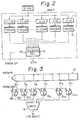
- Figure 2 is a diagram showing the principle of the multiplier shown in Fig. 1.
- 11 designates multiply circuits [x(-15) ⁇ xl5]
- 12 designates divisor registers (-15DSR ⁇ +15DSR)
- 13 designates a selector.
- the radix is 16
- thirty kinds of multiplier registers -15x divisor, -14x divisor, ... , -2x divisor, -lx divisor, 2x divisor, ... , 14x divisor, 15x divisor are necessary.
- Figure 3 is a diagram showing a principle of the partial quotient predicting circuit shown in Fig. 1.
- the six upper bits of the carry propagating adder 5 are supplied to a memory 14 as an address, and in the memory 14, the contents are divided into thirty one groups each having 9 bits, that is D F , D E , ..., D O , D -1 , D -2 ... D -F .
- the divided values D F , D E , ... , D O , D -1 , ... , D -F are supplied to comparators 15 F ... 15 O , ... 15 -F .
- the upper five bits of the divisor (DSR) is supplied to other input terminals of the comparators 15 F ⁇ 15 O .
- the input is formed by a 9 bit signal, the output thereof is a one bit signal.
- the output becomes "I”
- the output becomes "0"
- 16 is a circuit for detecting "1" bit in the left most side.
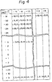
- Figure 4 shows a precise table which receives the CPA and m as entries and designates the DSR.
- the table shown in Fig. 4 has 64 x 31 entries.
- CPAO shows the value at which the upper 6 bits (including the sign) of CPA output are extracted and designates the decimal number
- m is the signal of the partial quotient predicting circuit (QP) 3 designated by the decimal number.
- Such table look up system can be replaced by a random logic circuit which performs the same function.
- the CPAO row m column in the partial quotient predicting table [QPT(CPAO, m)] designates the logical function whereby the upper 9 bits of the DSR (hereinafter referred to as DSRO) are input, and these have the value "1" or "0", (hereinafter, referred to as [LcpaO, m(DSRO)]).
- Fig. 4 The partial quotient predicting table formed by above-mentioned method is shown in Fig. 4.
- Fig. 4 when a DSRO having 9 bits is input, only one m exists for all CPAO (64 bits) and the corresponding logic function is
- the DSRO is 8 bits, only one m exists for all CPAO and the condition: is not satisfied, so that the table does not function as the partial quotient predicting table.
- the DSRO is 10 bits, it becomes redundant since only one m exists for all CPAO. Therefore, when the DSRO is 9 bits, this may be said to be the most suitable number of bits in the DSRO for retrieving m in the nonrestoring divider wherein the radix is 16.
- Figure 5 is a block diagram of one embodiment of the nonrestcring divider apparatus according to the present invention.
- the same symbols correspond to the same elements as shown in Fig. 1.
- an adder 51 adds the upper bits of the partial remainder register (PR) 4 and the upper bits of output of the multiplier (MULT) 2 that is, the upper bits of mDSR without using the carry signal from an adder 52 (the output signal of the carry predicting circuit (CLA) 521), and the output thereof is supplied to a complement generator 10 and the remainder register (RMD) 6.
- the result obtained from the complement generator (COMP) 10 is decoded and supplied to the partial quotient predicting circuit (QP2) 3.
- An adder (ADDER 2) 52 receives the lower bits of the partial remainder register (PR) 4 and the lower bits of the output (mDSR) of the multiplier (MULT) 2, and a carry look-ahead circuit (CLA) 521 is attached thereto for the purpose of carrying out high speed operations.
- ADDER 2 receives the lower bits of the partial remainder register (PR) 4 and the lower bits of the output (mDSR) of the multiplier (MULT) 2, and a carry look-ahead circuit (CLA) 521 is attached thereto for the purpose of carrying out high speed operations.
- the output of the adder 51 is also input to a carry adding circuit 53 and compensated by the output of CLA 521 and fed to RMD6 by being concatinated with the output of adder 52.
- the characteristic feature of the present invention is to provide new functional blocks, that is, a modified decoder circuit (MDEC) 111, a selector (SEL) 12, and a partial quotient predicting circuit (QPl) 31 having the same function as that of the partial quotient predicting circuit (QP) 3 explained in Fig. 1 to Fig. 4.
- MDEC modified decoder circuit
- SEL selector
- QPl partial quotient predicting circuit
- the modified decoder circuit (MDEC) 111 forms, in principle, the decode signal assuming +1 when the sign bit of the adder (ADDER 1) 51 is "0" (positive) and the decode signal assuming -1 when the sign bit of the adder 51 is "1" (negative).
- the selector 12 selects either the partial quotient predicting circuit (QP1) 3 or (QP2) 31 by using the output signal of the carry predicting circuit (CLA) 521.
- the selector 12 selects the partial quotient circuit (QP1) 31, and where the output of the circuit (CLA) 521 is "0" (that is, no carry exists), the partial quotient circuit (QP2) 3 is selected.
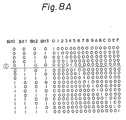
- the function of the modified decoder circuit (MDEC) will be explained in detail later referring to Figs. 8A and 8B.
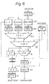
- Figure 6 is a block diagram of another embodiment of the present invention.
- Fig. 6 22 designates multipliers ( ⁇ 1x, +2/+4x, +8/+16x) which are formed by a complement circuit and a shifter, wherein multiplication in the + side is achieved by shift only and multiplication in the - side is achieved by using the complement; 23 designates divisor registers (SR #1, SR #2, SR #3); 24 and 25 carry save adders (CSAl, CSA2) having three inputs; C designates a carry signal; and S designates a sum signal.
- multipliers ⁇ 1x, +2/+4x, +8/+16x
- the divisor registers 23 [corresponding to (+15DSR ⁇ -15 DSR) in Fig. 2] are formed by three registers (SR #1 ⁇ SR #3) the number of which is smaller than the number of bits (4), and the outputs of four registers SR #1, SR #2, SR #3 and the partial remainder register(PR) 4 are added by using two carry/save adders 24, 25 having three inputs.
- the divisor When the divisor is set in the divisor register ( DSR ) 1 and the dividend is set in the partial remainder register (PR) 4, the dividend is supplied via the three-input carry/save adder (CSA 2) 25 to the partial quotient predicting circuit (QP) 3, and a signal predicting the most significant digit of the quotient is output.
- This predicting signal selects a plurality of routes by which the output of the divisor register 1 is multiplied by the adders 22 (+lx, +2/+4x, +8/+16x), and the outputs thereof are set in the divisor registers (SR #1, SR #2, SR #3) 23.
- the outputs of the divisor registers (SR #1, SR #2, SR #3) 23 and the output of the partial remainder register (PR) 4 are added by using the three-input carry/save adders (CSA1, CSA2) 24, 25 and the carry propagation adder 5, and the output thereof is again input to the partial remainder register (PR) 4.
- the output (C, S) of the three-input carry/save adder (CSA2) 25 is supplied to the partial quotient predicting circuit (QP) 3, so as to determine the inputs of the three kinds of divisor registers (SR #1, SR #2, SR #3) which will be selected next.
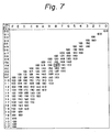
- Fig. 7 is a diagram showing one embodiment of the partial quotient predicting table according to the present invention.
- the value m i is selected so that the value of P i+1 obtained by calculating the equation 1 satisfies the equation 2, and the equation 1 is calculated by using the selected m..
- a method for using the multiplier, a method for using a divisor register at every multiple, a method for using carry/save adders, etc. are well known and the subtraction p i - m i x d is carried out by using a well known adding and subtracting circuit, etc.
- the feature of the present invention lies within the carrying out of the function of determining m i which satisfies the equation 2 from P i and D above by using the smallest possible amount of hardware.
- the set M(P i , D) of m i which satisfies the equations 1, 2 at the i'th step, is a partial set of X, and usually a plurality of elements exist. That is,
- N is specified as the mapping which is mapped from the partial set X and in which the sign of each element is inverted. That is, when then
- the table which determines m i from any P i and D is provided only for P i ⁇ 0, so that the size of the table can be reduced by about one-half.
- the elements of the partial sets M(P i , D), M( P i , D) can be obtained by providing one table of M'(P i , D ).
- Figure 7 shows the table in which the relationship between P i , D, and m i is obtained by using the above-mentioned principle.
- m i is 4 bits
- P i is 5 bits without a sign
- D is 9 bits (however, it is normalized so that the most significant bit becomes "1"), and several discontinuous points exist therebetween.
- a comparative continuous relationship exists, that is, when D increases, m i decreases.
- the process for determining m i logically corresponds to the retrieval of the table which uses P. and D as entries to determine the value of m i .
- P i becomes 6 bits including the sign, a table must be formed having 64 entries x 256 entries, and this is not practical.
- the upper 5 bits of P i are designated as a hexadecimal number
- the 4 bits of m i are designated as a hexadecimal number
- the upper 9 bits (wherein the most significant bit is "1") of D are designated as a hexadecimal number.
- the upper 9 bits of D designates a lower limit value for the elements entry.
- Fig. 8A shows one example of the function of the usual decoder (DEC) 11 shown in Fig. 5 and the function of the modified decoder (MDEC) 111 shown in Fig. 5.
- DEC usual decoder
- MDEC modified decoder
- the output data of the adder 51 is '11011', the sign bit of the data is "1" (negative). Therefore, according to the logic disclosed in the prior Japanese Unexamined Application No. 59-070353, the output of the adder 51, that is the complemental output of "1", is supplied to the decoder circuits 11 and 111, and the absolute value of the partial quotient predicting. signal m is output.
- the output [shown in 1 on Fig. 8A, that is, the decoded output which places the line 4 to an ON state] of the decoder 11 corresponding to the complemental output is supplied to the partial quotient predicting circuit 3.
- the output of the partial quotient predicting circuit 3 includes a carry, the original data becomes '11100' and then it is predicted that the complemental output will become '0011'.
- the selector 12 exerts control through the carry from the carry predicting circuit 521 so that the output of the decode circuit input as '10100' including the sign [shown in 3 on Fig. 7B, that is, the output which places the line 3 to an ON state] is supplied to the modified decoder 111 and the input partial quotient predicting signal is supplied to the partial quotient predicting circuit 31.
- the correct partial quotient predicting signal m is obtained.
- the modified decoder 111 forms the decode signal predicting +1 when the sign bit of the adder 51 is principally “0" positive, and forms the decode signal predicting -1 when the sign bit thereof is "1" (negative).
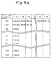
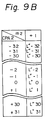
- Figures 9A and 9B are an alternative to the example shown in Fig. 7.
- the CPAO is 6 bits (64 entries), the obtained-m is 5 bits including the sign (32 entries), and the radix is 16.
- m 4 bits including the signal (expressed by ml)
- the table which satisfies the table shown in Fig. 4, (that is, the CONDITION I above) can be obtained.
- This table is a rough portion of quotient predicting table shown in Fig. 9A.
- Figure 9B is a table which schematically shows the above mentioned correcting table.
- the above-mentioned correcting table is formed by the above-mentioned condition, and each element thereof is expressed by the following equation.
- the same function as shown in the precise portion the quotient predicting table shown in Fig. 4 can be realized by the rough portion of the quotient predicting table shown in Fig. 9A and the correcting table shown in Fig. 9B, so that it is recognized that the amount of hardware needed can be decreased.
- CPA and m are used as the entry of the partial quotient predicting table, however, m can be placed to the value coded by using a plurality of desired values from -16 to +15, to form an effective signal in the subsequent process.
Landscapes
- Engineering & Computer Science (AREA)
- Physics & Mathematics (AREA)
- General Physics & Mathematics (AREA)
- Pure & Applied Mathematics (AREA)
- Computational Mathematics (AREA)
- Mathematical Analysis (AREA)
- Mathematical Optimization (AREA)
- Theoretical Computer Science (AREA)
- Computing Systems (AREA)
- General Engineering & Computer Science (AREA)
- Nonlinear Science (AREA)
- Complex Calculations (AREA)
- Error Detection And Correction (AREA)
Abstract
Description
- This invention relates to a nonrestoring divider and, more particularly, to a high speed circuit construction by which a circuit for predicting a partial quotient is formed using a smaller amount of hardware.
- Conventionally, a momrestoring divider is used as one element of a divider system. In such a system, sets of quotients used for forming digits of the quotient are controlled in such a manner that where sets of quotients exist which do not include a zero, then each digit of the quotient is selected therefrom.
- These particular sets of the quotients having no zero are usually expressed as follows, wherein "r" represents the radix.
- -(r - 1), -(r - 2),..., -1, +1, ..., r - 2, r - 1 In many calculators, calculation is carried out by using a plurality of bit units rather than just one bit unit and, obviously, a radix larger than 2 is used.
- For example, the radix is 4 in a 2 bit unit, and becomes 8 in a 3 bit unit.
- Usually, an operation unit of ℓ bits is an m digit figure having r as the radix, and is expressed as; r = 2ℓ/m
- A characteristic feature of nonrestoring division is the use of a negative number in the digits as a result of the operation by remaining the inversion of negative and the positive of the dividend formed when the digit of the result of the operation is determined, and the dividend or multiple of the dividend is added or subtracted by the sign for the dividend by using the negative number in the result of the operation.
- For example, the values multiplying the dividend by k [i.e., the multiple -(= - 1), -(r - 2), ..., -1, +1, ..., r - 2, r - 1] are set in the divisor registers, the divisor registers are selected by a predicting signal output from a partial quotient predictor, and the quotient is obtained by repeatedly adding and subtracting the values multiplying the dividend by k.
- In such a nonrestoring divider system, when the number of bits "n" used as the operation unit becomes large, the radix is increased, for example to 2n, so that the number of operation repetitions can be decreased and high speed operation can be expected. However, the multiplying of the divisor becomes complex, and therefore the predicting logic for the quotient must be precise, which gives rise to the problem that the number of circuits must be considerably increased.
- Concerning the logic for predicting the partial quotient, a method has not been developed for forming an effective predicting circuit for the partial quotient.
- An object of the present invention is to provide a nonrestoring divider which can decrease the time needed for predicting the partial quotient.
- Another object of the present invention is to provide a nonrestoring divider which can decrease the amount of hardware used for the logic needed for predicting the partial quotient.
- According to the invention there is provided a divider apparatus which includes a divisor register for setting a divisor; a partial remainder register for setting a dividend or a partial remainder; a predictor for predicting a partial quotient; a multiplier for multiplying the content of the divisor register; a first adder for subtracting the output of the multiplier from the content of the partial remainder register and for calculating the partial remainder, so that the predictor predicts the partial quotient from upper digits of the divisor register and upper digits of the partial remainder, and also repeats a cycle which sets the output of the adder at the partial remainder register so as to carry out the division, characterised by a second adder for determining the difference between the upper digits of the multiplier and the upper digits of the partial remainder register, a first predictor for predicting the partial quotient from the output of the second adder and the upper digits of the divisor register; a second predictor for predicting the partial quotient from a corrected output of the second adder and the upper digits of the divisor register; first means for determining a carry to be propagated to the second adder from the remainder digits of the multiplier and the remainder digits of the partial remainder register; and second means for selecting either the output of the first predictor or the output of the second predictor by using the output of the first means, thereby making the output of the second means correspond to a predicted quotient.
- Embodiments of the invention will now be described, by way of example, with reference to the accompanying drawings, in which
- Figure 1 is a diagram showing the principle of one example of a conventional nonrestoring divider apparatus;
- Figure 2 is a diagram showing the principle of one example of a multiplier shown in Figure 1;
- Figure 3 is a diagram showing the principle of one example of a circuit for predicting a partial quotient shown in Figure 1;
- Figure 4 is a diagram showing the content of the circuit for predicting a partial quotient;
- Figure 5 is a block diagram of one embodiment of a nonrestoring divider apparatus according to the present invention;
- Figure 6 is a diagram showing an improvement of the mutiplier shown in Figure 5;
- Figure 7 is a diagram showing the content of the circuit for predicting a partial quotient shown in Figure 5;
- Figures 8A and 8B are diagrams showing the logic states of the decoder shown in Figure 5; and
- Figures 9A and 9B are diagrams showing another embodiment of the content shown in Figure 7.
- Figure 1 is a block diagram of one example of a conventional restoring divider comprising a divisor register (DSR) 1 in which a divisor is stored and the divisor is fed to a multiplier (MULT) 2. The
multiplier 2 receives a partial quotient predicting signal (hereinafter shown as "m") from a partial quotient predictor (QP) 3 and forms dividends multiplied by -15, -14, -13, ..., -2, -1, 0,. +1, +2, ..., +14, +15 when the radix is 16. Note, in this circuit a method in which whole multiples are previously formed and selected, a method which uses a general adder, or a method which calculates by using a smaller number of divisor registers than the radix and multi-stage carry/save adders can be used. - In a partial remainder register (PR) 4, after the dividend is set at the first operation cycle, a new partial remainder is set at every operation cycle. A carry propagate adder (CPA) 5 carries out the addition of -the
partial remainder register 4 and a divisor multiplied by m (-15 = m ≦ +15: where m is an integer), and the result thereof is output to thepartial quotient register 4, thepartial quotient predictor 3, and aremainder register 6. - The
remainder register 6 holds the final predicted remainder for the repetition operation, and after the adding and subtracting operations are repeated, a correct quotient is output via a remainder corrector (RMDC) 7. In a concrete correcting method in the remainder corrector (RMDC) 7, when a sign bit of the remainder register (RMD) 6 is negative, the complement of 2 is determined as the quotient, and when the sign bit of theremainder register 6 is positive, the value is determined as the quotient. - A partial quotient generator (QG) 8 compares the output of the partial quotient predicting circuit (QP) 3 and the sign bit of the partial remainder register (PR) 4, so that a correct partial quotient is determined and stored in a quotient register (QR) 9.
- The partial quotient predicting circuit (QP) 3, according to the present invention, calculates the value of m in m x DSR to be calculated next from the output of the carry propagate adder (CPA) 5 (hereinafter referred to as CPA) and the output of the divisor register (DSR) 1 (hereinafter referred to as DSR). Logically, the circuit (QP) 3 uses the entries in the above-mentioned CPA and DSR to retrieve the table for m.
- However, when the CPA and DSR are used in this way, the table is extremely large. For example, in the nonrestoring dividing operation having a radix of 16, including the sign bit, the following table will be formed:
- CPA: 6 bits (64 entries)
- DSR: 9 bits (256 entries)
- Therefore, in practice, the CPA and m are used as the entry, and the DSR table is formed, in such a manner that the table is reversely retrieved. In the table mentioned above, m becomes 5 bits including the sign, CPA becomes 6 bits including the sign, and as mentioned above, the size of the table becomes 64 x 32 entries, so that the size of the table is decreased to about 1/8. Referring to the adding and subtracting result (CPA) = 0,. the table above is almost symmetrical, and the possibility of retrenchment is included.
- Figure 2 is a diagram showing the principle of the multiplier shown in Fig. 1. In Fig. 2, 11 designates multiply circuits [x(-15) ~ xl5], 12 designates divisor registers (-15DSR ~ +15DSR), and 13 designates a selector. In the conventional system, when the radix is 16, thirty kinds of multiplier registers -15x divisor, -14x divisor, ... , -2x divisor, -lx divisor, 2x divisor, ... , 14x divisor, 15x divisor are necessary. These thirty kinds of data are formed by the multiply circuits [x(-15), ..., x15] 11, the outputs are held in the divisor registers (-15DSR ~ +15DSR) 12, and the outputs of the
divisor registers 12 are supplied to theselectors 13. In theselector 13, the values held in theregisters 12 are selected by the signal m, that is, one of the multiple thirty kinds of data is selected. - Figure 3 is a diagram showing a principle of the partial quotient predicting circuit shown in Fig. 1. In Fig. 3, the six upper bits of the
carry propagating adder 5 are supplied to amemory 14 as an address, and in thememory 14, the contents are divided into thirty one groups each having 9 bits, that is DF, DE, ..., DO, D-1, D-2 ... D-F. The divided values DF, DE, ... , DO, D-1, ... , D-F are supplied tocomparators 15F ... 15O, ... 15-F. Further, the upper five bits of the divisor (DSR) is supplied to other input terminals of thecomparators 15F ~ 15O. In thecomparators 15F ~ 15O, the input is formed by a 9 bit signal, the output thereof is a one bit signal. When the inputs have the relationship A > B, the output becomes "I", and when the inputs have the relationship A < B, the output becomes "0". In Fig. 3, 16 is a circuit for detecting "1" bit in the left most side. - Figure 4 shows a precise table which receives the CPA and m as entries and designates the DSR. The table shown in Fig. 4 has 64 x 31 entries. In Fig. 4, CPAO shows the value at which the upper 6 bits (including the sign) of CPA output are extracted and designates the decimal number, and m is the signal of the partial quotient predicting circuit (QP) 3 designated by the decimal number.
- Such table look up system can be replaced by a random logic circuit which performs the same function.
- The CPAO row m column in the partial quotient predicting table [QPT(CPAO, m)] designates the logical function whereby the upper 9 bits of the DSR (hereinafter referred to as DSRO) are input, and these have the value "1" or "0", (hereinafter, referred to as [LcpaO, m(DSRO)]).
- For the purpose of simplifying the explanation, it is assumed that the DSR is normalized so that it is a positive integer and the most significant bit becomes 1.
- First, the principle of the nonrestoring divider will be explained. When the divisor is D, the dividend is Pn, the partial remainder is Pn, and the partial remainder predicting signal is m; then the dividing operation in the nonrestoring divider is expressed by the following asymptotic equation,


- ① This logic function "LcpaO, m(DSRO)" becomes 1 when the dividing condition


- and this function becomes 0, except for the above,
- ② When the following relationship exists between m and m'

- ③ The condition wherein the partial quotient predicting table formed by using the process mentioned above functions is that where one m exists for all CPAO, DSRO, and the following equation is satisfied for such an m

- The partial quotient predicting table formed by above-mentioned method is shown in Fig. 4. In Fig. 4, when a DSRO having 9 bits is input, only one m exists for all CPAO (64 bits) and the corresponding logic function is

- If the DSRO is 8 bits, only one m exists for all CPAO and the condition:

- Further, if the DSRO is 10 bits, it becomes redundant since only one m exists for all CPAO. Therefore, when the DSRO is 9 bits, this may be said to be the most suitable number of bits in the DSRO for retrieving m in the nonrestoring divider wherein the radix is 16.
- Figure 5 is a block diagram of one embodiment of the nonrestcring divider apparatus according to the present invention. In Fig. 5, the same symbols correspond to the same elements as shown in Fig. 1.
- In Fig. 5, an
adder 51 adds the upper bits of the partial remainder register (PR) 4 and the upper bits of output of the multiplier (MULT) 2 that is, the upper bits of mDSR without using the carry signal from an adder 52 (the output signal of the carry predicting circuit (CLA) 521), and the output thereof is supplied to acomplement generator 10 and the remainder register (RMD) 6. - In the
complement generator 10, when the sign bit of the adder (ADDER 1) 51 is "1", the complement of the input data (output of the adder 51) is output to thedecoder 11, and when the sign bit is "0", the input data is directly output to thedecoder 11. - In the -
decoder 11, the result obtained from the complement generator (COMP) 10 is decoded and supplied to the partial quotient predicting circuit (QP2) 3. - An adder (ADDER 2) 52 receives the lower bits of the partial remainder register (PR) 4 and the lower bits of the output (mDSR) of the multiplier (MULT) 2, and a carry look-ahead circuit (CLA) 521 is attached thereto for the purpose of carrying out high speed operations.
- The output of the
adder 51 is also input to acarry adding circuit 53 and compensated by the output ofCLA 521 and fed to RMD6 by being concatinated with the output ofadder 52. - The characteristic feature of the present invention is to provide new functional blocks, that is, a modified decoder circuit (MDEC) 111, a selector (SEL) 12, and a partial quotient predicting circuit (QPl) 31 having the same function as that of the partial quotient predicting circuit (QP) 3 explained in Fig. 1 to Fig. 4.
- The basic operation of the apparatus shown in Fig. 5 is similar to the conventional system, therefore, only the characteristic feature of the present invention will be explained hereinafter.
- First, the modified decoder circuit (MDEC) 111 forms, in principle, the decode signal assuming +1 when the sign bit of the adder (ADDER 1) 51 is "0" (positive) and the decode signal assuming -1 when the sign bit of the
adder 51 is "1" (negative). Theselector 12 selects either the partial quotient predicting circuit (QP1) 3 or (QP2) 31 by using the output signal of the carry predicting circuit (CLA) 521. - Concretely, when the output of the carry predicting circuit (CLA) 521 is "1" (that is, a carry exists), the
selector 12 selects the partial quotient circuit (QP1) 31, and where the output of the circuit (CLA) 521 is "0" (that is, no carry exists), the partial quotient circuit (QP2) 3 is selected. The function of the modified decoder circuit (MDEC) will be explained in detail later referring to Figs. 8A and 8B. - Figure 6 is a block diagram of another embodiment of the present invention.
- In Fig. 6, 22 designates multipliers (±1x, +2/+4x, +8/+16x) which are formed by a complement circuit and a shifter, wherein multiplication in the + side is achieved by shift only and multiplication in the - side is achieved by using the complement; 23 designates divisor registers (
SR # 1,SR # 2, SR #3); 24 and 25 carry save adders (CSAl, CSA2) having three inputs; C designates a carry signal; and S designates a sum signal. - In the circuit shown in Fig. 6, the divisor registers 23 [corresponding to (+15DSR ~ -15 DSR) in Fig. 2] are formed by three registers (
SR # 1 ~ SR #3) the number of which is smaller than the number of bits (4), and the outputs of fourregisters SR # 1,SR # 2,SR # 3 and the partial remainder register(PR) 4 are added by using two carry/saveadders - When the divisor is set in the divisor register (DSR) 1 and the dividend is set in the partial remainder register (PR) 4, the dividend is supplied via the three-input carry/save adder (CSA 2) 25 to the partial quotient predicting circuit (QP) 3, and a signal predicting the most significant digit of the quotient is output. This predicting signal selects a plurality of routes by which the output of the
divisor register 1 is multiplied by the adders 22 (+lx, +2/+4x, +8/+16x), and the outputs thereof are set in the divisor registers (SR # 1,SR # 2, SR #3) 23. - Next, the outputs of the divisor registers (
SR # 1,SR # 2, SR #3) 23 and the output of the partial remainder register (PR) 4 are added by using the three-input carry/save adders (CSA1, CSA2) 24, 25 and thecarry propagation adder 5, and the output thereof is again input to the partial remainder register (PR) 4. - The output (C, S) of the three-input carry/save adder (CSA2) 25 is supplied to the partial quotient predicting circuit (QP) 3, so as to determine the inputs of the three kinds of divisor registers (
SR # 1,SR # 2, SR #3) which will be selected next. - Fig. 7 is a diagram showing one embodiment of the partial quotient predicting table according to the present invention.
- First, the concept of the present invention will be explained. At the i'th step of the non-restoring division, the following equations are used.


- The value mi is selected so that the value of Pi+1 obtained by calculating the
equation ① satisfies theequation ②, and theequation ① is calculated by using the selected m.. - In the actual computer, at the best case, the upper bits of pi and d [corresponded to Pi in CPA and D in DSR] are extracted by digits sufficient to ensure accuracy in determining mi, the value of mi is - determined by using the partial quotient predicting table, and thereafter precise Pi+1 is calculated by using
equation ①. - As an operation for mi x d, a method for using the multiplier, a method for using a divisor register at every multiple, a method for using carry/save adders, etc., are well known and the subtraction pi - mi x d is carried out by using a well known adding and subtracting circuit, etc.
- The feature of the present invention lies within the carrying out of the function of determining mi which satisfies the
equation ② from Pi and D above by using the smallest possible amount of hardware. - As mentioned above, when P. , D are fixed, a plurality values of mi exist which satisfy the
equations - When the quotient sets in the nonrestoring divider is x [= (-r, -
r + 1, ... , -1, 0, 1, ... , r - 1 , r) wherein r is a radix], the set M(Pi, D) of mi, which satisfies theequations -

- Wherein N is specified as the mapping which is mapped from the partial set X and in which the sign of each element is inverted. That is, when


- When the complement of Pi is shown by
P i, M(Pi, D), N[M(Pi, D) have a common portion, but they are not coincident. That is, generally,


- In other words, when Pi ≧ 0, a suitable mi is determined by selecting one element from M'(Pi , D), and when
P i < 0, a suitable mi is determined by selecting one element from N[M'(Pi, D)]. - Therefore, when the system of the present invention is used, the table which determines mi from any Pi and D is provided only for Pi ≧ 0, so that the size of the table can be reduced by about one-half.
- The above-mentioned will be explained by using the example of the nonrestoring division by which the quotient having 4 bits (that is radix r = 16) is obtained in one cycle time (one step).
- When r = 16, for the purpose of determining m. , Pi requires 6 bits including the sign and D requires 9 bits (however, for the purpose of simplicity, it is previously normalized so that D is positive and the most significant bit is "1").
- Further, the following relationship exists between the accuracies of the P. , D mentioned above. That is, when one is rough, the other requires high accuracy. The above relationship, that is, Pi = 6 bits and D = 9 bits, is one combination relating to that relationship.
- As a concrete example of the Pi and D mentioned above, when


above equations 

- Then, from the definition of the mapping mentioned above, it may be said that


- If, by providing the table of M'(Pi, D), the upper bits Pi of the input Pi are


- Accordingly, in accordance with the definition of the mapping, the following relationship can be obtained:

- To summarize the above-mentioned explanation concerning the concept of the present invention, the following relationship exists between the partial sets M(P. , D) and M(
P i, D) of the quotient set X,


- Therefore, when set as M'(Pi, D)a, it becomes


- Thus, the elements of the partial sets M(Pi, D), M(
P i, D) can be obtained by providing one table of M'(Pi, D). - Figure 7 shows the table in which the relationship between Pi, D, and mi is obtained by using the above-mentioned principle.
- In Fig. 7, mi is 4 bits, Pi is 5 bits without a sign, D is 9 bits (however, it is normalized so that the most significant bit becomes "1"), and several discontinuous points exist therebetween. However, it is known that a comparative continuous relationship exists, that is, when D increases, mi decreases.
- As mentioned above, the process for determining mi logically corresponds to the retrieval of the table which uses P. and D as entries to determine the value of mi. As Pi becomes 6 bits including the sign, a table must be formed having 64 entries x 256 entries, and this is not practical.
- Therefore, it is considered that the construction of the table which uses Pi, mi as entries and the range for D as elements as shown in Fig. 6 is the most efficient.
- In the table shown in Fig. 7, the upper 5 bits of Pi are designated as a hexadecimal number, the 4 bits of mi are designated as a hexadecimal number, and the upper 9 bits (wherein the most significant bit is "1") of D are designated as a hexadecimal number. The upper 9 bits of D designates a lower limit value for the elements entry.
- Therefore, when the elements of the table are


- As a concrete example, when Pi = '001011' is designated as a hexadecimal number without a sign, it becomes 'OB'(H), and similarly, D = '110000000' becomes '180'(H). Therefore, in the table, as


- it is known that the value to be determined is '8'. When the following relationship is given

- Fig. 8A shows one example of the function of the usual decoder (DEC) 11 shown in Fig. 5 and the function of the modified decoder (MDEC) 111 shown in Fig. 5.
- The example of the operation of the invention by which the partial quotient predicting signal m is output when the output data of the adder 51 [that is, the upper digit of PRi + mDSR] is positive and negative.
- When the output data of the
adder 51 is '00100' the sign bit of the data is "0" (positive). Therefore a carry is not input from thecarry predicting circuit 521, and the output of the decoder 11 [that is the decoded output which makes the line 4 (see Fig. 8A) to an ON state, shown by ① in Fig. 8A] is supplied to the partialquotient predicting circuit 3. When the obtained partial quotient predicting signal has a carry, it is predicted that the above-mentioned data will become '00101' and thesector 12 exerts a control through the carry from thecarry predicting circuit 52 so that the output of the decode circuit input as '00100' including the sign [shown in ② in Fig. 8B, that is, the output which places the line 5 (see Fig. 8B) to an ON state] is supplied to the modifieddecoder 111, and the input partial quotient predicting signal is supplied to the partialquotient predicting circuit 31. Thus, the correct partial quotient predicting signal m is obtained. - When the output data of the
adder 51 is '11011', the sign bit of the data is "1" (negative).. Therefore, according to the logic disclosed in the prior Japanese Unexamined Application No. 59-070353, the output of theadder 51, that is the complemental output of "1", is supplied to thedecoder circuits - Therefore, in this case, if no carry from the
carry predicting circuit 521 exists, the complement of 1 of the data '1011' excepting the sign is '0100'. Then the output [shown in ① on Fig. 8A, that is, the decoded output which places theline 4 to an ON state] of thedecoder 11 corresponding to the complemental output is supplied to the partialquotient predicting circuit 3. When the output of the partialquotient predicting circuit 3 includes a carry, the original data becomes '11100' and then it is predicted that the complemental output will become '0011'. Then theselector 12 exerts control through the carry from thecarry predicting circuit 521 so that the output of the decode circuit input as '10100' including the sign [shown in ③ on Fig. 7B, that is, the output which places theline 3 to an ON state] is supplied to the modifieddecoder 111 and the input partial quotient predicting signal is supplied to the partialquotient predicting circuit 31. Thus, the correct partial quotient predicting signal m is obtained. - As mentioned above, the characteristic feature is that, the modified
decoder 111 forms the decode signal predicting +1 when the sign bit of theadder 51 is principally "0" positive, and forms the decode signal predicting -1 when the sign bit thereof is "1" (negative). - Figures 9A and 9B are an alternative to the example shown in Fig. 7.
- In the table shown in Fig. 4, the CPAO is 6 bits (64 entries), the obtained-m is 5 bits including the sign (32 entries), and the radix is 16. However, also when m is 4 bits including the signal (expressed by ml), δ = (1/2)5 [that is, the table is formed by inputting the upper 6 bits (DSRl) of the DSR] and ε = 2 [the CPA is 4 bits (CPAl) including the sign], the table which satisfies the table shown in Fig. 4, (that is, the CONDITION I above) can be obtained.
- This table is a rough portion of quotient predicting table shown in Fig. 9A.
- When the table is as shown in Fig. 9A and as shown in Fig. 4, the following can be known. That is, even when the portion corresponding to add number m in the precise portion of the partial quotient predicting table shown in Fig. 4 is "1", the value ml smaller by "1" than in the table shown in Fig. 4 is obtained in the table shown in Fig. 9A.
- Therefore, for the purpose of correcting the error in both cases, when "1" exists in the portion for the odd number m in the table shown in Fig. 4, the precise m can be obtained by storing its information as another correcting table and by referring to the same. Figure 9B is a table which schematically shows the above mentioned correcting table.
- Hereinafter, the correcting method will be concretely explained.
- First, referring one column CPA1 = -30 in the rough portion of the quotient predicting table, when, for example,
-


- When the corrected value in the same column is


- Further, when in one column in CPA1 = -30 in the rough portion of the quotient predicting table, for example,


- That is, when L" -30 = 1 in the correcting table, it shows that, in the column corresponding to CPAO = -30 in the precise portion of quotient predicting table shown in Fig. 4, one "1" exists at any portion for the odd number m. This is retrieved from the rough portion of quotient predicting table shown in Fig. 9A, and when as mentioned above,


- This is the gist of the present invention.
- Therefore,


- The above-mentioned correcting table is formed by the above-mentioned condition, and each element thereof is expressed by the following equation.
- L"cpa2, m2(DSR2) = ELcpa2, 2i+l(DSR2) = 1 wherein I shows the logical sum from i = -8 to i = +7, cpa2 is the upper 6 bits including the sign in the output of the carry propagate adder, and DSR2 is the upper 9 bits of the dividend.
- The correcting table formed by the equation showing the condition mentioned above is shown in Fig. 9B.
- According to the present invention, the same function as shown in the precise portion the quotient predicting table shown in Fig. 4 can be realized by the rough portion of the quotient predicting table shown in Fig. 9A and the correcting table shown in Fig. 9B, so that it is recognized that the amount of hardware needed can be decreased.
- In the explanation above, CPA and m are used as the entry of the partial quotient predicting table, however, m can be placed to the value coded by using a plurality of desired values from -16 to +15, to form an effective signal in the subsequent process.
Claims (6)
Applications Claiming Priority (4)
| Application Number | Priority Date | Filing Date | Title |
|---|---|---|---|
| JP59070353A JPS60214037A (en) | 1984-04-09 | 1984-04-09 | High cardinal number nonrecovery type divider |
| JP70353/84 | 1984-04-09 | ||
| JP128610/84 | 1984-06-22 | ||
| JP59128610A JPS617939A (en) | 1984-06-22 | 1984-06-22 | High cardinal number non-recovery type dividing device |
Publications (3)
| Publication Number | Publication Date |
|---|---|
| EP0158530A2 true EP0158530A2 (en) | 1985-10-16 |
| EP0158530A3 EP0158530A3 (en) | 1987-12-09 |
| EP0158530B1 EP0158530B1 (en) | 1992-02-05 |
Family
ID=26411512
Family Applications (1)
| Application Number | Title | Priority Date | Filing Date |
|---|---|---|---|
| EP85302455A Expired - Lifetime EP0158530B1 (en) | 1984-04-09 | 1985-04-04 | Nonrestoring divider |
Country Status (8)
| Country | Link |
|---|---|
| US (1) | US4722069A (en) |
| EP (1) | EP0158530B1 (en) |
| KR (1) | KR890003321B1 (en) |
| AU (1) | AU553078B2 (en) |
| BR (1) | BR8501629A (en) |
| CA (1) | CA1231455A (en) |
| DE (1) | DE3585334D1 (en) |
| ES (1) | ES8609768A1 (en) |
Cited By (7)
| Publication number | Priority date | Publication date | Assignee | Title |
|---|---|---|---|---|
| EP0416153A1 (en) * | 1989-09-07 | 1991-03-13 | Siemens Nixdorf Informationssysteme Aktiengesellschaft | Method for dividing any-length operands respectively normalized at the beginning for data processing equipment and digital divider for carrying out the method |
| GB2239536A (en) * | 1989-11-15 | 1991-07-03 | United Technologies Corp | Binary division of signed operands |
| EP0436905A2 (en) * | 1990-01-09 | 1991-07-17 | Digital Equipment Corporation | High performance adder using carry predictions |
| EP0452099A2 (en) * | 1990-04-10 | 1991-10-16 | Matsushita Electric Industrial Co., Ltd. | Divider unit |
| DE4121106A1 (en) * | 1991-06-26 | 1993-01-07 | Siemens Nixdorf Inf Syst | Radix division of binary numbers in data processing system - subjecting divisor to reduction process followed by comparison process to generate part quotients |
| EP0529101A1 (en) * | 1991-03-13 | 1993-03-03 | Fujitsu Limited | Floating-point dividing circuit |
| EP0562137A1 (en) * | 1992-03-24 | 1993-09-29 | Siemens Nixdorf Informationssysteme Aktiengesellschaft | Method for dividing normalized operands |
Families Citing this family (22)
| Publication number | Priority date | Publication date | Assignee | Title |
|---|---|---|---|---|
| US4939686A (en) * | 1987-05-18 | 1990-07-03 | Weitek Corporation | Method and apparatus for shared radix 4 division and radix 4 square root |
| JPH0786826B2 (en) * | 1988-07-19 | 1995-09-20 | 日本電気株式会社 | Integer division circuit |
| US5132925A (en) * | 1988-08-18 | 1992-07-21 | Digital Equipment Corporation | Radix-16 divider using overlapped quotient bit selection and concurrent quotient rounding and correction |
| US5023827A (en) * | 1988-08-18 | 1991-06-11 | Digital Equipment Corporation | Radix-16 divider using overlapped quotient bit selection and concurrent quotient rounding and correction |
| US4992968A (en) * | 1989-02-17 | 1991-02-12 | Digital Equipment Corporation | Division method and apparatus including use of a Z--Z plot to select acceptable quotient bits |
| US4996660A (en) * | 1989-04-17 | 1991-02-26 | International Business Machines Corporation | Selection of divisor multipliers in a floating point divide circuit |
| US5103420A (en) * | 1989-12-04 | 1992-04-07 | Dror Avnon | Method and apparatus for srt division using gray coded quotient bit signals |
| US5128891A (en) * | 1990-04-02 | 1992-07-07 | Advanced Micro Devices, Inc. | High speed divider with square root capability |
| KR920006322B1 (en) * | 1990-04-03 | 1992-08-03 | 정호선 | Divider |
| KR920009092B1 (en) * | 1990-04-03 | 1992-10-13 | 정호선 | Divider circuit |
| US5031138A (en) * | 1990-06-04 | 1991-07-09 | International Business Machines Corporation | Improved ratio decoder for use in a non-restoring binary division circuit |
| JP2835153B2 (en) * | 1990-06-25 | 1998-12-14 | 株式会社東芝 | High radix divider |
| JPH04172526A (en) * | 1990-11-07 | 1992-06-19 | Toshiba Corp | Floating point divider |
| JPH0731592B2 (en) * | 1990-11-29 | 1995-04-10 | 株式会社東芝 | Division circuit |
| JP2502836B2 (en) * | 1991-03-19 | 1996-05-29 | 富士通株式会社 | Preprocessing device for division circuit |
| JP3391448B2 (en) * | 1991-06-07 | 2003-03-31 | 富士通株式会社 | Divider |
| US5381380A (en) * | 1992-05-18 | 1995-01-10 | Sharp Kabushiki Kaisha | Divide circuit having high-speed operating capability |
| US5239498A (en) * | 1992-08-31 | 1993-08-24 | Intel Corporation | Methods and apparatus for improved quotient correction in nonrestoring division computation circuits |
| US6108723A (en) * | 1998-07-20 | 2000-08-22 | Hewlett-Packard Company | System for implementing hardware automated control of burst mode data transfer over a communication link between devices operating in a block mode |
| US7149767B2 (en) * | 2003-05-12 | 2006-12-12 | International Business Machines Corporation | Method and system for determining quotient digits for decimal division in a superscaler processor |
| US8140608B1 (en) * | 2007-05-31 | 2012-03-20 | Nvidia Corporation | Pipelined integer division using floating-point reciprocal |
| JP5169760B2 (en) * | 2008-01-28 | 2013-03-27 | 富士通株式会社 | Communication device, reception data size check method, multiple determination circuit, and multiple determination method |
Citations (3)
| Publication number | Priority date | Publication date | Assignee | Title |
|---|---|---|---|---|
| US3852581A (en) * | 1972-12-14 | 1974-12-03 | Burroughs Corp | Two bit binary divider |
| JPS56123038A (en) * | 1980-03-04 | 1981-09-26 | Fujitsu Ltd | Division control system |
| JPS58142441A (en) * | 1982-02-18 | 1983-08-24 | Toshiba Corp | High radix division system |
Family Cites Families (1)
| Publication number | Priority date | Publication date | Assignee | Title |
|---|---|---|---|---|
| US4320464A (en) * | 1980-05-05 | 1982-03-16 | Control Data Corporation | Binary divider with carry-save adders |
-
1985
- 1985-03-29 CA CA000477910A patent/CA1231455A/en not_active Expired
- 1985-04-02 US US06/719,014 patent/US4722069A/en not_active Expired - Lifetime
- 1985-04-02 AU AU40738/85A patent/AU553078B2/en not_active Ceased
- 1985-04-04 EP EP85302455A patent/EP0158530B1/en not_active Expired - Lifetime
- 1985-04-04 DE DE8585302455T patent/DE3585334D1/en not_active Expired - Fee Related
- 1985-04-08 ES ES542032A patent/ES8609768A1/en not_active Expired
- 1985-04-08 BR BR8501629A patent/BR8501629A/en not_active IP Right Cessation
- 1985-04-09 KR KR8502374A patent/KR890003321B1/en not_active IP Right Cessation
Patent Citations (3)
| Publication number | Priority date | Publication date | Assignee | Title |
|---|---|---|---|---|
| US3852581A (en) * | 1972-12-14 | 1974-12-03 | Burroughs Corp | Two bit binary divider |
| JPS56123038A (en) * | 1980-03-04 | 1981-09-26 | Fujitsu Ltd | Division control system |
| JPS58142441A (en) * | 1982-02-18 | 1983-08-24 | Toshiba Corp | High radix division system |
Non-Patent Citations (3)
| Title |
|---|
| IBM TECHNICAL DISCLOSURE BULLETIN, vol. 24, no. 11B, April 1982, pages 5812-5819, New York, US; K.G. TAN: "Transformed high-radix division for high performance computers" * |
| PATENT ABSTRACTS OF JAPAN, vol. 5, no. 201 (P-94)[873], 19th December 1981; & JP-A-56 123 038 (FUJITSU K.K.) 26-09-1981 * |
| PATENT ABSTRACTS OF JAPAN, vol. 7, no. 260 (P-237)[1405], 18th November 1983; & JP-A-58 142 441 (TOKYO SHIBAURA DENKI K.K.) 24-08-1983 * |
Cited By (12)
| Publication number | Priority date | Publication date | Assignee | Title |
|---|---|---|---|---|
| EP0416153A1 (en) * | 1989-09-07 | 1991-03-13 | Siemens Nixdorf Informationssysteme Aktiengesellschaft | Method for dividing any-length operands respectively normalized at the beginning for data processing equipment and digital divider for carrying out the method |
| GB2239536A (en) * | 1989-11-15 | 1991-07-03 | United Technologies Corp | Binary division of signed operands |
| GB2239536B (en) * | 1989-11-15 | 1994-05-11 | United Technologies Corp | Binary division of signed operands |
| EP0436905A2 (en) * | 1990-01-09 | 1991-07-17 | Digital Equipment Corporation | High performance adder using carry predictions |
| EP0436905A3 (en) * | 1990-01-09 | 1991-11-06 | Digital Equipment Corporation | High performance adder using carry predictions |
| EP0452099A2 (en) * | 1990-04-10 | 1991-10-16 | Matsushita Electric Industrial Co., Ltd. | Divider unit |
| EP0452099A3 (en) * | 1990-04-10 | 1993-06-09 | Matsushita Electric Industrial Co., Ltd. | Divider unit |
| EP0529101A1 (en) * | 1991-03-13 | 1993-03-03 | Fujitsu Limited | Floating-point dividing circuit |
| EP0529101A4 (en) * | 1991-03-13 | 1993-10-20 | Fujitsu Limited | Floating-point dividing circuit |
| US5309383A (en) * | 1991-03-13 | 1994-05-03 | Fujitsu | Floating-point division circuit |
| DE4121106A1 (en) * | 1991-06-26 | 1993-01-07 | Siemens Nixdorf Inf Syst | Radix division of binary numbers in data processing system - subjecting divisor to reduction process followed by comparison process to generate part quotients |
| EP0562137A1 (en) * | 1992-03-24 | 1993-09-29 | Siemens Nixdorf Informationssysteme Aktiengesellschaft | Method for dividing normalized operands |
Also Published As
| Publication number | Publication date |
|---|---|
| ES8609768A1 (en) | 1986-09-01 |
| AU553078B2 (en) | 1986-07-03 |
| US4722069A (en) | 1988-01-26 |
| EP0158530A3 (en) | 1987-12-09 |
| DE3585334D1 (en) | 1992-03-19 |
| CA1231455A (en) | 1988-01-12 |
| ES542032A0 (en) | 1986-09-01 |
| KR890003321B1 (en) | 1989-09-16 |
| BR8501629A (en) | 1985-12-03 |
| EP0158530B1 (en) | 1992-02-05 |
| KR850007899A (en) | 1985-12-09 |
| AU4073885A (en) | 1985-10-17 |
Similar Documents
| Publication | Publication Date | Title |
|---|---|---|
| EP0158530A2 (en) | Nonrestoring divider | |
| US5500812A (en) | Multiplication circuit having rounding function | |
| US5222037A (en) | Floating-point processor for performing an arithmetic operation on fixed-point part data with high speed rounding of a result | |
| EP0149248A2 (en) | Method and apparatus for division using interpolation approximation | |
| KR20010014992A (en) | Divider and method with high radix | |
| US5184318A (en) | Rectangular array signed digit multiplier | |
| EP0356153B1 (en) | Radix-2**n divider method and apparatus using overlapped quotient bit selection and concurrent quotient rounding and correction | |
| KR19990013698A (en) | Calculation method and device | |
| US5132925A (en) | Radix-16 divider using overlapped quotient bit selection and concurrent quotient rounding and correction | |
| KR100203468B1 (en) | Arithmetic apparatus for floating point numbers | |
| US4495593A (en) | Multiple bit encoding technique for combinational multipliers | |
| US5537345A (en) | Mathematical function processor utilizing table information | |
| EP0416308A2 (en) | Rectangular array signed digit multiplier | |
| EP0398568A2 (en) | Multiplier circuit | |
| US5726926A (en) | Shifter for shifting floating point number utilizing arithmetic operation of redundant binary number, and adder containing the same | |
| US5910910A (en) | Circuit and method for rapid calculation of quotients and square roots | |
| EP0366155B1 (en) | Logarithmic function arithmetic unit including means for separately processing pseudo division and multiplication | |
| US4677583A (en) | Apparatus for decimal multiplication | |
| US7016930B2 (en) | Apparatus and method for performing operations implemented by iterative execution of a recurrence equation | |
| US4785412A (en) | Double precision approximate quotient network | |
| US5365471A (en) | Divider for performing signed division using a redundant signed digit | |
| US4118786A (en) | Integrated binary-BCD look-ahead adder | |
| US4823300A (en) | Performing binary multiplication using minimal path algorithm | |
| KR100329914B1 (en) | Dissipation device | |
| US5206826A (en) | Floating-point division cell |
Legal Events
| Date | Code | Title | Description |
|---|---|---|---|
| PUAI | Public reference made under article 153(3) epc to a published international application that has entered the european phase |
Free format text: ORIGINAL CODE: 0009012 |
|
| AK | Designated contracting states |
Designated state(s): DE FR GB |
|
| PUAL | Search report despatched |
Free format text: ORIGINAL CODE: 0009013 |
|
| RHK1 | Main classification (correction) |
Ipc: G06F 7/52 |
|
| AK | Designated contracting states |
Kind code of ref document: A3 Designated state(s): DE FR GB |
|
| 17P | Request for examination filed |
Effective date: 19880527 |
|
| 17Q | First examination report despatched |
Effective date: 19891127 |
|
| GRAA | (expected) grant |
Free format text: ORIGINAL CODE: 0009210 |
|
| AK | Designated contracting states |
Kind code of ref document: B1 Designated state(s): DE FR GB |
|
| REF | Corresponds to: |
Ref document number: 3585334 Country of ref document: DE Date of ref document: 19920319 |
|
| ET | Fr: translation filed | ||
| PLBE | No opposition filed within time limit |
Free format text: ORIGINAL CODE: 0009261 |
|
| STAA | Information on the status of an ep patent application or granted ep patent |
Free format text: STATUS: NO OPPOSITION FILED WITHIN TIME LIMIT |
|
| 26N | No opposition filed | ||
| PGFP | Annual fee paid to national office [announced via postgrant information from national office to epo] |
Ref country code: GB Payment date: 20000329 Year of fee payment: 16 |
|
| PGFP | Annual fee paid to national office [announced via postgrant information from national office to epo] |
Ref country code: DE Payment date: 20000403 Year of fee payment: 16 |
|
| PGFP | Annual fee paid to national office [announced via postgrant information from national office to epo] |
Ref country code: FR Payment date: 20000411 Year of fee payment: 16 |
|
| PG25 | Lapsed in a contracting state [announced via postgrant information from national office to epo] |
Ref country code: GB Free format text: LAPSE BECAUSE OF NON-PAYMENT OF DUE FEES Effective date: 20010404 |
|
| PG25 | Lapsed in a contracting state [announced via postgrant information from national office to epo] |
Ref country code: FR Free format text: THE PATENT HAS BEEN ANNULLED BY A DECISION OF A NATIONAL AUTHORITY Effective date: 20010430 |
|
| GBPC | Gb: european patent ceased through non-payment of renewal fee |
Effective date: 20010404 |
|
| PG25 | Lapsed in a contracting state [announced via postgrant information from national office to epo] |
Ref country code: DE Free format text: LAPSE BECAUSE OF NON-PAYMENT OF DUE FEES Effective date: 20020201 |
|
| REG | Reference to a national code |
Ref country code: FR Ref legal event code: ST |