EP0155853B1 - Zone fenêtre-miroir dans un laser à semi-conducteur du type VSIS - Google Patents
Zone fenêtre-miroir dans un laser à semi-conducteur du type VSIS Download PDFInfo
- Publication number
- EP0155853B1 EP0155853B1 EP85301977A EP85301977A EP0155853B1 EP 0155853 B1 EP0155853 B1 EP 0155853B1 EP 85301977 A EP85301977 A EP 85301977A EP 85301977 A EP85301977 A EP 85301977A EP 0155853 B1 EP0155853 B1 EP 0155853B1
- Authority
- EP
- European Patent Office
- Prior art keywords
- window
- semiconductor laser
- shaped groove
- stimulated region
- region
- Prior art date
- Legal status (The legal status is an assumption and is not a legal conclusion. Google has not performed a legal analysis and makes no representation as to the accuracy of the status listed.)
- Expired
Links
Images
Classifications
-
- H—ELECTRICITY
- H01—ELECTRIC ELEMENTS
- H01S—DEVICES USING THE PROCESS OF LIGHT AMPLIFICATION BY STIMULATED EMISSION OF RADIATION [LASER] TO AMPLIFY OR GENERATE LIGHT; DEVICES USING STIMULATED EMISSION OF ELECTROMAGNETIC RADIATION IN WAVE RANGES OTHER THAN OPTICAL
- H01S5/00—Semiconductor lasers
- H01S5/10—Construction or shape of the optical resonator, e.g. extended or external cavity, coupled cavities, bent-guide, varying width, thickness or composition of the active region
- H01S5/16—Window-type lasers, i.e. with a region of non-absorbing material between the active region and the reflecting surface
-
- H—ELECTRICITY
- H01—ELECTRIC ELEMENTS
- H01S—DEVICES USING THE PROCESS OF LIGHT AMPLIFICATION BY STIMULATED EMISSION OF RADIATION [LASER] TO AMPLIFY OR GENERATE LIGHT; DEVICES USING STIMULATED EMISSION OF ELECTROMAGNETIC RADIATION IN WAVE RANGES OTHER THAN OPTICAL
- H01S5/00—Semiconductor lasers
- H01S5/20—Structure or shape of the semiconductor body to guide the optical wave ; Confining structures perpendicular to the optical axis, e.g. index or gain guiding, stripe geometry, broad area lasers, gain tailoring, transverse or lateral reflectors, special cladding structures, MQW barrier reflection layers
- H01S5/24—Structure or shape of the semiconductor body to guide the optical wave ; Confining structures perpendicular to the optical axis, e.g. index or gain guiding, stripe geometry, broad area lasers, gain tailoring, transverse or lateral reflectors, special cladding structures, MQW barrier reflection layers having a grooved structure, e.g. V-grooved, crescent active layer in groove, VSIS laser
-
- H—ELECTRICITY
- H01—ELECTRIC ELEMENTS
- H01S—DEVICES USING THE PROCESS OF LIGHT AMPLIFICATION BY STIMULATED EMISSION OF RADIATION [LASER] TO AMPLIFY OR GENERATE LIGHT; DEVICES USING STIMULATED EMISSION OF ELECTROMAGNETIC RADIATION IN WAVE RANGES OTHER THAN OPTICAL
- H01S5/00—Semiconductor lasers
- H01S5/20—Structure or shape of the semiconductor body to guide the optical wave ; Confining structures perpendicular to the optical axis, e.g. index or gain guiding, stripe geometry, broad area lasers, gain tailoring, transverse or lateral reflectors, special cladding structures, MQW barrier reflection layers
- H01S5/22—Structure or shape of the semiconductor body to guide the optical wave ; Confining structures perpendicular to the optical axis, e.g. index or gain guiding, stripe geometry, broad area lasers, gain tailoring, transverse or lateral reflectors, special cladding structures, MQW barrier reflection layers having a ridge or stripe structure
- H01S5/223—Buried stripe structure
- H01S5/2232—Buried stripe structure with inner confining structure between the active layer and the lower electrode
- H01S5/2234—Buried stripe structure with inner confining structure between the active layer and the lower electrode having a structured substrate surface
Definitions
- the present invention relates to a window V-channeled substrate inner stripe (referred to as VSIS hereinafter) laser.
- VSIS window V-channeled substrate inner stripe
- a window VSIS laser is proposed in, for example, our published European Patent Application No. 0095826.
- the conventional window VSIS laser does not show a smooth mode conversion between the window region having a plane active layer, and a stimulated region having a crescent active layer. Therefore, the operational mode is not stable at a high power operation. Furthermore, it is difficult to accurately control the manufacture of the crescent active layer in the normal liquid phase epitaxial method.
- the present invention aims to provide a semiconductor laser which provides a stable operation even at a high power operation, and even when the ambient temperature varies. It also aims to provide a novel window VSIS semiconductor laser structure, which ensures stable manufacturing.
- a window VSIS semiconductor laser having a stimulated region and respective window regions formed at opposite ends of said stimulated region, comprising:
- V-shaped groove formed in said stimulated region characterised in that one edge of said V-shaped groove formed in said stimulated region is aligned with the corresponding edge of said V-shaped groove formed in said window regions, and in that said V-shaped groove formed in said stimulated region is wider than said V-shaped groove formed in said window regions.
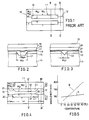
- Figure 1 is a plan view of the conventional window VSIS semiconductor laser.
- Figure 2 shows the structure at the stimulated region, and
- Figure 3 shows the structure at the window region.
- the stripe width W e of a V-shaped groove at a stimulated region 11 is greater than the stripe width W e2 of the V-shaped groove in window regions 12.
- an active layer 17 in the stimulated region has the crescent configuration, and the active layer 17 at the window region has the plane configuration. Further, the active layer 17 in the stimulated region is thicker than the active layer 17 in the window region.
- the thus formed window VSIS semiconductor laser shows the laser emission at the wavelength of 780 nm and at the output power below 120 mW at which the thermal saturation occurs. Further, the window VSIS semiconductor laser of Figure 1 shows a stable fundamental transverse mode below the output power of 60 mW.
- the V-shaped groove is not continuous at a boundary 13 provided between the stimulated region 11 and the window region 12. Therefore, the laser beam is reflected at the boundary 13. That is, a smooth mode conversion is not achieved between the stimulated region 11 and the window region 12. This precludes a stable operation at a high power output operation.
- Figure 4 shows an embodiment of a window VSIS semiconductor laser of the present invention.
- the stimulated region (taken along line II' ⁇ II') has the similar sectional structure as that disclosed in Figure 2.
- the window region taken along line III' ⁇ III' has the similar sectional structure as that disclosed in Figure 3.
- a V-shaped groove C, in the stimulated region 11 has a width W e , which is wider than a width W e2 of a V-shaped groove C 2 in the window regions 12.
- One edge of the V-shaped groove C, in the stimulated region is formed at a position where the edge is aligned on the same line with respect to one edge of the V-shaped groove C 2 formed in the window region 12. Since the stripe width W c1 is wider than the stripe with W. 2 , the remaining edge forms discontinuous boundaries 20 between the stimulated region 11 and the window regions 12.
- Reference numeral 21 refers to a boundary formed between the stimulated region and the window region at the side where the groove edges are aligned, where the waveguide g, of the stimulated region is displaced with respect to the waveguide g 2 of the window region.
- n-GaAs layer 15 (Te-doped concentration 6x10 -18 cm- 3 ) is formed, by the liquid phase epitaxial method, on a p-GaAs substrate 14 (Zn- doped concentration 1x10 -19 cm- 3 ) to have the thickness of about 0.6 microns.
- the V-shaped groove (C 1 C 2 ) having the stripe width W c1 and W c2 is formed in the n-GaAs layer 15 through the use of the photolithography method.
- the stimulated region has a length L e of about 150 microns
- the window region has a length L w of about 50 microns.
- the stripe width W c1 in the stimulated region is preferably about 6 microns, and the stripe width W c2 in the window region is preferably about 3 microns. Therefore, the boundary 20 formed at one edge provided between the stimulated region and the window region has the width of about 3 microns.
- a p-Ga 0.5 Al 0.5 As cladding layer 16, a p-Ga 0.85 Al 0.15 As active layer 17, an n-Ga 0.5 Al 0.5 As cladding layer 18, and an n-GaAs cap layer 19 are sequentially formed on the n-GaAs layer 15 by the liquid phase epitaxial method. That is, the double-hetero structure is formed.
- Each layer 16, 17, 18 and 19 has the thickness of about 0.15 microns, 0.1 microns, 1.0 micron and 2.0 microns, respectively, at the plane portion thereof. Electrodes are formed on both sides, and the laser device is formed by cleaving the semiconductor wafer. A waveguide g, is formed in the stimulated region, and a waveguide g 2 is formed in the window region.
- the one edge of the V-shaped groove is formed continuously between the stimulated region and the window regions, a smooth optical coupling is ensured.
- a stable oscillation in the fundamental mode is conducted even at a high power output. More specifically, the laser emission in the fundamental mode is ensured at the output of 120 mW.
- the waveguides g, and g 2 are slightly discontinuous between the stimulated region and the window regions as shown in Figure 4. Accordingly, the window VSIS semiconductor laser of Figure 4 functions as the inner interference type. Therefore, the transverse mode is very stable.
- Figure 5 shows the variation of the laser wavelength depending on the temperature variation.
- the curve B shows the wavelength variation in the conventional window VSIS semiconductor laser shown in Figure 1, wherein the wavelength varies at the rate of 3 ⁇ / °C.
Landscapes
- Physics & Mathematics (AREA)
- Condensed Matter Physics & Semiconductors (AREA)
- General Physics & Mathematics (AREA)
- Electromagnetism (AREA)
- Optics & Photonics (AREA)
- Geometry (AREA)
- Semiconductor Lasers (AREA)
Claims (5)
caractérisé en ce qu'un bord de la rainure en V (Ci) ménagée dans la région stimulée est aligné avec le bord correspondant de la rainure en V (C2) ménagée dans les régions de fenêtre et en ce que la rainure en V (C1) ménagée dans la région stimulée est plus large que la rainure en V (C2) ménagée dans les régions de fenêtre.
Applications Claiming Priority (4)
| Application Number | Priority Date | Filing Date | Title |
|---|---|---|---|
| JP5504984A JPS60198795A (ja) | 1984-03-21 | 1984-03-21 | 半導体レ−ザ素子 |
| JP5504884A JPS60198794A (ja) | 1984-03-21 | 1984-03-21 | 半導体レ−ザ素子 |
| JP55049/84 | 1984-03-21 | ||
| JP55048/84 | 1984-03-21 |
Related Child Applications (1)
| Application Number | Title | Priority Date | Filing Date |
|---|---|---|---|
| EP90107944A Division-Into EP0387920B1 (fr) | 1984-03-21 | 1985-03-21 | Laser à semi-conducteur du type VSIS avec zone fenêtre-miroir |
Publications (3)
| Publication Number | Publication Date |
|---|---|
| EP0155853A2 EP0155853A2 (fr) | 1985-09-25 |
| EP0155853A3 EP0155853A3 (en) | 1986-12-30 |
| EP0155853B1 true EP0155853B1 (fr) | 1991-01-09 |
Family
ID=26395894
Family Applications (2)
| Application Number | Title | Priority Date | Filing Date |
|---|---|---|---|
| EP90107944A Expired - Lifetime EP0387920B1 (fr) | 1984-03-21 | 1985-03-21 | Laser à semi-conducteur du type VSIS avec zone fenêtre-miroir |
| EP85301977A Expired EP0155853B1 (fr) | 1984-03-21 | 1985-03-21 | Zone fenêtre-miroir dans un laser à semi-conducteur du type VSIS |
Family Applications Before (1)
| Application Number | Title | Priority Date | Filing Date |
|---|---|---|---|
| EP90107944A Expired - Lifetime EP0387920B1 (fr) | 1984-03-21 | 1985-03-21 | Laser à semi-conducteur du type VSIS avec zone fenêtre-miroir |
Country Status (3)
| Country | Link |
|---|---|
| US (1) | US4686679A (fr) |
| EP (2) | EP0387920B1 (fr) |
| DE (2) | DE3581224D1 (fr) |
Families Citing this family (7)
| Publication number | Priority date | Publication date | Assignee | Title |
|---|---|---|---|---|
| JPS6218783A (ja) * | 1985-07-17 | 1987-01-27 | Sharp Corp | 半導体レ−ザ素子 |
| US5087587A (en) * | 1986-02-13 | 1992-02-11 | Sharp Kabushiki Kaisha | Epitaxial growth process for the production of a window semiconductor laser |
| US4764934A (en) * | 1987-07-27 | 1988-08-16 | Ortel Corporation | Superluminescent diode and single mode laser |
| US4843611A (en) * | 1987-07-27 | 1989-06-27 | Ortel Corporation | Superluminescent diode and single mode laser |
| JP3510305B2 (ja) * | 1994-02-22 | 2004-03-29 | 三菱電機株式会社 | 半導体レーザの製造方法,及び半導体レーザ |
| JP2011124253A (ja) * | 2009-12-08 | 2011-06-23 | Sony Corp | 半導体レーザの製造方法、半導体レーザ、光ディスク装置、半導体装置の製造方法および半導体装置 |
| TWI623337B (zh) * | 2015-12-24 | 2018-05-11 | 遠東科技大學 | 可攜式急難救助裝置 |
Family Cites Families (5)
| Publication number | Priority date | Publication date | Assignee | Title |
|---|---|---|---|---|
| US4416011A (en) * | 1981-07-06 | 1983-11-15 | Rca Corporation | Semiconductor light emitting device |
| EP0095826B1 (fr) * | 1982-05-28 | 1988-06-01 | Sharp Kabushiki Kaisha | Laser à semi-conducteur |
| US4546481A (en) * | 1982-05-28 | 1985-10-08 | Sharp Kabushiki Kaisha | Window structure semiconductor laser |
| JPS5961982A (ja) * | 1982-09-30 | 1984-04-09 | Sony Corp | 半導体レ−ザ− |
| US4594718A (en) * | 1983-02-01 | 1986-06-10 | Xerox Corporation | Combination index/gain guided semiconductor lasers |
-
1985
- 1985-03-20 US US06/713,832 patent/US4686679A/en not_active Expired - Fee Related
- 1985-03-21 EP EP90107944A patent/EP0387920B1/fr not_active Expired - Lifetime
- 1985-03-21 EP EP85301977A patent/EP0155853B1/fr not_active Expired
- 1985-03-21 DE DE8585301977T patent/DE3581224D1/de not_active Expired - Lifetime
- 1985-03-21 DE DE90107944T patent/DE3587619T2/de not_active Expired - Fee Related
Also Published As
| Publication number | Publication date |
|---|---|
| EP0155853A3 (en) | 1986-12-30 |
| EP0387920A3 (en) | 1990-12-19 |
| DE3581224D1 (de) | 1991-02-14 |
| DE3587619T2 (de) | 1994-02-24 |
| EP0155853A2 (fr) | 1985-09-25 |
| DE3587619D1 (de) | 1993-11-11 |
| EP0387920B1 (fr) | 1993-10-06 |
| US4686679A (en) | 1987-08-11 |
| EP0387920A2 (fr) | 1990-09-19 |
Similar Documents
| Publication | Publication Date | Title |
|---|---|---|
| EP0064339B1 (fr) | Laser sémiconducteur | |
| US4329660A (en) | Semiconductor light emitting device | |
| EP0095826B1 (fr) | Laser à semi-conducteur | |
| US4803691A (en) | Lateral superradiance suppressing diode laser bar | |
| US5541950A (en) | Semiconductor laser including groove having variable dimensions | |
| EP0104712B1 (fr) | Laser à semi-conducteur | |
| US4788689A (en) | Composite resonator-type semiconductor laser device | |
| EP0155853B1 (fr) | Zone fenêtre-miroir dans un laser à semi-conducteur du type VSIS | |
| US4546481A (en) | Window structure semiconductor laser | |
| US4745615A (en) | Semiconductor laser device with a diffraction grating | |
| EP0194894B1 (fr) | Laser à semi-conducteur | |
| CA1241101A (fr) | Laser a semiconducteur comportant une region passive non absorbante guidant le faisceau | |
| EP0187718B1 (fr) | Laser à semi-conducteur à réflecteur distribué | |
| EP0162660B1 (fr) | Dispositif laser semi-conducteur du type à résonateur composé | |
| EP0192451B1 (fr) | Dispositif laser à semi-conducteur | |
| JP2002141611A (ja) | 半導体発光素子およびその製造方法 | |
| Broberg et al. | 1.54‐μm phase‐adjusted InGaAsP/InP distributed feedback lasers with mass‐transported windows | |
| EP0306314B1 (fr) | Dispositif laser à semi-conducteur | |
| JPH09129967A (ja) | 半導体レーザ | |
| JPS601881A (ja) | 半導体レ−ザ素子 | |
| EP0189296B1 (fr) | Laser à semi-conducteur | |
| JPH10223970A (ja) | 半導体レーザ | |
| EP0193404B1 (fr) | Réseau laser à semi-conducteur | |
| KR820002374B1 (ko) | 반도체 레이저소자 | |
| CA1166337A (fr) | Lasers a injection a grande puissance |
Legal Events
| Date | Code | Title | Description |
|---|---|---|---|
| PUAI | Public reference made under article 153(3) epc to a published international application that has entered the european phase |
Free format text: ORIGINAL CODE: 0009012 |
|
| AK | Designated contracting states |
Designated state(s): DE GB NL |
|
| PUAL | Search report despatched |
Free format text: ORIGINAL CODE: 0009013 |
|
| AK | Designated contracting states |
Kind code of ref document: A3 Designated state(s): DE GB NL |
|
| 17P | Request for examination filed |
Effective date: 19870629 |
|
| 17Q | First examination report despatched |
Effective date: 19890612 |
|
| GRAA | (expected) grant |
Free format text: ORIGINAL CODE: 0009210 |
|
| AK | Designated contracting states |
Kind code of ref document: B1 Designated state(s): DE GB NL |
|
| XX | Miscellaneous (additional remarks) |
Free format text: TEILANMELDUNG 90107944.2 EINGEREICHT AM 21/03/85. |
|
| REF | Corresponds to: |
Ref document number: 3581224 Country of ref document: DE Date of ref document: 19910214 |
|
| PLBE | No opposition filed within time limit |
Free format text: ORIGINAL CODE: 0009261 |
|
| STAA | Information on the status of an ep patent application or granted ep patent |
Free format text: STATUS: NO OPPOSITION FILED WITHIN TIME LIMIT |
|
| 26N | No opposition filed | ||
| PGFP | Annual fee paid to national office [announced via postgrant information from national office to epo] |
Ref country code: GB Payment date: 19980312 Year of fee payment: 14 |
|
| PGFP | Annual fee paid to national office [announced via postgrant information from national office to epo] |
Ref country code: NL Payment date: 19980326 Year of fee payment: 14 |
|
| PGFP | Annual fee paid to national office [announced via postgrant information from national office to epo] |
Ref country code: DE Payment date: 19980327 Year of fee payment: 14 |
|
| PG25 | Lapsed in a contracting state [announced via postgrant information from national office to epo] |
Ref country code: GB Free format text: LAPSE BECAUSE OF NON-PAYMENT OF DUE FEES Effective date: 19990321 |
|
| PG25 | Lapsed in a contracting state [announced via postgrant information from national office to epo] |
Ref country code: NL Free format text: LAPSE BECAUSE OF NON-PAYMENT OF DUE FEES Effective date: 19991001 |
|
| GBPC | Gb: european patent ceased through non-payment of renewal fee |
Effective date: 19990321 |
|
| NLV4 | Nl: lapsed or anulled due to non-payment of the annual fee |
Effective date: 19991001 |
|
| PG25 | Lapsed in a contracting state [announced via postgrant information from national office to epo] |
Ref country code: DE Free format text: LAPSE BECAUSE OF NON-PAYMENT OF DUE FEES Effective date: 20000101 |