EP0151694A2 - Logic circuit with built-in self-test function - Google Patents
Logic circuit with built-in self-test function Download PDFInfo
- Publication number
- EP0151694A2 EP0151694A2 EP84112567A EP84112567A EP0151694A2 EP 0151694 A2 EP0151694 A2 EP 0151694A2 EP 84112567 A EP84112567 A EP 84112567A EP 84112567 A EP84112567 A EP 84112567A EP 0151694 A2 EP0151694 A2 EP 0151694A2
- Authority
- EP
- European Patent Office
- Prior art keywords
- logic
- output
- gate
- gates
- circuit
- Prior art date
- Legal status (The legal status is an assumption and is not a legal conclusion. Google has not performed a legal analysis and makes no representation as to the accuracy of the status listed.)
- Granted
Links
Images


Classifications
-
- G—PHYSICS
- G01—MEASURING; TESTING
- G01R—MEASURING ELECTRIC VARIABLES; MEASURING MAGNETIC VARIABLES
- G01R31/00—Arrangements for testing electric properties; Arrangements for locating electric faults; Arrangements for electrical testing characterised by what is being tested not provided for elsewhere
- G01R31/28—Testing of electronic circuits, e.g. by signal tracer
- G01R31/317—Testing of digital circuits
- G01R31/3181—Functional testing
- G01R31/3185—Reconfiguring for testing, e.g. LSSD, partitioning
- G01R31/318533—Reconfiguring for testing, e.g. LSSD, partitioning using scanning techniques, e.g. LSSD, Boundary Scan, JTAG
Definitions
- the present invention relates to an improvement in a logic circuit and, more particularly, to a logic circuit which can easily perform its functional test.
- the functional test of the integrated circuit and the like are performed.
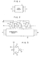
- the functional test of a logic circuit 1 shown in Fig. 1 is ordinarily performed in the manner as follows. First, test pattern signals are input from a plurality of input terminals 3 of the logic circuit. 1. Next, output signals which are output from a plurality of output terminals 5 are compared with expected values which have been preliminarily prepared. When the comparison results are coincident, it is determined that the logic circuit 1 operates accurately. In the case where the comparison-results are not coincident, it is determined that the logic circuit 1 is at fault.
- Fig. 2 shows one of logic circuits which may be used in the scan-path method.
- This circuit is a modification of the logic circuit shown in Fig. 7 of U.S. Patent 3,783,254.
- sequential circuit can be expressed as a combined form of registers 11-1 to 11-n and a combinational circuit 13.
- the sequential circuit of Fig. 2 further comprises changeover switches 15-1 to 15-n of the same structure.
- Fig. 3 shows one of these switches, e.g., the switch 15-1.
- a switch signal SW is supplied to the first input terminal of a 2-input AND gate 21.
- This signal SW is supplied via an inverter 23 to the first, input terminal of a 2-input AND gate 25.
- a scan input signal IN is supplied to the second input terminal of the AND gate 21.
- the second input terminal of the AND gate 25 is connected to the combinational circuit 13.
- the output terminals of the AND gates 21 and 25 are coupled to the first and second input terminals of a 2-input OR gate 27, the output terminal of which is coupled to the register 11-1.
- the registers 11-1 to 11-n store the data provided by the combinational circuit 13 as long as the switch signal SW is at the low level.
- the registers 11-1 to 11-n operate as a shift register when the switch signal SW is at the high level.
- the scan-path method is performed as follows. Test pattern signals are input from a plurality of input terminals 17 of the combinational circuit 13. Output signals from output terminals 19 are compared with expected values which have been preliminarily prepared. The switch signal SW is switched so that the registers 11-1 to 11-n constitute the shift registers. A pulse signal ⁇ for transference is input to the registers 11-1 to 11-n.
- the contents of the registers 11-1 to 11-n are shifted in response to the signal ⁇ .
- the contents of the registers 11-1 to 11-n are sequentially fetched as the output of the register 11-n.
- the contents of the respective registers 11-1 to 11-n, fetched as the output of the register 11-n are compared with the expected values which have been preliminarily prepared.
- the object of a functional test is to check whether a logic circuit works expectedly or not. It is ideal that a small number of input test patterns checks all the possible defects of logic components in a logic circuit.
- the number of input test patterns depends on how difficult the input signals control each logic node inside a logic circuit and make its logic state (high or low level) to propagate to output terminals. Increase of the number of-logic nodes and its complexity increase input test patterns. Increase of the number of output terminals, however, causes the decrease of input test patterns because defects of logic components can be detected more possibly at output terminals.
- registers play a role of additional output terminals. Since the logic circuit becomes more observable in ths scan-path method than the ordinary method, the number of test patterns of input signals which are input to the input terminals 17 can be reduced as compared with the ordinary method for the functional test described in conjunction with Fig. 1.
- the number of test patterns of input signals increases, as the constitution of the logic circuit 1 becomes complicated. It raises a problem such that it takes a long time to perform the full function test.
- the number of test patterns of input signals can be reduced by using registers as output terminals.
- observable points inside a logic circuit are limited on the inputs of the registers 11-1 to 11-n.
- the signal of each part of the combinational circuit 13 cannot be observed.
- a register has a larger number of elements which constitute the register function than an ordinary gate circuit or the like.
- this method has a drawback such that the scale of the whole circuit becomes large.
- an increase of the number of the registers 11-1 to 11-n causes the time needed to fetch the contents of these registers 11-1 to 11-n to the outside to increase. Therefore, there is a drawback such that it takes a long time to perform the functional test.
- This invention is made in consideration of the above-mentioned circumstances and the object of the invention is to provide a logic circuit which can easily and accurately perform its functional test in a short time.
- a logic circuit comprises: a logic section comprising a plurality of logic elements, for receiving at least one input signal, performing a predetermined logic operation and outputting at least one signal; and a detection circuit for receiving a control signal, receiving the output signals of the preselected logic elements of said logic elements and outputting a signal corresponding to the control signal and the output signals of the preselected logic elements, thereby detecting whether the preselected logic elements produce signals of values determined by the input signals of the logic section and by the control signal, and whether the logic section correctly operates.
- the logic circuit with such an arrangement, by comparing the output signals of the detection circuit with the expected values, it is possible to check whether the output signals of the preslected logic elements are correct or not.
- the functional test of the logic section is performed by respectively comparing the output signals of the logic section and the output signals of the detection circuit with the expected values. Therefore, it is possible to remarkably reduce the number of input test pattern signals to the logic section, thereby enabling the functional test of the logic section to be accurately performed in a short time.
- the-logic elements of which the failures are difficult to discover from the outside can be selected as the above-mentioned preselected logic elements. In such a case, it is possible to remarkably reduce the number of input test pattern signals to the logic section. Thus, it is possible to greatly shorten the time needed to perform the functional test.
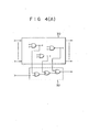
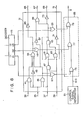
- a logic section 31 is constituted by various kinds of gates and registers, etc., and has a predetermined logic function. Further, it is provided with EX OR gates.
- the EX OR gates are connected in such a way that the output terminal of each of the EX OR gates is connected to one input terminal of the succeeding EX OR gates.
- the other input terminals of these EX OR gates are respectively connected to the output terminals of the preselected gates among the gates which constitute the logic section 31. (The preselected gates should be subjected to checking whether the output signals thereof are correct or not.)
- the logic section 31 has first to fourth input terminals 33, 35, 37 and 39.
- the first input terminal 33 is connected to a first input terminal of an AND gate 41.
- the second input terminal 35 is connected to a second input terminal of the AND gate 41, an inverter 43, and a first input terminal of an AND gate 45.
- the third input terminal 37 is connected to a second input terminal of the AND gate 45 and to a first input terminal of an NAND gate 47.
- the fourth input terminal 39 is connected to a second input terminal of the NAND gate 47, a second input terminal of the NAND gate 49, and an input terminal of an inverter 51.
- An output terminal of the AND gate 41, an output terminal of the inverter 43, and an output terminal of the AND gate 45 are connected to first, second and third input terminals of an OR gate 53, respectively.
- An output terminal of this OR gate 53 is connected to an input terminal of an inverter 55.
- the output terminal of the AND gate 45 is connected to an input terminal of an inverter 57.
- An output terminal of the inverter 57 is connected to a first input terminal of an OR gate 59.
- An output terminal of the NAND gate 47 is connected'to a first input terminal of the NAND gate 49 and a second. input terminal of an NAND gate 61.
- Output terminals of the NAND gates 61 and 49 are connected to-first and second input terminals of an NAND gate 63, respectively.
- An output terminal of the NAND gate 63 is connected to a second input terminal of the OR gate 59 and a first input terminal of the NAND gate 61.
- the inverter 55 is connected to a first output terminal 65 of the logic section 31.
- An output terminal of the OR gate 59 is connected to a second output terminal 67 of the logic section 31.
- the output terminal of the NAND gate 63 is connected through an inverter 73 to a third output terminal 69 of the logic section 31.
- An output terminal of the inverter 51 is connected to a fourth output terminal 71 of the logic section 31.
- a first input terminal of a first EX OR gate 75 is connected to the output terminal of the AND gate 45.
- An output terminal of the first EX OR gate 75 is connected to a second input terminal of a second EX OR gate 77.
- a first input terminal of the second EX OR gate 77 is connected to the output terminal of the OR gate 53.
- an output terminal of the second EX OR gate 77 is connected to a second input terminal of a third EX OR gate 79.
- a first input terminal of the third EX OR gate 79 is connected to the output terminal of the NAND gate 63.
- An output terminal of a control signal generator 81 is connected to a second input terminal of the first EX OR gate 75. This control signal generator 81 outputs a control signal SIG at a logic level "0" or "1".
- the functional test for the logic circuit with such an arrangement as described above is performed in the manner as follows.
- the function of a circuit hereafter referred to as an EX OR circuit 83 which is constituted by the first, second and third EX OR gates 75, 77 and 79 is tested.
- the logic level of the output signal SIG of the control signal generator 81 is inverted.
- the EX OR circuit 83 is not defective, the logic level of an output signal S of the third EX OR gate 79 is inverted. Therefore, when the control signal SIG is inverted, it is possible to discriminate whether the EX OR circuit 83 is at fault or not by checking if the signal S is inverted or not.
- control signal SIG When the control signal SIG is inverted, if the level of the signal S is inverted, it will be determined that the EX OR circuit 83 is not defective. On the other hand, when the control signal SIG is inverted, if the level of the signal S is not inverted, it will be determined that the EX OR circuit 83 shown in Fig. 4(B) is at fault.
- test pattern signals are then input to the input terminals 33, 35, 37 and 39 of the logic section 31.
- the signals are used by which the failure of the logic section 31 can be discovered.
- Those test pattern signals may be the same signals as the conventional ones.
- the output signals of the first to fourth output terminals 65, 67, 69 and 71 are compared with the expected values.
- the output signal S of the third EX OR gate 79 is compared with the expected value. By comparing the signal S with the expected value, it is possible to examine the output signals of the AND gate 45, OR gate 53 and NAND gate 63 to see if they are correct or not.
- the output signals of the logic section 31 are unconditionally determined.
- the output signals of the gates 45, 53 and 63 are also unconditionally determined.
- the output signal S of the third EX OR circuit 79 is also unconditionally determined.
- the control signal SIG been preset to either level of the logic levels "1" and "0".
- the output signal S becomes the logic level opposite to the expected value. Therefore, by checking the output signal S, the functional test for the logic section 31 can be also performed.
- the voltage of the output signal SIG of the control signal generator 81 is inverted, for example, from logic level "1" to "0".
- the EX OR circuit 83 is not defective.
- the test pattern signals are input to the first to fourth input terminals 33, 35, 37 and 39 of the logic section 31.
- the test pattern signals at the logic levels of "1", "1", "0", and "1" were input to the first to fourth input terminals 33, 35, 37 and 39, respectively.
- the control signal SIG is at the logic level of "1".
- the expected values of the output signals at the first to-fourth output terminals 65, 67, 69 and 71 are logic levels of "0", “1", “0” and “0", respectively.
- the output signals at the first to fourth output terminals 65, 67, 69 and 71 are compared with the above-mentioned expected values.
- the expected values of the output signals of the AND gate 45, OR gate 53 and NAND gate 63 are at logic levels of "0", "1” and “I", respectively. Therefore, the expected value of the output signal S is at logic level of "1".
- the actual output signals at the first to fourth output terminals 65, 67, 69 and 71 and the actual signal S are compared with the expected values.
- the AND gate 45 fails and the signal at logic level "1" is output.
- the output signals at the first to fourth output terminals 65, 67, 69 and 71 coincide with the expected values.
- the signal at level "1" is input to the first input terminal of the first EX OR gate 75.
- the signals at level "1” are respectively input to the first input terminals of the second and third EX OR gates 77 and 79.
- the output signal S becomes logic level "0", so that it is different from the expected value.
- the output signal S is inverted, so that it is detected that a defective portion exists in the logic section 31.
- the even number signals are ⁇ different from the normal levels, the signal S is not inverted, so that the presence of a failed portion in the logic section 31 cannot be detected.
- the number of input test pattern signals can be reduced.
- the EX OR circuit 83 is connected to the gates of which the failures are difficult to discover from the outside, the number of input test pattern signals can be remarkably reduced. Consequently, even when the logic circuit has high functions and a complicated circuit arrangement, the functional test thereof can be executed in a short time.
- the logic section 31 and EX OR circuit 83 may be formed on one semiconductor chip.
- Fig. 5 shows a modification of the logic circuit shown in Fig. 4(B).
- an inverter 85 has its input terminal connected to the output terminal of an AND gate 45, and its output terminal coupled to the first input terminal of a first EX OR gate 75.
- An inverter 87 has its input terminal coupled to the output terminal of an OR gate 53, and its output terminal connected to the first input terminal of a second EX OR gate 77.
- An inverter 89 has its input terminal connected to the output terminal of a NAND gate 63 and its output terminal coupled to the first input terminal of a third EX OR gate 79.
- the expected value of the output signal S of the third EX OR gate 79 is the inversion of the expected value of . the signal S generated by the circuit of Fig. 4(B).
- Fig. 6 is a circuit diagram showing an arrangement of a logic circuit according to another embodiment of the present invention.
- the parts and elements corresponding to those shown in Fig. 4(B) are designated by the same reference numerals and their descriptions will be omitted.
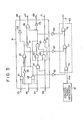
- a feature of the circuit shown in Fig. 6 is that first to third AND gates 95, 97 and 99 and a decoder 101 are provided.
- a first input terminal of a first AND gate 95 is connected to the output terminal of an AND gate 45.
- a second input terminal of the first AND gate 95 is connected to a first output terminal Ol of a decoder 101.
- an output terminal of. the first AND gate 95 is connected to the first input terminal of a first EX OR gate 75.
- a first input terminal of the second AND gate 97 is connected to the output terminal of an OR gate 53.
- a second input terminal of the second AND gate 97 is connected to a second output terminal 02 of the decoder 101.
- An output terminal of the second AND gate 97 is connected to the first input terminal of a second EX OR gate 77.
- a first input terminal of the third AND gate 99 is connected to the output terminal of a NAND gate 63.
- a second input terminal of the third AND gate 99 is connected to a third output terminal 03 of the decoder 101.
- the output terminal of the third AND gate 99 is connected to the first input terminal of a third EX OR gate 79.
- a selection signal of two bits is input to the input terminals Il, 12 of the decoder 101.
- a signal at logic level "1" is output from one of the three output terminals 01 to 03 in response to this 2-bit selection signal, while signals at logic level "0" are output from the other two output terminals.
- an EX OR circuit 83 is examined by use of a similar method as in the case of the circuit shown in Fig. 4(B).
- the test pattern signals are input to the first to fourth input terminals 33, 35, 37 and 39.
- the output signals from first to fourth output terminals 65, 67, 69 and 71 are compared with the expected values.
- the above-mentioned selection signal is input to the input terminals Il, I2 of the decoder 101, thereby a signal at logic level "1" is output from the first output terminal Ol.
- the output signal of the AND gate 45 is input through the first AND gate 95 to the first input terminal of the first EX OR gate 75.
- the second and third AND gates 97 and 99 output the signals at logic level "0".
- the signal S is compared with the expected value.
- the output signal of the AND gate 45 is determined to be correct.
- the output signal of the AND gate 45 is not correct, so that the logic section 31 is determined to be defective.
- the selection signal is switched and, for instance, the signal at logic level "1" is output from the second output terminal 02.
- the output signal of the OR gate 53 is input through the second AND gate 97 to the first input terminal of the second EX OR gate 77.
- the signal S is compared with the expected value.
- the selection signal is switched to examine whether the output signal of the NAND gate 63 is correct or not.
- the output signals of the AND gate 45, OR gate 53 and NAND gate 63 are checked to see if they are normal or not, respectively. Therefore, even if the even number signals (e.g., two) are simultaneously different from the correct levels, - it is possible to discriminate that the logic section 31 is at fault. Further, an approximate defective portion in the logic section 31 can be checked.
- OR gates may be merely used in place of the EX OR gates 75, 77 and 79.
- the use of OR gates enables the number of composing elements to be reduced as compared with that when the EX OR gates are used. Consequently, the invention is extremely effective when the number of signals needed to be checked in the logic section 31 is large.
- the output signals of the three gates 45, 53 and 63 were checked.
- the invention is not limited to this. Two, four, or more signals in the logic section 31 may be checked to see if they are correctly output or not.
- the number of signals checked may be an arbitrary number. Also, as the signals for examination, the signals of which the abnormality is difficult to discover from the outside (through the output signals of the logic section 31) are selected.
- the number of EX OR gates constituting the EX OR circuit 83 is also increased or decreased in association with the increase or decrease in the number of signals examined.
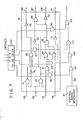
- Fig. 7 shows a logic circuit according to one embodiment of the present invention where OR gates are used in place of the first to third EX OR gates 75, 77 and 79 and where four signals are checked.
- a decoder 103 has three inputs and four outputs.
- a first input terminal of a fourth AND gate 105 is connected to the output terminal of an NAND gate 47.
- the second input terminals of first to fourth AND gates 95, 97, 99 and 105 are respectively connected to first, third, fourth, and second output terminals 01, 03, 04, and 02 of the decoder 103.
- the output terminals of the first to fourth AND gates 95, 97, 99 and 105 are connected to respective first input terminals of first, third, fourth, and second OR gates 107, lll, 113, and 109.
- the control signal generator 81 is connected to a second input terminal of the first OR gate 107.
- Output terminals of the first, second and third OR gates 107, 109 and 111 are connected to second input terminals of the second, third and fourth OR gates 109, 111 and 113, respectively. Even in the logic circuit shown in Fig. 7, a three-bit selection signal which is input to the decoder 103 is switched.
- the output signals of the AND gate 45, NAND gate 47, OR gate 53, and NAND gate 63 are sequentially checked to see if they are at the correct level or not by comparing the output signal of the fourth OR gate 113 with the expected value.
- the control signal SIG is set to logic level. "0".
- Fig. 8 shows a modification of the circuit shown in Fig. 6.
- the decoder 101 of the circuit of Fig. 6 is so designed as to output a signal of logic level "1" from one of the output terminals and signal of logic level "0" from the remaining two output . terminals. Which output terminal supplies a "1" level signal is determined by the selection signal supplied to the decoder 101.
- the circuit of Fig. 8 has a decoder 115 which is so designed as to output a signal of logic level "0" from one of the output terminals Ol to 03 and signals of logic level "1" from the remaining two output terminals. Which output terminal suplies a "0" level signal is determined by the selection signal supplied to the deocer 115.
- OR gates 117, l19 and 121 are used in place of the AND gates 95, 97 and 99 (Fig. 6).
- the signal from the terminal O1 is supplied to one input terminal of the a 2-input OR gate 117.
- the signal from the terminal 02 is supplied to one input terminal of a 2-input OR gate 119.
- the output signal from the terminal 03 is supplied to one input terminal of a 2-input OR gate 121.
- the expected value of the signal S produced by the circuit of Fig. 8 is the inversion of the expected value of the signal S output by the circuit of Fig. 6.
- Fig. 9 shows a modification of the circuit shown in Fig. 8.
- This circuit uses AND gates 123, 125, 127 instead of EX OR gates 75, 77 and 79 of the circuit shown in Fig. 8.
- the expected value of the AND gate 127 is equal to the expected value of the signal S produced by the circuit of Fig. 6.
- the EX OR gates 75, 77 and 79 may be replaced by one 4-input EX OR gate 129 as illustrated in Fig. 10. They may be replaced by any other logic gates or a circuit which performs the same exclusive OR operation.
- the OR gates 107, 109, 111 and 113 of the circuit shown in Fig. 7 may be replaced by one 5-input OR gate 131 as shown in Fig. 11. They may be replaced by any other gates or a circuit which performs the same OR operation.
- the AND gates 123, 125 and 127 of the circuit shown in Fig. 9 may be replaced by one 4-input AND gate 133 as shown in Fig. 12. They may be replaced by any other gates or a circuit which performs the same AND operation.
- the signals which are checked are not limited to the above-mentioned signals.
- This invention can be applied to logic circuits having a logic section with any arrangement.
- the examined signals are arbitrarily selected.
- the signals of which the abnormality is difficult to discover from the outside can be checked by this method.
- the number of signals examined can be an arbitrary number. Therefore, according to the present invention, even when the logic circuit has high functions and a complicated circuit arrangement, the number of input test pattern signals can be reduced and the functional test thereof can be accurately performed in a short time.
Abstract
Description
- The present invention relates to an improvement in a logic circuit and, more particularly, to a logic circuit which can easily perform its functional test.
- When installing an integrated circuit and the like, the functional test of the integrated circuit and the like are performed. For example, the functional test of a
logic circuit 1 shown in Fig. 1 is ordinarily performed in the manner as follows. First, test pattern signals are input from a plurality ofinput terminals 3 of the logic circuit. 1. Next, output signals which are output from a plurality ofoutput terminals 5 are compared with expected values which have been preliminarily prepared. When the comparison results are coincident, it is determined that thelogic circuit 1 operates accurately. In the case where the comparison-results are not coincident, it is determined that thelogic circuit 1 is at fault. - With respect to a sequential circuit among logic circuits, a method of a functional test, so-called scan-path method, is known. Fig. 2 shows one of logic circuits which may be used in the scan-path method. This circuit is a modification of the logic circuit shown in Fig. 7 of U.S. Patent 3,783,254. Generally, sequential circuit can be expressed as a combined form of registers 11-1 to 11-n and a
combinational circuit 13. The sequential circuit of Fig. 2 further comprises changeover switches 15-1 to 15-n of the same structure. Fig. 3 shows one of these switches, e.g., the switch 15-1. As shown in this figure, a switch signal SW is supplied to the first input terminal of a 2-input ANDgate 21. This signal SW is supplied via an inverter 23 to the first, input terminal of a 2-input ANDgate 25. A scan input signal IN is supplied to the second input terminal of theAND gate 21. The second input terminal of theAND gate 25 is connected to thecombinational circuit 13. The output terminals of theAND gates input OR gate 27, the output terminal of which is coupled to the register 11-1. - Since the other changeover switches 15-2 to 15-n have the same structure as the switch 15-1, the registers 11-1 to 11-n store the data provided by the
combinational circuit 13 as long as the switch signal SW is at the low level. On the other hand, the registers 11-1 to 11-n operate as a shift register when the switch signal SW is at the high level. The scan-path method is performed as follows. Test pattern signals are input from a plurality ofinput terminals 17 of thecombinational circuit 13. Output signals fromoutput terminals 19 are compared with expected values which have been preliminarily prepared. The switch signal SW is switched so that the registers 11-1 to 11-n constitute the shift registers. A pulse signal φ for transference is input to the registers 11-1 to 11-n. The contents of the registers 11-1 to 11-n are shifted in response to the signal ¢. The contents of the registers 11-1 to 11-n are sequentially fetched as the output of the register 11-n. The contents of the respective registers 11-1 to 11-n, fetched as the output of the register 11-n, are compared with the expected values which have been preliminarily prepared. The object of a functional test is to check whether a logic circuit works expectedly or not. It is ideal that a small number of input test patterns checks all the possible defects of logic components in a logic circuit. The number of input test patterns depends on how difficult the input signals control each logic node inside a logic circuit and make its logic state (high or low level) to propagate to output terminals. Increase of the number of-logic nodes and its complexity increase input test patterns. Increase of the number of output terminals, however, causes the decrease of input test patterns because defects of logic components can be detected more possibly at output terminals. - In the case of the scan-path method, registers play a role of additional output terminals. Since the logic circuit becomes more observable in ths scan-path method than the ordinary method, the number of test patterns of input signals which are input to the
input terminals 17 can be reduced as compared with the ordinary method for the functional test described in conjunction with Fig. 1. - According to the ordinary method for the functional test, the number of test patterns of input signals increases, as the constitution of the
logic circuit 1 becomes complicated. It raises a problem such that it takes a long time to perform the full function test. - On the other hand, according to the scan-path method, the number of test patterns of input signals can be reduced by using registers as output terminals. However, in this scan-path method, observable points inside a logic circuit are limited on the inputs of the registers 11-1 to 11-n. The signal of each part of the
combinational circuit 13 cannot be observed. In addition, when the increase of observable logic nodes is required, it is necessary to add registers to the logic circuit. A register has a larger number of elements which constitute the register function than an ordinary gate circuit or the like. Thus, this method has a drawback such that the scale of the whole circuit becomes large. Further, an increase of the number of the registers 11-1 to 11-n causes the time needed to fetch the contents of these registers 11-1 to 11-n to the outside to increase. Therefore, there is a drawback such that it takes a long time to perform the functional test. - With recent high integration and high density of semiconductor devices, the functional test is becoming more and more significant. With the high integration of semiconductor devices, however, there is a problem such that it takes a longer time to perform the functional test thereof.
- This invention is made in consideration of the above-mentioned circumstances and the object of the invention is to provide a logic circuit which can easily and accurately perform its functional test in a short time.
- A logic circuit according to this invention comprises: a logic section comprising a plurality of logic elements, for receiving at least one input signal, performing a predetermined logic operation and outputting at least one signal; and a detection circuit for receiving a control signal, receiving the output signals of the preselected logic elements of said logic elements and outputting a signal corresponding to the control signal and the output signals of the preselected logic elements, thereby detecting whether the preselected logic elements produce signals of values determined by the input signals of the logic section and by the control signal, and whether the logic section correctly operates.
- In the logic circuit with such an arrangement, by comparing the output signals of the detection circuit with the expected values, it is possible to check whether the output signals of the preslected logic elements are correct or not. The functional test of the logic section is performed by respectively comparing the output signals of the logic section and the output signals of the detection circuit with the expected values. Therefore, it is possible to remarkably reduce the number of input test pattern signals to the logic section, thereby enabling the functional test of the logic section to be accurately performed in a short time. In addition, the-logic elements of which the failures are difficult to discover from the outside can be selected as the above-mentioned preselected logic elements. In such a case, it is possible to remarkably reduce the number of input test pattern signals to the logic section. Thus, it is possible to greatly shorten the time needed to perform the functional test.
- This invention can be more fully understood from the following detailed description when taken in conjunction with the accompanying drawings, in which:
- Fig. 1 is a block diagram to explain an example of the functional test for a conventional logic circuit;
- Fig. 2 is a block diagram to explain an example of the conventional functional test of a sequential circuit;
- Fig. 3 is a circuit diagram of one of the changeover switches shown in Fig. 2;
- Fig. 4(A) is a circuit diagram showing the concept of the present invention;
- Fig. 4(B) is a circuit diagram showing an arrangement of a logic circuit according to one embodiment of the present invention; and
- Figs. 5 to 12 are circuit diagrams to explain arrangements of the logic circuits according to other embodiments of the present invention.
- Fig. 4(A) shows the idea of the present invention. As shown in this figure, three EX OR
gates 32 are cascade-connected. The input terminals of thesegates 32 are coupled to the output terminals of three preselected gates of alogic circuit 30 which comprises other gates of various types. - A logic circuit according to an embodiment of the invention will now be described with reference to Fig. 4(B).
- In Fig. 4(B), a
logic section 31 is constituted by various kinds of gates and registers, etc., and has a predetermined logic function. Further, it is provided with EX OR gates. The EX OR gates are connected in such a way that the output terminal of each of the EX OR gates is connected to one input terminal of the succeeding EX OR gates. The other input terminals of these EX OR gates are respectively connected to the output terminals of the preselected gates among the gates which constitute thelogic section 31. (The preselected gates should be subjected to checking whether the output signals thereof are correct or not.) The more complex thelogic section 31, the more effectively the present invention functions. For explanation, it is assumed that thelogic section 31 in this embodiment is constituted in the following manner. Thelogic section 31 has first tofourth input terminals first input terminal 33 is connected to a first input terminal of an ANDgate 41. Thesecond input terminal 35 is connected to a second input terminal of the ANDgate 41, aninverter 43, and a first input terminal of an ANDgate 45. Thethird input terminal 37 is connected to a second input terminal of the ANDgate 45 and to a first input terminal of anNAND gate 47. Thefourth input terminal 39 is connected to a second input terminal of theNAND gate 47, a second input terminal of theNAND gate 49, and an input terminal of aninverter 51. An output terminal of the ANDgate 41, an output terminal of theinverter 43, and an output terminal of the ANDgate 45 are connected to first, second and third input terminals of anOR gate 53, respectively. An output terminal of this ORgate 53 is connected to an input terminal of aninverter 55. The output terminal of the ANDgate 45 is connected to an input terminal of aninverter 57. An output terminal of theinverter 57 is connected to a first input terminal of anOR gate 59. An output terminal of theNAND gate 47 is connected'to a first input terminal of theNAND gate 49 and a second. input terminal of anNAND gate 61. Output terminals of theNAND gates NAND gate 63, respectively. An output terminal of theNAND gate 63 is connected to a second input terminal of theOR gate 59 and a first input terminal of theNAND gate 61. Theinverter 55 is connected to afirst output terminal 65 of thelogic section 31. An output terminal of theOR gate 59 is connected to asecond output terminal 67 of thelogic section 31. The output terminal of theNAND gate 63 is connected through aninverter 73 to athird output terminal 69 of thelogic section 31. An output terminal of theinverter 51 is connected to afourth output terminal 71 of thelogic section 31. In this embodiment, further a first input terminal of a firstEX OR gate 75 is connected to the output terminal of the ANDgate 45. An output terminal of the firstEX OR gate 75 is connected to a second input terminal of a secondEX OR gate 77. A first input terminal of the secondEX OR gate 77 is connected to the output terminal of theOR gate 53. Further, . an output terminal of the secondEX OR gate 77 is connected to a second input terminal of a thirdEX OR gate 79. A first input terminal of the thirdEX OR gate 79 is connected to the output terminal of theNAND gate 63. An output terminal of acontrol signal generator 81 is connected to a second input terminal of the firstEX OR gate 75. Thiscontrol signal generator 81 outputs a control signal SIG at a logic level "0" or "1". - Next, the functional test for the logic circuit with such an arrangement as described above is performed in the manner as follows. Prior to the functional test for the
logic section 31, the function of a circuit (hereafter referred to as an EX OR circuit 83) which is constituted by the first, second and third EX ORgates control signal generator 81 is inverted. When theEX OR circuit 83 is not defective, the logic level of an output signal S of the thirdEX OR gate 79 is inverted. Therefore, when the control signal SIG is inverted, it is possible to discriminate whether theEX OR circuit 83 is at fault or not by checking if the signal S is inverted or not. When the control signal SIG is inverted, if the level of the signal S is inverted, it will be determined that theEX OR circuit 83 is not defective. On the other hand, when the control signal SIG is inverted, if the level of the signal S is not inverted, it will be determined that theEX OR circuit 83 shown in Fig. 4(B) is at fault. - When the
EX OR circuit 83 has determined from the above test that it is not at fault, predetermined test pattern signals are then input to theinput terminals logic section 31. On the other hand, with these test pattern signals, the signals are used by which the failure of thelogic section 31 can be discovered. Those test pattern signals may be the same signals as the conventional ones. The output signals of the first tofourth output terminals EX OR gate 79 is compared with the expected value. By comparing the signal S with the expected value, it is possible to examine the output signals of the ANDgate 45, ORgate 53 andNAND gate 63 to see if they are correct or not. Namely, when the constant test pattern signals are input to thelogic section 31, the output signals of thelogic section 31 are unconditionally determined. In addition, the output signals of thegates EX OR circuit 79 is also unconditionally determined. In this. case, the control signal SIG been preset to either level of the logic levels "1" and "0". In the case where one of the output signals of thegates logic section 31 can be also performed. When the output signal S coincides with the expected value and the output signals from the first to fourth output terminals coincide with the expected values, it is determined that thislogic section 31 is not at fault. In a similar manner as above, the next test pattern signals are input. Thereafter, the functional test is again conducted on thelogic section 31. - When all the output signals of the
logic section 31 and the signals S are found equal to the expected values after all the test pattern signals have been input, it is determined at least that thelogic section 31 is not faulty. - The method of performing the functional test for the circuit shown in Fig. 4(B) will now be explained below by use of a practical example. First, the voltage of the output signal SIG of the
control signal generator 81 is inverted, for example, from logic level "1" to "0". When the signal S is inverted, theEX OR circuit 83 is not defective. The test pattern signals are input to the first tofourth input terminals logic section 31. For explanation, it is assumed that the test pattern signals at the logic levels of "1", "1", "0", and "1" were input to the first tofourth input terminals fourth output terminals fourth output terminals gate 45, ORgate 53 andNAND gate 63 are at logic levels of "0", "1" and "I", respectively. Therefore, the expected value of the output signal S is at logic level of "1". The actual output signals at the first tofourth output terminals gate 45 fails and the signal at logic level "1" is output. At this time the output signals at the first tofourth output terminals fourth output terminals logic section 31 is at fault. On the other hand, the signal at level "1" is input to the first input terminal of the firstEX OR gate 75. While, the signals at level "1" are respectively input to the first input terminals of the second and third EX ORgates logic section 31 is defective. - In the foregoing embodiment, when the odd number signals are different from the normal (expected) levels, the output signal S is inverted, so that it is detected that a defective portion exists in the
logic section 31. On the other hand, when the even number signals are·different from the normal levels, the signal S is not inverted, so that the presence of a failed portion in thelogic section 31 cannot be detected. - When performing the functional test for the
logic section 31, as the number of signals which can be observed on the outside is larger, the number of input test pattern signals can be reduced. In the above embodiment, in addition to the output signals from the first tofourth output terminals logic section 31 are correct or not. Thus, this enables the number of input test pattern signals to be reduced compared to the conventional ones. Particularly, if theEX OR circuit 83 is connected to the gates of which the failures are difficult to discover from the outside, the number of input test pattern signals can be remarkably reduced. Consequently, even when the logic circuit has high functions and a complicated circuit arrangement, the functional test thereof can be executed in a short time. On the other hand, when compared with the conventional scan-path method, in the logic circuit according to the foregoing embodiment, it is possible to select only the necessary number of output signals of the arbitrary gates and to examine them. Also, these signals can be checked through theEX OR circuit 83 in a short time. Therefore, it is possible to realize the remarkable reduction of the time period to perform the functional test even when compared to the above-mentioned scan-path method. - The
logic section 31 andEX OR circuit 83 may be formed on one semiconductor chip. - Fig. 5 shows a modification of the logic circuit shown in Fig. 4(B). As shown in Fig. 5, an
inverter 85 has its input terminal connected to the output terminal of an ANDgate 45, and its output terminal coupled to the first input terminal of a firstEX OR gate 75. Aninverter 87 has its input terminal coupled to the output terminal of anOR gate 53, and its output terminal connected to the first input terminal of a secondEX OR gate 77. Aninverter 89 has its input terminal connected to the output terminal of aNAND gate 63 and its output terminal coupled to the first input terminal of a thirdEX OR gate 79. The expected value of the output signal S of the thirdEX OR gate 79 is the inversion of the expected value of . the signal S generated by the circuit of Fig. 4(B). - Fig. 6 is a circuit diagram showing an arrangement of a logic circuit according to another embodiment of the present invention. In addition, in Fig. 6, the parts and elements corresponding to those shown in Fig. 4(B) are designated by the same reference numerals and their descriptions will be omitted. A feature of the circuit shown in Fig. 6 is that first to third AND
gates decoder 101 are provided. In Fig. 6, a first input terminal of a first ANDgate 95 is connected to the output terminal of an ANDgate 45. A second input terminal of the first ANDgate 95 is connected to a first output terminal Ol of adecoder 101. Further, an output terminal of. the first ANDgate 95 is connected to the first input terminal of a firstEX OR gate 75. A first input terminal of the second ANDgate 97 is connected to the output terminal of anOR gate 53. A second input terminal of the second ANDgate 97 is connected to asecond output terminal 02 of thedecoder 101. An output terminal of the second ANDgate 97 is connected to the first input terminal of a secondEX OR gate 77. A first input terminal of the third ANDgate 99 is connected to the output terminal of aNAND gate 63. A second input terminal of the third ANDgate 99 is connected to athird output terminal 03 of thedecoder 101. The output terminal of the third ANDgate 99 is connected to the first input terminal of a thirdEX OR gate 79. For example, a selection signal of two bits is input to the input terminals Il, 12 of thedecoder 101. A signal at logic level "1" is output from one of the threeoutput terminals 01 to 03 in response to this 2-bit selection signal, while signals at logic level "0" are output from the other two output terminals. - A method of performing the functional test for the logic circuit shown in Fig. 6 will now be explained.
- The operation of an
EX OR circuit 83 is examined by use of a similar method as in the case of the circuit shown in Fig. 4(B). Next, the test pattern signals are input to the first tofourth input terminals fourth output terminals decoder 101, thereby a signal at logic level "1" is output from the first output terminal Ol. This makes the first ANDgate 95 open. The output signal of the ANDgate 45 is input through the first ANDgate 95 to the first input terminal of the firstEX OR gate 75. At this time, the second and third ANDgates gate 45 is determined to be correct. On the other hand, when the signal S is different from the expected value, the output signal of the ANDgate 45 is not correct, so that thelogic section 31 is determined to be defective. Next, the selection signal is switched and, for instance, the signal at logic level "1" is output from thesecond output terminal 02. The output signal of theOR gate 53 is input through the second ANDgate 97 to the first input terminal of the secondEX OR gate 77. The signal S is compared with the expected value. Similarly, the selection signal is switched to examine whether the output signal of theNAND gate 63 is correct or not. In the circuit shown in Fig. 6, the output signals of the ANDgate 45, ORgate 53 andNAND gate 63 are checked to see if they are normal or not, respectively. Therefore, even if the even number signals (e.g., two) are simultaneously different from the correct levels, - it is possible to discriminate that thelogic section 31 is at fault. Further, an approximate defective portion in thelogic section 31 can be checked. - In case of this embodiment, it is necessary to check the output signals of the
gates decoder 101. Therefore, it takes a slightly longer time for the functional test than that of Fig. 4(B); however, the invention is extremely effective for a logic circuit having a large probability of failure occurrence. - In the foregoing embodiment, the output signals of the
gates decoder 101; therefore, OR gates may be merely used in place of the EX ORgates logic section 31 is large. In addition, in the embodiments shown in Figs. 4(B), 5 and 6, the output signals of the threegates logic section 31 may be checked to see if they are correctly output or not. The number of signals checked may be an arbitrary number. Also, as the signals for examination, the signals of which the abnormality is difficult to discover from the outside (through the output signals of the logic section 31) are selected. The number of EX OR gates constituting theEX OR circuit 83 is also increased or decreased in association with the increase or decrease in the number of signals examined. - Fig. 7 shows a logic circuit according to one embodiment of the present invention where OR gates are used in place of the first to third EX OR
gates gate 105 is connected to the output terminal of anNAND gate 47. The second input terminals of first to fourth ANDgates second output terminals gates gates 107, lll, 113, and 109. Thecontrol signal generator 81 is connected to a second input terminal of the first ORgate 107. Output terminals of the first, second and third ORgates gates gate 45,NAND gate 47, ORgate 53, andNAND gate 63 are sequentially checked to see if they are at the correct level or not by comparing the output signal of the fourth ORgate 113 with the expected value. When using the first to fourth ORgates - Fig. 8 shows a modification of the circuit shown in Fig. 6. The
decoder 101 of the circuit of Fig. 6 is so designed as to output a signal of logic level "1" from one of the output terminals and signal of logic level "0" from the remaining two output . terminals. Which output terminal supplies a "1" level signal is determined by the selection signal supplied to thedecoder 101. On the other hand, the circuit of Fig. 8 has adecoder 115 which is so designed as to output a signal of logic level "0" from one of the output terminals Ol to 03 and signals of logic level "1" from the remaining two output terminals. Which output terminal suplies a "0" level signal is determined by the selection signal supplied to thedeocer 115. In this circuit, ORgates 117, l19 and 121 are used in place of the ANDgates gate 117. The signal from the terminal 02 is supplied to one input terminal of a 2-input ORgate 119. The output signal from the terminal 03 is supplied to one input terminal of a 2-input ORgate 121. The expected value of the signal S produced by the circuit of Fig. 8 is the inversion of the expected value of the signal S output by the circuit of Fig. 6. - Fig. 9 shows a modification of the circuit shown in Fig. 8. This circuit uses AND
gates gates gate 127 is equal to the expected value of the signal S produced by the circuit of Fig. 6. - Of course, in the circuits of Figs. 4(B), 5, 6' and 8, the EX OR
gates EX OR gate 129 as illustrated in Fig. 10. They may be replaced by any other logic gates or a circuit which performs the same exclusive OR operation. Further, the ORgates gate 131 as shown in Fig. 11. They may be replaced by any other gates or a circuit which performs the same OR operation. Furthermore, the ANDgates gate 133 as shown in Fig. 12. They may be replaced by any other gates or a circuit which performs the same AND operation. - In the logic circuits shown in Figs. 4(B) - 9, one example has been shown for explaining as the arrangement of each
logic section 31; the invention is not limited to this. In addition, the signals which are checked are not limited to the above-mentioned signals. This invention can be applied to logic circuits having a logic section with any arrangement. The examined signals are arbitrarily selected. In particular, the signals of which the abnormality is difficult to discover from the outside can be checked by this method. Further, the number of signals examined can be an arbitrary number. Therefore, according to the present invention, even when the logic circuit has high functions and a complicated circuit arrangement, the number of input test pattern signals can be reduced and the functional test thereof can be accurately performed in a short time.
Claims (11)
Applications Claiming Priority (2)
| Application Number | Priority Date | Filing Date | Title |
|---|---|---|---|
| JP196767/83 | 1983-10-20 | ||
| JP58196767A JPS6088370A (en) | 1983-10-20 | 1983-10-20 | Logical circuit |
Publications (3)
| Publication Number | Publication Date |
|---|---|
| EP0151694A2 true EP0151694A2 (en) | 1985-08-21 |
| EP0151694A3 EP0151694A3 (en) | 1988-04-20 |
| EP0151694B1 EP0151694B1 (en) | 1993-02-03 |
Family
ID=16363279
Family Applications (1)
| Application Number | Title | Priority Date | Filing Date |
|---|---|---|---|
| EP84112567A Expired - Lifetime EP0151694B1 (en) | 1983-10-20 | 1984-10-18 | Logic circuit with built-in self-test function |
Country Status (4)
| Country | Link |
|---|---|
| US (1) | US4682331A (en) |
| EP (1) | EP0151694B1 (en) |
| JP (1) | JPS6088370A (en) |
| DE (1) | DE3486064T2 (en) |
Cited By (4)
| Publication number | Priority date | Publication date | Assignee | Title |
|---|---|---|---|---|
| EP0223714A2 (en) * | 1985-11-20 | 1987-05-27 | Fujitsu Limited | Semiconductor integrated circuit device with test circuit |
| EP0286920A2 (en) * | 1987-04-13 | 1988-10-19 | Prime Computer, Inc. | Method and apparatus for high accuracy measurement of VLSI components |
| EP0307503A1 (en) * | 1986-03-10 | 1989-03-22 | Cross-Check Technology, Inc. | A grid-based, "cross-check" test structure for testing integrated circuits |
| US5065090A (en) * | 1988-07-13 | 1991-11-12 | Cross-Check Technology, Inc. | Method for testing integrated circuits having a grid-based, "cross-check" te |
Families Citing this family (4)
| Publication number | Priority date | Publication date | Assignee | Title |
|---|---|---|---|---|
| JPH03211481A (en) * | 1990-01-17 | 1991-09-17 | Nec Corp | Lsi test circuit |
| JPH06295599A (en) * | 1993-04-09 | 1994-10-21 | Nec Corp | Semiconductor memory device |
| US5960009A (en) * | 1996-08-09 | 1999-09-28 | Lucent Technologies Inc. | Built in shelf test method and apparatus for booth multipliers |
| US20050050422A1 (en) * | 2003-08-27 | 2005-03-03 | Noriko Jo | Semiconductor integrated circuit |
Family Cites Families (10)
| Publication number | Priority date | Publication date | Assignee | Title |
|---|---|---|---|---|
| US3559167A (en) * | 1968-07-25 | 1971-01-26 | Ibm | Self-checking error checker for two-rail coded data |
| US3783254A (en) * | 1972-10-16 | 1974-01-01 | Ibm | Level sensitive logic system |
| US4001818A (en) * | 1975-10-22 | 1977-01-04 | Storage Technology Corporation | Digital circuit failure detector |
| US4176258A (en) * | 1978-05-01 | 1979-11-27 | Intel Corporation | Method and circuit for checking integrated circuit chips |
| US4242751A (en) * | 1978-08-28 | 1980-12-30 | Genrad, Inc. | Automatic fault-probing method and apparatus for checking electrical circuits and the like |
| US4271515A (en) * | 1979-03-23 | 1981-06-02 | John Fluke Mfg. Co., Inc. | Universal analog and digital tester |
| US4328583A (en) * | 1980-09-08 | 1982-05-04 | Rockwell International Corporation | Data bus fault detector |
| US4412327A (en) * | 1981-02-25 | 1983-10-25 | Western Electric Company, Inc. | Test circuit for checking memory output state continuously during time window |
| US4541090A (en) * | 1981-06-09 | 1985-09-10 | Matsushita Electric Industrial Co., Ltd. | Semiconductor memory device |
| US4498172A (en) * | 1982-07-26 | 1985-02-05 | General Electric Company | System for polynomial division self-testing of digital networks |
-
1983
- 1983-10-20 JP JP58196767A patent/JPS6088370A/en active Pending
-
1984
- 1984-10-18 DE DE8484112567T patent/DE3486064T2/en not_active Expired - Fee Related
- 1984-10-18 EP EP84112567A patent/EP0151694B1/en not_active Expired - Lifetime
- 1984-10-18 US US06/662,142 patent/US4682331A/en not_active Expired - Lifetime
Non-Patent Citations (3)
| Title |
|---|
| IBM JOURNAL OF RESEARCH AND DEVELOPMENT, vol. 27, no. 3, May 1983, pages 265-272, New York, US; E.B. EICHELBERGER et al.: "Random-pattern coverage enhancement and diagnosis for LSSD logic self-test" * |
| IBM TECHNICAL DISCLOSURE BULLETIN, vol. 14, no. 10, March 1972, pages 2937,2938, New York, US; A.D. SAVKAR: "N-way testpoint for complex LSI design" * |
| SYSTEMS.COMPUTERS.CONTROLS, vol. 7, no. 2, March/April 1976, pages 19-25, Washington, D.C., US; M. YAMAMOTO: "Modification of Reddy's easily testable network and its application to sequential circuits" * |
Cited By (6)
| Publication number | Priority date | Publication date | Assignee | Title |
|---|---|---|---|---|
| EP0223714A2 (en) * | 1985-11-20 | 1987-05-27 | Fujitsu Limited | Semiconductor integrated circuit device with test circuit |
| EP0223714A3 (en) * | 1985-11-20 | 1988-09-14 | Fujitsu Limited | Semiconductor integrated circuit device with test circuit |
| EP0307503A1 (en) * | 1986-03-10 | 1989-03-22 | Cross-Check Technology, Inc. | A grid-based, "cross-check" test structure for testing integrated circuits |
| EP0286920A2 (en) * | 1987-04-13 | 1988-10-19 | Prime Computer, Inc. | Method and apparatus for high accuracy measurement of VLSI components |
| EP0286920A3 (en) * | 1987-04-13 | 1991-03-06 | Prime Computer, Inc. | Method and apparatus for high accuracy measurement of vlsi components |
| US5065090A (en) * | 1988-07-13 | 1991-11-12 | Cross-Check Technology, Inc. | Method for testing integrated circuits having a grid-based, "cross-check" te |
Also Published As
| Publication number | Publication date |
|---|---|
| JPS6088370A (en) | 1985-05-18 |
| DE3486064D1 (en) | 1993-03-18 |
| EP0151694B1 (en) | 1993-02-03 |
| US4682331A (en) | 1987-07-21 |
| EP0151694A3 (en) | 1988-04-20 |
| DE3486064T2 (en) | 1993-07-15 |
Similar Documents
| Publication | Publication Date | Title |
|---|---|---|
| US6861866B2 (en) | System on chip (SOC) and method of testing and/or debugging the system on chip | |
| EP0023972B1 (en) | A system of functional units for performing logic functions | |
| US5588006A (en) | Logic circuit having a control signal switching logic function and having a testing arrangement | |
| US6877119B2 (en) | Circuit scan output arrangement | |
| US6708301B1 (en) | Functional block for integrated circuit, semiconductor integrated circuit, inspection method for semiconductor integrated circuit, and designing method therefor | |
| EP0151694A2 (en) | Logic circuit with built-in self-test function | |
| US7752514B2 (en) | Methods and apparatus for testing a scan chain to isolate defects | |
| KR19980032360A (en) | Scan test method of semiconductor integrated circuit | |
| US7895489B2 (en) | Matrix system and method for debugging scan structure | |
| US5425035A (en) | Enhanced data analyzer for use in bist circuitry | |
| US7284171B2 (en) | Integrated circuit device | |
| US5513189A (en) | Boundary scan system with improved error reporting using sentinel bit patterns | |
| US20030226079A1 (en) | Scan-path flip-flop circuit for integrated circuit memory | |
| JP4176716B2 (en) | Electronic circuit with test unit | |
| JP2937811B2 (en) | Semiconductor integrated circuit test circuit and test method thereof | |
| US6321355B1 (en) | Semiconductor integrated circuit and method of testing the same | |
| US6553528B1 (en) | Test circuit for semiconductor integrated circuit | |
| US6421810B1 (en) | Scalable parallel test bus and testing method | |
| CN117420412A (en) | Integrated circuit scanning test system and equipment | |
| JPH10124564A (en) | Inspection-facilitated designing method, bus error-evaded designing method and integrated circuit | |
| JPS6173075A (en) | Extraction system for lsi logical state | |
| JPH0666885A (en) | Boundary scanning circuit | |
| JPS6088371A (en) | Logical circuit | |
| JP2001229696A (en) | Semiconductor integrated circuit and its test method | |
| JPS6318597A (en) | Memory test device for incorporated circuit |
Legal Events
| Date | Code | Title | Description |
|---|---|---|---|
| PUAI | Public reference made under article 153(3) epc to a published international application that has entered the european phase |
Free format text: ORIGINAL CODE: 0009012 |
|
| 17P | Request for examination filed |
Effective date: 19841018 |
|
| AK | Designated contracting states |
Designated state(s): DE FR GB |
|
| PUAL | Search report despatched |
Free format text: ORIGINAL CODE: 0009013 |
|
| AK | Designated contracting states |
Kind code of ref document: A3 Designated state(s): DE FR GB |
|
| 17Q | First examination report despatched |
Effective date: 19891102 |
|
| GRAA | (expected) grant |
Free format text: ORIGINAL CODE: 0009210 |
|
| AK | Designated contracting states |
Kind code of ref document: B1 Designated state(s): DE FR GB |
|
| REF | Corresponds to: |
Ref document number: 3486064 Country of ref document: DE Date of ref document: 19930318 |
|
| ET | Fr: translation filed | ||
| PLBE | No opposition filed within time limit |
Free format text: ORIGINAL CODE: 0009261 |
|
| STAA | Information on the status of an ep patent application or granted ep patent |
Free format text: STATUS: NO OPPOSITION FILED WITHIN TIME LIMIT |
|
| 26N | No opposition filed | ||
| PGFP | Annual fee paid to national office [announced via postgrant information from national office to epo] |
Ref country code: GB Payment date: 19971009 Year of fee payment: 14 Ref country code: FR Payment date: 19971009 Year of fee payment: 14 |
|
| PGFP | Annual fee paid to national office [announced via postgrant information from national office to epo] |
Ref country code: DE Payment date: 19971024 Year of fee payment: 14 |
|
| PG25 | Lapsed in a contracting state [announced via postgrant information from national office to epo] |
Ref country code: GB Free format text: LAPSE BECAUSE OF NON-PAYMENT OF DUE FEES Effective date: 19981018 |
|
| GBPC | Gb: european patent ceased through non-payment of renewal fee |
Effective date: 19981018 |
|
| PG25 | Lapsed in a contracting state [announced via postgrant information from national office to epo] |
Ref country code: FR Free format text: LAPSE BECAUSE OF NON-PAYMENT OF DUE FEES Effective date: 19990630 |
|
| REG | Reference to a national code |
Ref country code: FR Ref legal event code: ST |
|
| PG25 | Lapsed in a contracting state [announced via postgrant information from national office to epo] |
Ref country code: DE Free format text: LAPSE BECAUSE OF NON-PAYMENT OF DUE FEES Effective date: 19990803 |