EP0148031B1 - Semiconductor device - Google Patents
Semiconductor device Download PDFInfo
- Publication number
- EP0148031B1 EP0148031B1 EP84309131A EP84309131A EP0148031B1 EP 0148031 B1 EP0148031 B1 EP 0148031B1 EP 84309131 A EP84309131 A EP 84309131A EP 84309131 A EP84309131 A EP 84309131A EP 0148031 B1 EP0148031 B1 EP 0148031B1
- Authority
- EP
- European Patent Office
- Prior art keywords
- semiconductor layer
- type
- layer
- semiconductor
- transistor
- Prior art date
- Legal status (The legal status is an assumption and is not a legal conclusion. Google has not performed a legal analysis and makes no representation as to the accuracy of the status listed.)
- Expired
Links
- 239000004065 semiconductor Substances 0.000 title claims description 80
- 239000000969 carrier Substances 0.000 claims description 33
- 239000000758 substrate Substances 0.000 claims description 23
- 239000012535 impurity Substances 0.000 claims description 16
- JBRZTFJDHDCESZ-UHFFFAOYSA-N AsGa Chemical compound [As]#[Ga] JBRZTFJDHDCESZ-UHFFFAOYSA-N 0.000 description 36
- VYPSYNLAJGMNEJ-UHFFFAOYSA-N Silicium dioxide Chemical compound O=[Si]=O VYPSYNLAJGMNEJ-UHFFFAOYSA-N 0.000 description 24
- 238000000034 method Methods 0.000 description 16
- 238000010586 diagram Methods 0.000 description 14
- 229910052681 coesite Inorganic materials 0.000 description 12
- 229910052906 cristobalite Inorganic materials 0.000 description 12
- 239000000377 silicon dioxide Substances 0.000 description 12
- 235000012239 silicon dioxide Nutrition 0.000 description 12
- 229910052682 stishovite Inorganic materials 0.000 description 12
- 229910052905 tridymite Inorganic materials 0.000 description 12
- 238000009792 diffusion process Methods 0.000 description 11
- 239000011701 zinc Substances 0.000 description 9
- 238000005468 ion implantation Methods 0.000 description 8
- 125000004429 atom Chemical group 0.000 description 6
- 238000001451 molecular beam epitaxy Methods 0.000 description 6
- 230000001133 acceleration Effects 0.000 description 5
- 239000000370 acceptor Substances 0.000 description 5
- 238000003486 chemical etching Methods 0.000 description 5
- 230000005669 field effect Effects 0.000 description 5
- 150000002500 ions Chemical class 0.000 description 5
- 238000002955 isolation Methods 0.000 description 5
- 229910052751 metal Inorganic materials 0.000 description 5
- 239000002184 metal Substances 0.000 description 5
- 229920002120 photoresistant polymer Polymers 0.000 description 5
- 230000005533 two-dimensional electron gas Effects 0.000 description 5
- 238000000137 annealing Methods 0.000 description 4
- 239000002019 doping agent Substances 0.000 description 4
- 230000000694 effects Effects 0.000 description 4
- 238000005530 etching Methods 0.000 description 4
- 239000007789 gas Substances 0.000 description 4
- 238000002513 implantation Methods 0.000 description 4
- 230000010354 integration Effects 0.000 description 4
- 239000003708 ampul Substances 0.000 description 3
- 239000000463 material Substances 0.000 description 3
- RBFQJDQYXXHULB-UHFFFAOYSA-N arsane Chemical compound [AsH3] RBFQJDQYXXHULB-UHFFFAOYSA-N 0.000 description 2
- 229910000070 arsenic hydride Inorganic materials 0.000 description 2
- 229910001423 beryllium ion Inorganic materials 0.000 description 2
- 150000001875 compounds Chemical class 0.000 description 2
- 239000013078 crystal Substances 0.000 description 2
- AXAZMDOAUQTMOW-UHFFFAOYSA-N dimethylzinc Chemical compound C[Zn]C AXAZMDOAUQTMOW-UHFFFAOYSA-N 0.000 description 2
- 239000003574 free electron Substances 0.000 description 2
- XCZXGTMEAKBVPV-UHFFFAOYSA-N trimethylgallium Chemical compound C[Ga](C)C XCZXGTMEAKBVPV-UHFFFAOYSA-N 0.000 description 2
- 229910000980 Aluminium gallium arsenide Inorganic materials 0.000 description 1
- 108091006149 Electron carriers Proteins 0.000 description 1
- 229910000530 Gallium indium arsenide Inorganic materials 0.000 description 1
- 229910000673 Indium arsenide Inorganic materials 0.000 description 1
- 235000010627 Phaseolus vulgaris Nutrition 0.000 description 1
- 244000046052 Phaseolus vulgaris Species 0.000 description 1
- BLRPTPMANUNPDV-UHFFFAOYSA-N Silane Chemical compound [SiH4] BLRPTPMANUNPDV-UHFFFAOYSA-N 0.000 description 1
- 238000005275 alloying Methods 0.000 description 1
- 229910052785 arsenic Inorganic materials 0.000 description 1
- 230000008033 biological extinction Effects 0.000 description 1
- 230000015556 catabolic process Effects 0.000 description 1
- 238000010276 construction Methods 0.000 description 1
- PXBRQCKWGAHEHS-UHFFFAOYSA-N dichlorodifluoromethane Chemical compound FC(F)(Cl)Cl PXBRQCKWGAHEHS-UHFFFAOYSA-N 0.000 description 1
- 235000019404 dichlorodifluoromethane Nutrition 0.000 description 1
- 230000005684 electric field Effects 0.000 description 1
- 238000001704 evaporation Methods 0.000 description 1
- 230000008020 evaporation Effects 0.000 description 1
- 239000004047 hole gas Substances 0.000 description 1
- 230000006698 induction Effects 0.000 description 1
- 239000012212 insulator Substances 0.000 description 1
- 238000004519 manufacturing process Methods 0.000 description 1
- 230000007246 mechanism Effects 0.000 description 1
- 150000002739 metals Chemical class 0.000 description 1
- 239000000203 mixture Substances 0.000 description 1
- 125000004430 oxygen atom Chemical group O* 0.000 description 1
- 238000005268 plasma chemical vapour deposition Methods 0.000 description 1
- 238000005036 potential barrier Methods 0.000 description 1
- 238000003672 processing method Methods 0.000 description 1
- 230000001105 regulatory effect Effects 0.000 description 1
- 229910021332 silicide Inorganic materials 0.000 description 1
- FVBUAEGBCNSCDD-UHFFFAOYSA-N silicide(4-) Chemical compound [Si-4] FVBUAEGBCNSCDD-UHFFFAOYSA-N 0.000 description 1
- 125000006850 spacer group Chemical group 0.000 description 1
- 241000894007 species Species 0.000 description 1
- JLTRXTDYQLMHGR-UHFFFAOYSA-N trimethylaluminium Chemical compound C[Al](C)C JLTRXTDYQLMHGR-UHFFFAOYSA-N 0.000 description 1
- 230000005641 tunneling Effects 0.000 description 1
- 229910052725 zinc Inorganic materials 0.000 description 1
Images


Classifications
-
- H—ELECTRICITY
- H01—ELECTRIC ELEMENTS
- H01L—SEMICONDUCTOR DEVICES NOT COVERED BY CLASS H10
- H01L29/00—Semiconductor devices adapted for rectifying, amplifying, oscillating or switching, or capacitors or resistors with at least one potential-jump barrier or surface barrier, e.g. PN junction depletion layer or carrier concentration layer; Details of semiconductor bodies or of electrodes thereof ; Multistep manufacturing processes therefor
- H01L29/66—Types of semiconductor device ; Multistep manufacturing processes therefor
- H01L29/68—Types of semiconductor device ; Multistep manufacturing processes therefor controllable by only the electric current supplied, or only the electric potential applied, to an electrode which does not carry the current to be rectified, amplified or switched
- H01L29/70—Bipolar devices
- H01L29/74—Thyristor-type devices, e.g. having four-zone regenerative action
-
- H—ELECTRICITY
- H01—ELECTRIC ELEMENTS
- H01L—SEMICONDUCTOR DEVICES NOT COVERED BY CLASS H10
- H01L29/00—Semiconductor devices adapted for rectifying, amplifying, oscillating or switching, or capacitors or resistors with at least one potential-jump barrier or surface barrier, e.g. PN junction depletion layer or carrier concentration layer; Details of semiconductor bodies or of electrodes thereof ; Multistep manufacturing processes therefor
- H01L29/66—Types of semiconductor device ; Multistep manufacturing processes therefor
- H01L29/68—Types of semiconductor device ; Multistep manufacturing processes therefor controllable by only the electric current supplied, or only the electric potential applied, to an electrode which does not carry the current to be rectified, amplified or switched
- H01L29/76—Unipolar devices, e.g. field effect transistors
- H01L29/772—Field effect transistors
- H01L29/778—Field effect transistors with two-dimensional charge carrier gas channel, e.g. HEMT ; with two-dimensional charge-carrier layer formed at a heterojunction interface
- H01L29/7786—Field effect transistors with two-dimensional charge carrier gas channel, e.g. HEMT ; with two-dimensional charge-carrier layer formed at a heterojunction interface with direct single heterostructure, i.e. with wide bandgap layer formed on top of active layer, e.g. direct single heterostructure MIS-like HEMT
- H01L29/7787—Field effect transistors with two-dimensional charge carrier gas channel, e.g. HEMT ; with two-dimensional charge-carrier layer formed at a heterojunction interface with direct single heterostructure, i.e. with wide bandgap layer formed on top of active layer, e.g. direct single heterostructure MIS-like HEMT with wide bandgap charge-carrier supplying layer, e.g. direct single heterostructure MODFET
-
- H—ELECTRICITY
- H01—ELECTRIC ELEMENTS
- H01L—SEMICONDUCTOR DEVICES NOT COVERED BY CLASS H10
- H01L29/00—Semiconductor devices adapted for rectifying, amplifying, oscillating or switching, or capacitors or resistors with at least one potential-jump barrier or surface barrier, e.g. PN junction depletion layer or carrier concentration layer; Details of semiconductor bodies or of electrodes thereof ; Multistep manufacturing processes therefor
- H01L29/66—Types of semiconductor device ; Multistep manufacturing processes therefor
- H01L29/68—Types of semiconductor device ; Multistep manufacturing processes therefor controllable by only the electric current supplied, or only the electric potential applied, to an electrode which does not carry the current to be rectified, amplified or switched
- H01L29/76—Unipolar devices, e.g. field effect transistors
- H01L29/772—Field effect transistors
- H01L29/7722—Field effect transistors using static field induced regions, e.g. SIT, PBT
Definitions
- the present invention relates to a semiconductor device, particularly a transistor.
- the bipolar transistor and the MOS (Metal-Oxide-Semiconductor) type field effect transistor [MOSFET] have hitherto been typical, in view of the operating principles. While the bipolar transistor is defined as a vertical device which utilizes the physical phenomena of the diffusion and drift of minority carriers, the field effect transistor is a lateral device which utilizes the drive of majority carriers by an electric field.
- MOS Metal-Oxide-Semiconductor
- GaAs gallium-arsenic
- hetero-bipolar transistor in, for example, Japanese Laid-open Patent Application No. 49-43583
- a selectively doped heterojunction type field effect transistor in, for example, Japanese Laid-open Patent Application 56-94779
- the latter transistor is almost the same as the MOSFET.
- the essential transistor operations do not differ from those of the devices employing Si, so that disadvantages innate in the bipolar transistor and the field effect transistor (hereinbelow, termed "FET”) respectively remain unsolved.
- the hetero-bipolar transistor there is the disadvantage that the density of integration cannot be as high as in the FET because an isolation region must be secured.
- the bipolar transistor there is the lower limit of the thickness of a base layer because of a restriction in the operation principle.
- field effect transistors are well suited for high integration, but a common disadvantage has been the problem that a large current cannot be taken out.
- Fig. 1 shows an energy band gap structure for explaining the operating principle of a prior-art FET of the selectively doped heterojunction type.
- Fig. 2 shows the sectional structure of this FET.
- MBE molecular beam epitaxy
- a GaAs layer 11 which is approximately 1 ⁇ m thick and which is not intentionally doped with any impurity (usually, when the MBE is applied, the layer becomes a weak p ⁇ -type having an impurity concentration of at most 1015 cm ⁇ 3) is grown on a semi-insulating GaAs substrate 10.
- Fig. 1 Shown in Fig. 1 is the energy band diagram directly under the gate electrode of the semiconductor device. Si atoms introduced by doping are designated at numeral 14, and a depletion layer based on a Schottky contact is designated at numeral 16. Since AlGaAs and GaAs have crystal lattices of the same kind and have very close lattice constants, the number of interfacial levels at a heterojunction interface is thought to be very small. GaAs is greater in the electron affinity than Al x Ga 1-x As ( x ⁇ 0.3). Therefore, a potential barrier based on the difference of the electron affinities appears at the heterojunction interface, and carriers in two dimensions 15 are formed.
- the known FET described above causes the two-dimensional carriers to flow along the heterojunction interface, and it has accordingly been impossible to derive a great current therefrom.
- EP-A-0084393 discloses a semiconductor device having three semiconductor layers with two of those layers defining a heterojunction.
- the two layers defining the heterojunction are the gate and drain layers, and the drain electrode is connected to that layer via further semiconductor layers.
- the present invention seeks to overcome the disadvantages of the known FET of the selectively doped heterojunction type and the hetero-bipolar transistor and proposes a new transistor principle characterised in that the two-dimensional carriers 15 existing at the heterojunction interface shown in Fig. 1 are taken out to the side of GaAs layer 11, namely, that they are taken out as current in a direction perpendicular to the heterojunction interface, and that the creation and extinction of the two-dimensional carriers are controlled by a gate voltage, whereby the magnitude of the current is modulated to execute a transistor operation.
- a semiconductor device comprising, at least, a three-layer structure in which a first semiconductor layer and a second semiconductor layer are arranged so as to define a heterojunction and in which the second semiconductor layer and a third semiconductor layer are arranged so as to define a junction, a first electrode which is connected with two-dimensional carriers to appear in the vicinity of said heterojunction interface, a second electrode which is insulated from the two-dimensional carriers and which is electronically connected to said third semiconductor layer and a third electrode serving as control means for the two-dimensional carriers which flow between the first and the second electrodes.
- semiconductor materials which define a heterojunction are used as the different materials of the first and second layers.
- the electron affinity of the first semiconductor layer may be selected to be smaller than that of the second semiconductor layer. Accordingly, carriers are induced in the second semiconductor layer at its interface with the first semiconductor layer.
- the forbidden band width is preferably selected to be greater in the first semiconductor layer than in the second semicomductor layer. As a result, the sum between the electron affinity and band gap of the first semiconductor layer is usually rendered greater than that of the second semiconductor layer.
- a typical construction is such that the first semiconductor layer is a p-type layer or a non-doped layer which is not intentionally doped with any impuirity, that the second semiconductor layer is an n-type layer or a non-doped layer which is not intentionally doped with any impurity, and that the third semiconductor layer is a p-type layer.
- an impurity region may be formed within a semi-insulating semiconductor substrate, or an impurity region may well be provided within a semiconductor substrate identical in the conductivity type to the second semiconductor layer.
- transistors of both the enhancement type and the depletion type can be fabricated by applying the principle of the present invention.
- the types can be regulated according to the distance between the gate electrode and the heterojunction interface forming a channel, or the respective impurity concentrations and thicknesses of the first, second and third semiconductor layers.
- a p-type GaAs layer 17 which is about 200 ⁇ to 1000 ⁇ thick and an n-type Al x Ga 1-x As ( x ⁇ 0.3 or so) layer 12 which defines a heterojunction with the layer 17 and which is about 300 ⁇ to 1000 ⁇ thick are formed on a predetermined semiconductor substrate 10.
- a predetermined semiconductor substrate 10 On account of the difference of electron affinities, free electrons in the Al x Ga 1-x As layer are accumulated on a heterojunction interface on the side of the p-type GaAs layer 17, to form an electron gas layer 15 in two dimensions.
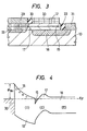
- Fig. 4 shows a band structure diagram illustrative of this state. In Fig. 4, the same parts as in Fig. 3 are indicated by identical symbols.
- Parts indicated by (I), (II) and (III) in Fig. 4 correspond to the layer 12, the layer 17 and a layer 18, respectively.
- the transistor of the present invention has a fundamental structure comprising a source electrode 29 which lies in ohmic contact with the two-dimensional carriers 15, and a gate control electrode 30 which creates or extinguishes the carriers 15, and further the third semiconductor region 18 which is located directly under the control electrode 30 as well as the two-dimensional carriers 15 [in the present case, an n+ GaAs layer having a thickness of about 5000 ⁇ ], and a drain electrode 31 which lies in ohmic contact therewith.
- the essential feature of the transistor operation consists in that the two-dimensional carriers 15 are taken out as current to the n+ layer 18 located vertically below, and that the concentration of the two-dimensional carriers is changed by applying an external potential to the gate electrode 30, whereby the current in the vertical direction is controlled to execute the transistor operation.
- Fig. 4 Shown in Fig. 4 is the energy band diagram directly under the gate electrode in the case of applying no external potential.
- Symbol E F indicates the position of the Fermi energy
- symbol ⁇ Bn denotes the Schottky potential between the gate electrode metal 30 and the Al x Ga 1-x As layer 12. Owing to a phenomenon called the pinning of the Fermi level, the value of ⁇ Bn is considered to hardly change irrespective of the value of the gate voltage.
- Donor ions in a depletion layer under the gate electrode are indicated by numeral 16.
- Fig. 5a Shown in Fig. 5a is the energy band diagram at the time at which the source electrode is grounded to equalize the potentials of a source and a drain, whereupon a gate potential V G positive with respect to the source electrode is applied.
- the two-dimensional carriers 15 at a concentration according to the value of the certain positive gate voltage V G are created. Since the source and the drain are at the same potential, no source-drain current flows in this case.
- the depletion type D-type
- E-type enhancement type
- the threshold potentials of the E-type and D-type are determined by the impurity concentrations and thicknesses of the respective semiconductor layers (I), (II) and (III).
- the layer (II) shall be termed "passage layer”.
- Fig. 6 shown in Fig. 6 is the energy band diagram in the case where a negative gate potential V G is applied to extinguish the two-dimensional carriers. In this case, even when a drain voltage V D is applied, substantially no current flows (except for a breakdown current at the application of a great voltage V D ).
- the transistor can have a great current derived therefrom, will be outlined by comparing this transistor with the selectively-doped heterojunction type FET. Letting L g denote the gate length, and a denote the thickness of the two-dimensional carriers, the current which is L g /a times greater can be taken out. When a is estimated to be 100 ⁇ , the current is about 100 times greater because L g is 1 ⁇ m or so.
- the transistor of the invention when compared with the bipolar transistor, has the important merit that the transistor operation is executed if the thickness of the p-type semiconductor layer 17 is greater than the thickness a of the two-dimensional carriers.
- the restriction which is imposed on the thickness of the base layer is greatly alleviated.
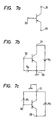
- Fig. 7a The symbols of this transistor are indicated in Fig. 7a.
- Numeral 30 denotes a gate electrode terminal, numeral 29 a source electrode terminal, and numeral 31 a drain electrode terminal.
- the transistor operations explained with reference to Figs. 5a - 5c and Fig. 6 correspond to the case of a grounded source electrode in Fig. 7b.
- a device can of course be fabricated by connecting a drain electrode as in Fig. 7c.
- the two-dimensional carriers to be stored on the heterojunction interface have been electrons.
- the transistor of the present invention can also be fabricated by utilizing positive holes in two dimensions on the basis of the selection of materials for the heterojunction.
- Fig. 8 shows an energy band diagram in the case of a three-layer structure which consists of a p-type GaAs 1-x P x layer 72, an n-type GaAs layer 77 and a p-type GaAs layer 78, a gate electrode 30 being arranged in Schottky contact with the GaAs 1-x P x layer.
- source and drain electrodes are led out from the p-type semiconductors, not from n-type semiconductors, the transistor of the present invention can be fabricated using the two-dimensional holes.
- the present invention is effective with other heterojunctions which meet the condition that the electron gas or positive hole gas in two dimensions can be stored.
- Such systems are, for example, InP-InGaAsP, Al y Ga 1-x As-Al x Ga 1-x As, GaAs-AlGaAsP, InP-InGaAs, InAs-GaAsSb, Al x Ga 1-x As -Ge, GaAs-Ge, CdTe-InSb, and GaSb-InAs.
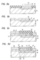
- Figs. 9a - 9d show the principal steps of the manufacture of a semiconductor device which utilizes a two-dimensional electron gas.
- An SiO2 film 40 having a thickness of 5000 ⁇ was evaporated on a semi-insulating GaAs substrate 10 by the use of the CVD process, and was subjected to selective chemical etching in order to form a drain region.
- an Si ion bean 45 was injected at a dose of 2 x 1013 cm-2 under an acceleration voltage of 100 kV, to form the impurity region 18.
- the ion implantation may be performed by selecting the acceleration voltage from within a range of 20 kV to 150 kV and the dose from within a range of 0.5 x 1013 cm ⁇ 2 to 5 x 1013 cm ⁇ 2.
- An SiO2 film was evaporated on the whole surface to a thickness of 5000 ⁇ by CVD, and annealing at 820 °C for 30 minutes was performed to activate the implanted Si atoms (Fig. 9a).
- a GaAs layer 17 was grown by 400 ⁇ at a substrate temperature of 680 °C in a vacuum of 10 ⁇ 11 torr by the use of the molecular beam epitaxy (MBE) process. At that time, the layer was doped with Zn atoms as acceptors to attain an acceptor concentration of 3 x 1017 cm ⁇ 3.
- MBE molecular beam epitaxy
- an Al x Ga 1-x As ( x ⁇ 0.3) layer 12 was grown by 500 ⁇ . At this time, the layer was doped with Si atoms as donors to attain a donor concentration of 1 x 1018 cm ⁇ 3.
- SiO2 33 being 3000 ⁇ thick was evaporated by the CVD process and was selectively subjected to chemical etching, thereby to be windowed for source and drain electrodes. Thereafter, a source/drain metals [AuGe (1000 ⁇ ) - Ni (200 ⁇ ) - Au (1100 ⁇ )] were evaporated (Fig. 9c). Thereafter, alloying was carried out at 450 °C for 3 minutes. Numeral 29 indicates the source electrode, and numeral 31 the drain electrode.
- the source electrode 29 and the drain region 13 are not short-circuited by the diffusion of AuGe.
- the closest distance L SD between the source region and the drain region as indicated in Fig. 9d was about 1 ⁇ m.
- the part of the SiO2 over the drain region 18 was removed, and Ti (1000 ⁇ ) - Pt (200 ⁇ ) - Au (1000 ⁇ ) were evaporated to form a gate electrode 30.
- a two-dimensional electron gas existed at the heterojunction interface of the interspatial part 33 between the source electrode 29 and the gate electrode 30, and this two-dimensional electron gas and the source electrode 29 lay in ohmic contact.
- the p-type region 17 has its concentration lowered down to the order of 1015 cm ⁇ 3.
- the p-type region 17 was as thin as 400 ⁇ , an operating speed which was about 4 times higher than that of a bipolar transistor having a base layer 1000 ⁇ thick and substantially equal dimensions was attained.
- Fig. 10 Shown in Fig. 10 is a case where the transistor of the present invention was performed on a p-type GaAs substrate containing Zn at a concentration of 5 x 1017 cm ⁇ 3, instead of the semi-insulating GaAs substrate.
- the ion implantation process may be employed as in Example 1.
- the thermal diffusion of Si atoms may well be employed for the purpose of improving the crystallinity of epitaxial growth on the drain region 18.
- the major reason therefor is that, when the layer 18 is formed by the ion implantation process, the crystallinity after the annealing worsens in some cases.
- n-type dopant of the buried layer 18 is an n-type dopant whose diffusion coefficient is as small as possible. In case of using the substrate 50 of the p-type, it is important for widening the margin of the transistor operation that depletion layers stretching from a source region and the drain region 18 are prevented from overlapping.
- the semiconductor device was constructed likewise to Example 1.
- Figs. 11a and 11b Shown in Figs. 11a and 11b are examples of principal steps in the case where an E-type transistor and a D-type transistor are properly fabricated on an identical substrate. Drain regions 18, 18', a p-type GaAs layer 17 and an n-type Al x Ga 1-x As layer 12 were formed at thicknesses and impurity concentrations similar to those in Example 1 in advance. Photoresist 49 being about 2 ⁇ m thick was windowed selectively in a part to dispose the gate electrode of the E-type transistor, and Be ions 46 were implanted (at 50) under the conditions of an acceleration voltage of 30 kV and a dose of 1 x 1012 cm ⁇ 2 (Fig. 11a).
- an SiO2 film 3000 ⁇ thick was evaporated by the plasma CVD process, and annealing at 800 °C for 30 minutes was performed to activate the Be atoms. Thereafter, drain electrodes 31, 31', a source electrode 29 and gate electrodes 30, 30' were formed via steps as in Example 1 (Fig. 11b).
- the E-type transistor is a portion having the gate electrode 30'
- the D-type transistor is a portion having the gate electrode 30.
- Threshold potentials can also be adjusted by adjusting the impurity concentrations of the drain regions 18, 18'. That is, in the example of the ion implantation, the threshold value is also changed by changing the implantation energy and the dose.
- Figs. 12a and 12b show an embodiment in the case where an E-type transistor and a D-type transistor are properly fabricated on an identical substrate.
- drain regions 18, 18' were formed on a semi-insulating GaAs substrate 10. Subsequently, a GaAs layer 17' which contained Ge at an acceptor concentration of 5 x 1017 cm ⁇ 3 and which was 500 ⁇ thick was formed by the MBE process. Next, an Al x Ga 1-x As ( x ⁇ 0.3) layer 12' containing Si at a concentration of 7 x 1017 cm ⁇ 3 was grown by 400 ⁇ , and a GaAs layer 34 containing Si at 1018 cm ⁇ 3 was grown by 200 ⁇ (Fig. 12a).
- Numeral 33 designates an insulator layer. Since the distances between the gate electrodes 30, 30' and a channel (namely, the thicknesses of the layers) have a difference, the concentrations of carriers to be induced in the channel become unequal, and the E-type and D-type transistors can be realized.
- Figs. 13a to 13c show examples of steps for fabricating an embodiment of the present invention being of the self-alignment type in such a manner that the E-type and the D-type are formed on an identical substrate.
- n+-type semiconductor layers 18, 18' were formed in a semi-insulating GaAs substrate 10 by the use of the ion implantation of Si.
- a p-type GaAs layer 17'' containing Zn at an acceptor impurity concentration of 5 x 1016 cm ⁇ 3 was grown by 1000 ⁇ by the use of the organic metal vapor evaporation process [OM-VPE process]. More specifically, the V/III ratio between (CH3)3Ga and AsH3 was set at 15, and crystal growth was conducted at a substrate temperature of 700 °C. Dimethyl zinc (CH3)2Zn was used as a p-type dopant.
- an Al x Ga 1-x As ( x ⁇ 0.3) layer 12'' doped with Si at 5 x 1017 cm ⁇ 3 was crystal-grown to a thickness of 600 ⁇ by the OM-VPE process employing AsH3, (CH3)3Ga and (CH3)3Al.
- SiH4 gas was used in order to dope the layer with the donors Si.
- photoresist 49 being about 1.5 ⁇ m thick was deposited and was selectively windowed.
- the photoresist is windowed in a part to form the gate electrode of the D-type.
- Si ions 47' were implanted.
- Conditions for the implantation were an acceleration voltage of 30 kV and a dose of 1 x 1012 cm ⁇ 2 (Fig. 13a).
- Te, Se etc. heavier than Si are sometimes used as ion species.
- a CVD SiO2 film was deposited by 3000 ⁇ , and was annealed at 750 °C for 20 minutes. Thereafter, in order to form drain electrodes, the n-type Al x Ga 1-x As layer 12'' and the p-type GaAs layer 17'' were selectively removed by chemical etching (Fig. 13b). Subsequently, W silicide was deposited on the whole surface by 3000 ⁇ by the use of a vacuum evaporator at 10 ⁇ 6 torr, and gate regions 30, 30' were formed in accordance with conventional processing methods. Next, using the gate electrodes as a mask, Si ions 47 were implanted.
- Conditions for the implantation were an acceleration voltage of 50 kV and a dose of 1 x 1013 cm ⁇ 2.
- SiO2 3000 ⁇ thick was deposited on the whole surface by the CVD process, and it was annealed at 800 °C for 30 minutes. Subsequently, it was etched so as to leave an SiO2 layer 33 for the isolation of electrodes, and a source electrode 29 and the drain electrodes 31, 31' were formed by the use of AuGe (1200 ⁇ )- Ni (150 ⁇ ) - Au (1500 ⁇ ) (Fig. 13c).
- the transistor having the gate electrode 30 is of the E-type, and the transistor having the gate electrode 30' is of the D-type.
- the present embodiment is characterized in that the D-type transistor is fabricated by the ion implantation process.
- the n-type Al x Ga 1-x As layer 12'' may well be replaced with a weak n-type Al x Ga 1-x As layer which is not intentionally doped with any impurity.
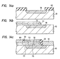
- FIG. 14a to 14c An embodiment in the case of employing two-dimensional positive holes as carriers is shown in Figs. 14a to 14c.
- SiO2 40 of 4000 ⁇ for forming a drain region 78 was deposited on a semi-insulating GaAs substrate 10 and was selectively windowed, whereupon the drain region 78 was formed using the thermal diffusion of Zn.
- diffusion sources As and Zn were placed in an ampoule, and the ampoule was vacuum-sealed. The degree of vacuum was 1 x 10 ⁇ 6 Torr. Thereafter, the diffusion was carried out under the conditions of a diffusion temperature of 650 °C and a diffusion time of 30 minutes. Then, the wafer was taken out of the ampoule and was washed.
- a GaAs layer 77 containing Si at a concentration of 5 x 1017 cm ⁇ 3 was crystal-grown by 800 ⁇ by the use of the MBE process.
- a GaP x As 1-x layer 72 containing Zn at 1 x 1018 cm ⁇ 3 was crystal-grown by 600 ⁇ by the use of the MBE process.
- chemical etching for connecting a drain metal to the p-type GaAs layer 78 was performed (Fig. 14b).
- Au - Zn (99:1) were deposited by 1500 ⁇ as the source/drain metal and were alloyed at 500 °C for 10 minutes, to form a source electrode 89 and a drain electrode 91.
- a gate electrode 30 was formed by the use of Mo (1000 ⁇ ) - Al (2000 ⁇ ).
- SiO2 33 forms spacer layers for isolating the electrodes.
- Ge may well be used in lieu of GaP x As 1-x . More specifically, it is the important point of the present invention that the two-dimensional holes can be accumulated at the heterojunction interface. Even with a heterojunction other than that of the GaP x As 1-x /GaAs or Ge/GaAs system, the transistor of the present invention can be constructed as long as the two-dimensional holes can be stored.
- the isolation between the elements was performed by mesa etching.
- the depth of the etching was approximately 1500 ⁇ - 2000 ⁇ , and caused no hindrance to planar structures.
- the isolation between elements can also be executed by the use of the ion implantation of oxygen atoms etc.
- the second and third semiconductor layers defined a homogenous junction. However, this is not always necessary, but a heterojunction may be used in some cases.
- Example 1 used GaAs as the third semiconductor, a semiconductor greater in the electron affinity than GaAs may well be used. In this case, even when a semiconductor smaller in the electron affinity than GaAs is used, the transistor of the present invention can be performed.
- the important feature of the present invention consists in that two-dimensional electrons or holes stored on a heterojunction interface are caused to flow in a direction perpendicular to the heterojunction interface, thereby to provide a transistor from which a great current can be derived.
Landscapes
- Engineering & Computer Science (AREA)
- Microelectronics & Electronic Packaging (AREA)
- Power Engineering (AREA)
- Physics & Mathematics (AREA)
- Ceramic Engineering (AREA)
- Condensed Matter Physics & Semiconductors (AREA)
- General Physics & Mathematics (AREA)
- Computer Hardware Design (AREA)
- Junction Field-Effect Transistors (AREA)
- Bipolar Transistors (AREA)
Description
- The present invention relates to a semiconductor device, particularly a transistor.
- As transistors which permit high densities of integration on Si substrates, the bipolar transistor and the MOS (Metal-Oxide-Semiconductor) type field effect transistor [MOSFET] have hitherto been typical, in view of the operating principles. While the bipolar transistor is defined as a vertical device which utilizes the physical phenomena of the diffusion and drift of minority carriers, the field effect transistor is a lateral device which utilizes the drive of majority carriers by an electric field.
- In recent years, on account of the limitations of physical constants inherent in Si, ultraspeed devices employing compound semiconductors, principally, gallium-arsenic (GaAs) have been under development without altering the essential mechanisms of transistor operations.
- Among these, a hetero-bipolar transistor (in, for example, Japanese Laid-open Patent Application No. 49-43583) and a selectively doped heterojunction type field effect transistor (in, for example, Japanese Laid-open Patent Application 56-94779) have been described as transistors which employ heterojunctions. From the viewpoint of the operating principle, the latter transistor is almost the same as the MOSFET. In such transistors employing compounds, the essential transistor operations do not differ from those of the devices employing Si, so that disadvantages innate in the bipolar transistor and the field effect transistor (hereinbelow, termed "FET") respectively remain unsolved.
- More specifically, in case of the hetero-bipolar transistor, there is the disadvantage that the density of integration cannot be as high as in the FET because an isolation region must be secured. In the case of the bipolar transistor, there is the lower limit of the thickness of a base layer because of a restriction in the operation principle.
- On the other hand, field effect transistors are well suited for high integration, but a common disadvantage has been the problem that a large current cannot be taken out.
- Fig. 1 shows an energy band gap structure for explaining the operating principle of a prior-art FET of the selectively doped heterojunction type. Similarly, Fig. 2 shows the sectional structure of this FET. Using the molecular beam epitaxy (MBE) process ordinarily, a
GaAs layer 11 which is approximately 1 µm thick and which is not intentionally doped with any impurity (usually, when the MBE is applied, the layer becomes a weak p⁻-type having an impurity concentration of at most 10¹⁵ cm⁻³) is grown on asemi-insulating GaAs substrate 10. Subsequently, an AlxGa1-xAs (x ∼ 0.3)layer 12 which contains approximately 1 x 10¹⁸ cm⁻³ of Si is grown to a thickness of about 500 Å (1Å = 0.1 nm). Thereafter, source anddrain electrodes gate electrode 13 are formed. - Shown in Fig. 1 is the energy band diagram directly under the gate electrode of the semiconductor device. Si atoms introduced by doping are designated at
numeral 14, and a depletion layer based on a Schottky contact is designated atnumeral 16. Since AlGaAs and GaAs have crystal lattices of the same kind and have very close lattice constants, the number of interfacial levels at a heterojunction interface is thought to be very small. GaAs is greater in the electron affinity than AlxGa1-xAs (x ∼ 0.3). Therefore, a potential barrier based on the difference of the electron affinities appears at the heterojunction interface, and carriers in twodimensions 15 are formed. - The known FET described above causes the two-dimensional carriers to flow along the heterojunction interface, and it has accordingly been impossible to derive a great current therefrom.
- EP-A-0084393 discloses a semiconductor device having three semiconductor layers with two of those layers defining a heterojunction. In the device of EP-A-0084393, the two layers defining the heterojunction are the gate and drain layers, and the drain electrode is connected to that layer via further semiconductor layers.
- The present invention seeks to overcome the disadvantages of the known FET of the selectively doped heterojunction type and the hetero-bipolar transistor and proposes a new transistor principle characterised in that the two-
dimensional carriers 15 existing at the heterojunction interface shown in Fig. 1 are taken out to the side ofGaAs layer 11, namely, that they are taken out as current in a direction perpendicular to the heterojunction interface, and that the creation and extinction of the two-dimensional carriers are controlled by a gate voltage, whereby the magnitude of the current is modulated to execute a transistor operation. - According to the present invention there is provided a semiconductor device comprising, at least, a three-layer structure in which a first semiconductor layer and a second semiconductor layer are arranged so as to define a heterojunction and in which the second semiconductor layer and a third semiconductor layer are arranged so as to define a junction, a first electrode which is connected with two-dimensional carriers to appear in the vicinity of said heterojunction interface, a second electrode which is insulated from the two-dimensional carriers and which is electronically connected to said third semiconductor layer and a third electrode serving as control means for the two-dimensional carriers which flow between the first and the second electrodes.
- In general, semiconductor materials which define a heterojunction are used as the different materials of the first and second layers. In addition, the electron affinity of the first semiconductor layer may be selected to be smaller than that of the second semiconductor layer. Accordingly, carriers are induced in the second semiconductor layer at its interface with the first semiconductor layer. The forbidden band width is preferably selected to be greater in the first semiconductor layer than in the second semicomductor layer. As a result, the sum between the electron affinity and band gap of the first semiconductor layer is usually rendered greater than that of the second semiconductor layer.
- Regarding conductivity types, a typical construction is such that the first semiconductor layer is a p-type layer or a non-doped layer which is not intentionally doped with any impuirity, that the second semiconductor layer is an n-type layer or a non-doped layer which is not intentionally doped with any impurity, and that the third semiconductor layer is a p-type layer.
- As the third semiconductor layer, an impurity region may be formed within a semi-insulating semiconductor substrate, or an impurity region may well be provided within a semiconductor substrate identical in the conductivity type to the second semiconductor layer.
- Of course, transistors of both the enhancement type and the depletion type can be fabricated by applying the principle of the present invention. The types can be regulated according to the distance between the gate electrode and the heterojunction interface forming a channel, or the respective impurity concentrations and thicknesses of the first, second and third semiconductor layers.
- Embodiments of the invention are described below by way of example, with reference to the drawings.
- Fig. 1 and Fig. 2 are an energy band diagram and a sectional structural view of a prior-art FET, respectively;
- Fig. 3 and Fig. 4 are a sectional view of a transistor according to the present invention and an energy band diagram under a gate electrode thereof, respectively;
- Figs. 5a - 5c and Fig. 6 are energy band diagrams at the times at which external potentials are applied;
- Figs. 7a - 7c are diagrams for explaining the symbols of transistors of the present invention;
- Fig. 8 is an energy band diagram concerning a transistor of the present invention in the case of utilizing two-dimensional positive holes;
- Figs. 9a - 9d, Fig. 10, Figs. 11a - 11b, Figs. 12a - 12b and Figs. 13a - 13c are sectional views showing processes for fabricating transistors of the present invention in the case of utilizing a two-dimensional electron gas; and
- Figs. 14a - 14c are sectional views of a device in the case of utilizing two-dimensional positive holes.
- First, the operating principle of a new type transistor according to the present invention will be explained with reference to a sectional view [Fig. 3] and an energy band diagram [Fig. 4] of the element, concerning the transistor of the present invention fabricated by employing a heterojunction defined between p-type GaAs and n-type AlxGa1-xAs. Thereafter, operating characteristics in the cases of applying external potentials will be explained.
- As shown in Fig. 3, a p-
type GaAs layer 17 which is about 200 Å to 1000 Å thick and an n-type AlxGa1-xAs (x ∼ 0.3 or so)layer 12 which defines a heterojunction with thelayer 17 and which is about 300 Å to 1000 Å thick are formed on apredetermined semiconductor substrate 10. On account of the difference of electron affinities, free electrons in the AlxGa1-xAs layer are accumulated on a heterojunction interface on the side of the p-type GaAs layer 17, to form anelectron gas layer 15 in two dimensions. Fig. 4 shows a band structure diagram illustrative of this state. In Fig. 4, the same parts as in Fig. 3 are indicated by identical symbols. - Parts indicated by (I), (II) and (III) in Fig. 4 correspond to the
layer 12, thelayer 17 and alayer 18, respectively. - The transistor of the present invention has a fundamental structure comprising a
source electrode 29 which lies in ohmic contact with the two-dimensional carriers 15, and agate control electrode 30 which creates or extinguishes thecarriers 15, and further thethird semiconductor region 18 which is located directly under thecontrol electrode 30 as well as the two-dimensional carriers 15 [in the present case, an n⁺ GaAs layer having a thickness of about 5000 Å], and adrain electrode 31 which lies in ohmic contact therewith. - The essential feature of the transistor operation consists in that the two-
dimensional carriers 15 are taken out as current to the n⁺layer 18 located vertically below, and that the concentration of the two-dimensional carriers is changed by applying an external potential to thegate electrode 30, whereby the current in the vertical direction is controlled to execute the transistor operation. - Shown in Fig. 4 is the energy band diagram directly under the gate electrode in the case of applying no external potential. Symbol EF indicates the position of the Fermi energy, and symbol φBn denotes the Schottky potential between the
gate electrode metal 30 and the AlxGa1-xAslayer 12. Owing to a phenomenon called the pinning of the Fermi level, the value of φBn is considered to hardly change irrespective of the value of the gate voltage. Donor ions in a depletion layer under the gate electrode are indicated bynumeral 16. - Now, the transistor operations in the cases of applying external potentials will be described more in detail with reference to energy band diagrams shown in Figs. 5a, 5b and 5c and Fig. 6. Shown in Fig. 5a is the energy band diagram at the time at which the source electrode is grounded to equalize the potentials of a source and a drain, whereupon a gate potential VG positive with respect to the source electrode is applied. In Fig. 5a, the two-
dimensional carriers 15 at a concentration according to the value of the certain positive gate voltage VG are created. Since the source and the drain are at the same potential, no source-drain current flows in this case. It is the same as in the conventional FET that a case where the two-dimensional carriers are, in effect, existent at VG = 0 is called the depletion type (D-type), while a case where the two-dimensional carriers 15 are induced for the first time after applying a certain positive gate potential is called the enhancement type (E-type). In addition, the threshold potentials of the E-type and D-type are determined by the impurity concentrations and thicknesses of the respective semiconductor layers (I), (II) and (III). Hereinafter, the layer (II) shall be termed "passage layer". - Next, reference is had to the energy band diagrams in the cases where, besides the state of Fig. 5a, a positive drain voltage VD with respect to the source potential is applied [Fig. 5b] and a negative drain voltage VD is applied [Fig. 5c]. In the state of Fig. 5b, the two-
dimensional carriers 15 and free electron carriers in the semiconductor (III) can be taken out as the current between the source and the drain by the effects of diffusion, drift and tunneling. Which of the above three effects predominates is principally determined by the acceptor concentration and thickness of the semiconductor layer (II). In the state of Fig. 5c, the device is turned off. - Next, shown in Fig. 6 is the energy band diagram in the case where a negative gate potential VG is applied to extinguish the two-dimensional carriers. In this case, even when a drain voltage VD is applied, substantially no current flows (except for a breakdown current at the application of a great voltage VD).
- The fact that the transistor can have a great current derived therefrom, will be outlined by comparing this transistor with the selectively-doped heterojunction type FET. Letting Lg denote the gate length, and a denote the thickness of the two-dimensional carriers, the current which is Lg/a times greater can be taken out. When a is estimated to be 100 Å, the current is about 100 times greater because Lg is 1 µm or so.
- On the other hand, when compared with the bipolar transistor, the transistor of the invention has the important merit that the transistor operation is executed if the thickness of the p-
type semiconductor layer 17 is greater than the thickness a of the two-dimensional carriers. Thus, the restriction which is imposed on the thickness of the base layer is greatly alleviated. - The symbols of this transistor are indicated in Fig. 7a.
Numeral 30 denotes a gate electrode terminal, numeral 29 a source electrode terminal, and numeral 31 a drain electrode terminal. The transistor operations explained with reference to Figs. 5a - 5c and Fig. 6 correspond to the case of a grounded source electrode in Fig. 7b. A device can of course be fabricated by connecting a drain electrode as in Fig. 7c. - In the above description of the transistor operations of the present invention, the two-dimensional carriers to be stored on the heterojunction interface have been electrons. The transistor of the present invention can also be fabricated by utilizing positive holes in two dimensions on the basis of the selection of materials for the heterojunction.
- Fig. 8 shows an energy band diagram in the case of a three-layer structure which consists of a p-type GaAs1-xPx layer 72, an n-
type GaAs layer 77 and a p-type GaAs layer 78, agate electrode 30 being arranged in Schottky contact with the GaAs1-xPx layer. Although there is the difference that source and drain electrodes are led out from the p-type semiconductors, not from n-type semiconductors, the transistor of the present invention can be fabricated using the two-dimensional holes. - In the above description, the AlxGa1-xAs/GaAs system has been referred to.
- Needless to say, however, the present invention is effective with other heterojunctions which meet the condition that the electron gas or positive hole gas in two dimensions can be stored.
- Such systems are, for example, InP-InGaAsP, AlyGa1-xAs-AlxGa1-xAs, GaAs-AlGaAsP, InP-InGaAs, InAs-GaAsSb, AlxGa1-xAs -Ge, GaAs-Ge, CdTe-InSb, and GaSb-InAs.
- The effects of the present invention can be summarized as follows:
- (1) Two-dimensional carriers generated at a heterojunction interface are taken out as current in a direction perpendicular to the interface. Therefore, when compared with the prior-art selectively-doped heterojunction FET having substantially equal dimensions, the device of the present invention makes it possible to derive current which is about Lg/a times greater where a denotes the thickness of the two-dimensional carriers and Lg the gate length. At Lg = 1 µm, current which was about 20 times greater could be obtained.
- (2) A passage layer through which the two-dimensional carriers pass in the perpendicular direction can be thinned, in principle, to the thickness of the two-dimensional carriers or so. Therefore, when compared with the bipolar transistor of the same area, the device of the present invention can afford a performance which is 4 - 100 times higher.
- (3) The device of the present invention need not secure an isolation region unlike the case of the bipolar transistor, and is therefore capable of high integration similar to that of the selectively-doped heterojunction type FET.
- (4) When a third semiconductor layer of the n-type or the p-type is selectively formed in a third semiconductor substrate which is semi-insulating, the invention is effective to mitigate the restriction in which a margin in the design of a transistor is determined by the condition that depletion layers extending from both a source region and a drain region do not overlap.
- Figs. 9a - 9d show the principal steps of the manufacture of a semiconductor device which utilizes a two-dimensional electron gas.
- An
SiO₂ film 40 having a thickness of 5000 Å was evaporated on asemi-insulating GaAs substrate 10 by the use of the CVD process, and was subjected to selective chemical etching in order to form a drain region. Using the SiO₂ film as a mask, anSi ion bean 45 was injected at a dose of 2 x 10¹³ cm-² under an acceleration voltage of 100 kV, to form theimpurity region 18. In this regard, the ion implantation may be performed by selecting the acceleration voltage from within a range of 20 kV to 150 kV and the dose from within a range of 0.5 x 10¹³ cm⁻² to 5 x 10¹³ cm⁻². An SiO₂ film was evaporated on the whole surface to a thickness of 5000 Å by CVD, and annealing at 820 °C for 30 minutes was performed to activate the implanted Si atoms (Fig. 9a). - After the SiO₂ film was removed by chemical etching, a
GaAs layer 17 was grown by 400 Å at a substrate temperature of 680 °C in a vacuum of 10⁻¹¹ torr by the use of the molecular beam epitaxy (MBE) process. At that time, the layer was doped with Zn atoms as acceptors to attain an acceptor concentration of 3 x 10¹⁷ cm⁻³. - Next, an AlxGa1-xAs (x ∼ 0.3)
layer 12 was grown by 500 Å. At this time, the layer was doped with Si atoms as donors to attain a donor concentration of 1 x 10¹⁸ cm⁻³. - Subsequently, the selective etching of the AlxGa1-xAs
layer 12 and the p-type GaAs layer 17 for disposing a drain electrode on thedrain region 18 was performed to expose a part of the layer of the drain region 18 (Fig. 9b). - Subsequently,
SiO₂ 33 being 3000 Å thick was evaporated by the CVD process and was selectively subjected to chemical etching, thereby to be windowed for source and drain electrodes. Thereafter, a source/drain metals [AuGe (1000 Å) - Ni (200 Å) - Au (1100 Å)] were evaporated (Fig. 9c). Thereafter, alloying was carried out at 450 °C for 3 minutes.Numeral 29 indicates the source electrode, and numeral 31 the drain electrode. - Here, it is important that the
source electrode 29 and thedrain region 13 are not short-circuited by the diffusion of AuGe. In the current case, the closest distance LSD between the source region and the drain region as indicated in Fig. 9d was about 1 µm. Next, the part of the SiO₂ over thedrain region 18 was removed, and Ti (1000 Å) - Pt (200 Å) - Au (1000 Å) were evaporated to form agate electrode 30. In the current case, a two-dimensional electron gas existed at the heterojunction interface of theinterspatial part 33 between thesource electrode 29 and thegate electrode 30, and this two-dimensional electron gas and thesource electrode 29 lay in ohmic contact. - In case of the present embodiment, owing to the use of the semi-insulating GaAs substrate, a restriction on the source-drain distance LSD is mitigated, and the p-
type region 17 has its concentration lowered down to the order of 10¹⁵ cm⁻³. - Since, in the present embodiment, the p-
type region 17 was as thin as 400 Å, an operating speed which was about 4 times higher than that of a bipolar transistor having a base layer 1000 Å thick and substantially equal dimensions was attained. - Shown in Fig. 10 is a case where the transistor of the present invention was performed on a p-type GaAs substrate containing Zn at a concentration of 5 x 10¹⁷ cm⁻³, instead of the semi-insulating GaAs substrate.
- In order to form an n⁺-
type region 18 in thesemiconductor substrate 50, the ion implantation process may be employed as in Example 1. However, the thermal diffusion of Si atoms may well be employed for the purpose of improving the crystallinity of epitaxial growth on thedrain region 18. - The major reason therefor is that, when the
layer 18 is formed by the ion implantation process, the crystallinity after the annealing worsens in some cases. - As p-type dopants, Be etc. are possible besides Zn.
- Desirable as the n-type dopant of the buried
layer 18 is an n-type dopant whose diffusion coefficient is as small as possible. In case of using thesubstrate 50 of the p-type, it is important for widening the margin of the transistor operation that depletion layers stretching from a source region and thedrain region 18 are prevented from overlapping. - Excepting the selection of the semiconductor substrate, the semiconductor device was constructed likewise to Example 1.
- Shown in Figs. 11a and 11b are examples of principal steps in the case where an E-type transistor and a D-type transistor are properly fabricated on an identical substrate.
Drain regions 18, 18', a p-type GaAs layer 17 and an n-type AlxGa1-xAslayer 12 were formed at thicknesses and impurity concentrations similar to those in Example 1 in advance.Photoresist 49 being about 2 µm thick was windowed selectively in a part to dispose the gate electrode of the E-type transistor, and Beions 46 were implanted (at 50) under the conditions of an acceleration voltage of 30 kV and a dose of 1 x 10¹² cm⁻² (Fig. 11a). After removing the photoresist, an SiO₂ film 3000 Å thick was evaporated by the plasma CVD process, and annealing at 800 °C for 30 minutes was performed to activate the Be atoms. Thereafter,drain electrodes 31, 31', asource electrode 29 andgate electrodes 30, 30' were formed via steps as in Example 1 (Fig. 11b). The E-type transistor is a portion having the gate electrode 30', and the D-type transistor is a portion having thegate electrode 30. Owing to the implantation (50) of the Be ions, the extent of the induction of two-dimensional carriers in this region is adjusted. Threshold potentials can also be adjusted by adjusting the impurity concentrations of thedrain regions 18, 18'. That is, in the example of the ion implantation, the threshold value is also changed by changing the implantation energy and the dose. -
- Figs. 12a and 12b show an embodiment in the case where an E-type transistor and a D-type transistor are properly fabricated on an identical substrate.
- Likewise to Example 1,
drain regions 18, 18' were formed on asemi-insulating GaAs substrate 10. Subsequently, a GaAs layer 17' which contained Ge at an acceptor concentration of 5 x 10¹⁷ cm⁻³ and which was 500 Å thick was formed by the MBE process. Next, an AlxGa1-xAs (x ∼ 0.3) layer 12' containing Si at a concentration of 7 x 10¹⁷ cm⁻³ was grown by 400 Å, and aGaAs layer 34 containing Si at 10¹⁸ cm⁻³ was grown by 200 Å (Fig. 12a). - Next, using a mixture gas consisting of CCl₂F₂ and He, the part of the
GaAs layer 34 corresponding to the gate electrode of the E-type transistor was selectively removed by etching, whereupongate electrodes 30, 30' were formed. The steps of forming asource electrode 29 anddrain electrodes 31, 31' were the same as in Example 1 (Fig. 12b). -
Numeral 33 designates an insulator layer. Since the distances between thegate electrodes 30, 30' and a channel (namely, the thicknesses of the layers) have a difference, the concentrations of carriers to be induced in the channel become unequal, and the E-type and D-type transistors can be realized. -
- Figs. 13a to 13c show examples of steps for fabricating an embodiment of the present invention being of the self-alignment type in such a manner that the E-type and the D-type are formed on an identical substrate.
- Likewise to Example 1, n⁺-type semiconductor layers 18, 18' were formed in a
semi-insulating GaAs substrate 10 by the use of the ion implantation of Si. After annealing, a p-type GaAs layer 17'' containing Zn at an acceptor impurity concentration of 5 x 10¹⁶ cm⁻³ was grown by 1000 Å by the use of the organic metal vapor evaporation process [OM-VPE process]. More specifically, the V/III ratio between (CH₃)₃Ga and AsH₃ was set at 15, and crystal growth was conducted at a substrate temperature of 700 °C. Dimethyl zinc (CH₃)₂Zn was used as a p-type dopant. - Subsequently, an AlxGa1-xAs (x ∼ 0.3) layer 12'' doped with Si at 5 x 10¹⁷ cm⁻³ was crystal-grown to a thickness of 600 Å by the OM-VPE process employing AsH₃, (CH₃)₃Ga and (CH₃)₃Al. In order to dope the layer with the donors Si, SiH₄ gas was used. Next, in order to fabricate the D-type transistor,
photoresist 49 being about 1.5 µm thick was deposited and was selectively windowed. - In the illustration, the photoresist is windowed in a part to form the gate electrode of the D-type. Using the resultant photoresist as a mask, Si ions 47' were implanted. Conditions for the implantation were an acceleration voltage of 30 kV and a dose of 1 x 10¹² cm⁻² (Fig. 13a).
- Te, Se etc. heavier than Si are sometimes used as ion species.
- A CVD SiO₂ film was deposited by 3000 Å, and was annealed at 750 °C for 20 minutes. Thereafter, in order to form drain electrodes, the n-type AlxGa1-xAs layer 12'' and the p-type GaAs layer 17'' were selectively removed by chemical etching (Fig. 13b). Subsequently, W silicide was deposited on the whole surface by 3000 Å by the use of a vacuum evaporator at 10⁻⁶ torr, and
gate regions 30, 30' were formed in accordance with conventional processing methods. Next, using the gate electrodes as a mask,Si ions 47 were implanted. - Conditions for the implantation were an acceleration voltage of 50 kV and a dose of 1 x 10¹³ cm⁻².
- Subsequently, SiO₂ 3000 Å thick was deposited on the whole surface by the CVD process, and it was annealed at 800 °C for 30 minutes. Subsequently, it was etched so as to leave an
SiO₂ layer 33 for the isolation of electrodes, and asource electrode 29 and thedrain electrodes 31, 31' were formed by the use of AuGe (1200 Å)- Ni (150 Å) - Au (1500 Å) (Fig. 13c). - In the current case, the transistor having the
gate electrode 30 is of the E-type, and the transistor having the gate electrode 30' is of the D-type. - The present embodiment is characterized in that the D-type transistor is fabricated by the ion implantation process.
- The reason why the ion implantation was conducted using the gate electrodes as a mask in order to form the source electrode as illustrated in Fig. 13b, is to establish ohmic contact with a two-dimensional electron gas layer at a heterojunction interface under the
gate electrodes 30, 30'. - In the case of the present embodiment where the E-type transistor is previously formed, the n-type AlxGa1-xAs layer 12'' may well be replaced with a weak n-type AlxGa1-xAs layer which is not intentionally doped with any impurity.
- An embodiment in the case of employing two-dimensional positive holes as carriers is shown in Figs. 14a to 14c. SiO₂ 40 of 4000 Å for forming a
drain region 78 was deposited on asemi-insulating GaAs substrate 10 and was selectively windowed, whereupon thedrain region 78 was formed using the thermal diffusion of Zn. For the thermal diffusion of Zn, diffusion sources As and Zn were placed in an ampoule, and the ampoule was vacuum-sealed. The degree of vacuum was 1 x 10⁻⁶ Torr. Thereafter, the diffusion was carried out under the conditions of a diffusion temperature of 650 °C and a diffusion time of 30 minutes. Then, the wafer was taken out of the ampoule and was washed. Subsequently, aGaAs layer 77 containing Si at a concentration of 5 x 10¹⁷ cm⁻³ was crystal-grown by 800 Å by the use of the MBE process. Next, a GaPxAs1-xlayer 72 containing Zn at 1 x 10¹⁸ cm⁻³ was crystal-grown by 600 Å by the use of the MBE process. Next, chemical etching for connecting a drain metal to the p-type GaAs layer 78 was performed (Fig. 14b). Subsequently, Au - Zn (99:1) were deposited by 1500 Å as the source/drain metal and were alloyed at 500 °C for 10 minutes, to form asource electrode 89 and adrain electrode 91. Next, agate electrode 30 was formed by the use of Mo (1000 Å) - Al (2000 Å). - SiO₂ 33 forms spacer layers for isolating the electrodes. For a heterojunction which forms two-dimensional
positive holes 75 to appear at the interface thereof, Ge may well be used in lieu of GaPxAs1-x. More specifically, it is the important point of the present invention that the two-dimensional holes can be accumulated at the heterojunction interface. Even with a heterojunction other than that of the GaPxAs1-x/GaAs or Ge/GaAs system, the transistor of the present invention can be constructed as long as the two-dimensional holes can be stored. - In Examples 1 - 6 described above, the isolation between the elements was performed by mesa etching. The depth of the etching was approximately 1500 Å - 2000 Å, and caused no hindrance to planar structures. Of course, the isolation between elements can also be executed by the use of the ion implantation of oxygen atoms etc.
- In all the above examples, the second and third semiconductor layers defined a homogenous junction. However, this is not always necessary, but a heterojunction may be used in some cases. For example, although Example 1 used GaAs as the third semiconductor, a semiconductor greater in the electron affinity than GaAs may well be used. In this case, even when a semiconductor smaller in the electron affinity than GaAs is used, the transistor of the present invention can be performed.
- The important feature of the present invention consists in that two-dimensional electrons or holes stored on a heterojunction interface are caused to flow in a direction perpendicular to the heterojunction interface, thereby to provide a transistor from which a great current can be derived.
Claims (7)
- A semiconductor device comprising, at least, a three-layer structure in which a first semiconductor layer (12, 12',12'',72) and a second semiconductor layer (17,17',17'',77) are arranged so as to define a heterojunction and in which the second semiconductor layer (17,17',17'',77) and a third semiconductor layer (18,18',78) are arranged so as to define a junction, a first electrode (29,89) which is connected with two-dimensional carriers (15,75) to appear in the vicinity of said heterojunction interface, a second electrode (31,31'91) which is insulated from the two-dimensional carriers (15,75) and which is electronically connected to said third semiconductor layer (18,18',78) , and a third electrode (30,30') serving as control means for the two-dimensional carriers (15,75) which flow between the first and the second electrodes.
- A semiconductor device according to claim 1, wherein the electron affinity of said first semiconductor layer (12,12',12'',72) is smaller than that of said second semiconductor layer (17,17',17'',77).
- A semiconductor device according to claim 1 or claim 2, wherein said first semiconductor layer (12,12',12'') is an n-type semiconductor layer or a semiconductor layer which is not intentionally doped with any impurity (not higher that a concentration of 10¹⁵ cm⁻³), said second semiconductor layer (17,17',17'') is a p-type semiconductor layer or a semiconductor layer which is not intentionally doped with any impurity (not higher than a concentration of 10¹⁵ cm⁻³), and said third semiconductor layer (18,18') is an n-type semiconductor layer.
- A semiconductor device according to claim 1 wherein the sum between an electron affinity and band gap of said first semiconductor layer (12,12',12'',72) is greater than the sum between the electron affinity and band gap of said second semiconductor layer (17,17',17'',77).
- A semiconductor device according to claim 4 wherein said first semiconductor layer (72) is of the p-type or is not intentionally doped with any impurity, said second semiconductor layer (77) is of the n-type or is not intentionally doped with any impurity, and said third semiconductor layer (78) is of the p-type.
- A semiconductor device according to claim 1, wherein said third semiconductor layer (18,18',78) is selectively formed in a semi-insulating substrate (10).
- A semiconductor device according to claim 1, wherein said third semiconductor layer (18,18',78) is selectively formed in a semiconductor substrate (50) which has the same conductivity type as that of said second semiconductor layer (17,17',17'',77).
Applications Claiming Priority (2)
| Application Number | Priority Date | Filing Date | Title |
|---|---|---|---|
| JP58246279A JPH0810763B2 (en) | 1983-12-28 | 1983-12-28 | Semiconductor device |
| JP246279/83 | 1983-12-28 |
Publications (3)
| Publication Number | Publication Date |
|---|---|
| EP0148031A2 EP0148031A2 (en) | 1985-07-10 |
| EP0148031A3 EP0148031A3 (en) | 1987-07-01 |
| EP0148031B1 true EP0148031B1 (en) | 1991-07-17 |
Family
ID=17146171
Family Applications (1)
| Application Number | Title | Priority Date | Filing Date |
|---|---|---|---|
| EP84309131A Expired EP0148031B1 (en) | 1983-12-28 | 1984-12-28 | Semiconductor device |
Country Status (6)
| Country | Link |
|---|---|
| US (1) | US4710787A (en) |
| EP (1) | EP0148031B1 (en) |
| JP (1) | JPH0810763B2 (en) |
| KR (1) | KR920010584B1 (en) |
| CA (1) | CA1222069A (en) |
| DE (1) | DE3484817D1 (en) |
Families Citing this family (14)
| Publication number | Priority date | Publication date | Assignee | Title |
|---|---|---|---|---|
| JPS61174776A (en) * | 1985-01-30 | 1986-08-06 | Sony Corp | Heterojunction field effect transistor |
| JPS61248561A (en) * | 1985-04-25 | 1986-11-05 | インタ−ナショナル・ビジネス・マシ−ンズ・コ−ポレ−ション | Semiconductor structural body |
| US5166083A (en) * | 1991-03-28 | 1992-11-24 | Texas Instruments Incorporated | Method of integrating heterojunction bipolar transistors with heterojunction FETs and PIN diodes |
| US5213987A (en) * | 1991-03-28 | 1993-05-25 | Texas Instruments Incorporated | Method of integrating heterojunction bipolar transistors with PIN diodes |
| US5321427A (en) * | 1992-06-03 | 1994-06-14 | Eastman Kodak Company | Print head modulator |
| JP3272259B2 (en) * | 1997-03-25 | 2002-04-08 | 株式会社東芝 | Semiconductor device |
| US6330261B1 (en) | 1997-07-18 | 2001-12-11 | Cymer, Inc. | Reliable, modular, production quality narrow-band high rep rate ArF excimer laser |
| US6303479B1 (en) * | 1999-12-16 | 2001-10-16 | Spinnaker Semiconductor, Inc. | Method of manufacturing a short-channel FET with Schottky-barrier source and drain contacts |
| US8044432B2 (en) * | 2005-11-29 | 2011-10-25 | The Hong Kong University Of Science And Technology | Low density drain HEMTs |
| US7972915B2 (en) * | 2005-11-29 | 2011-07-05 | The Hong Kong University Of Science And Technology | Monolithic integration of enhancement- and depletion-mode AlGaN/GaN HFETs |
| US7932539B2 (en) * | 2005-11-29 | 2011-04-26 | The Hong Kong University Of Science And Technology | Enhancement-mode III-N devices, circuits, and methods |
| CN101359686B (en) * | 2007-08-03 | 2013-01-02 | 香港科技大学 | Reliable normally-off iii-nitride active device structures, and related methods and systems |
| US8076699B2 (en) * | 2008-04-02 | 2011-12-13 | The Hong Kong Univ. Of Science And Technology | Integrated HEMT and lateral field-effect rectifier combinations, methods, and systems |
| US20100084687A1 (en) * | 2008-10-03 | 2010-04-08 | The Hong Kong University Of Science And Technology | Aluminum gallium nitride/gallium nitride high electron mobility transistors |
Family Cites Families (7)
| Publication number | Priority date | Publication date | Assignee | Title |
|---|---|---|---|---|
| US4141021A (en) * | 1977-02-14 | 1979-02-20 | Varian Associates, Inc. | Field effect transistor having source and gate electrodes on opposite faces of active layer |
| FR2465318A1 (en) * | 1979-09-10 | 1981-03-20 | Thomson Csf | FIELD EFFECT TRANSISTOR WITH HIGH BREAKAGE FREQUENCY |
| CA1145482A (en) * | 1979-12-28 | 1983-04-26 | Takashi Mimura | High electron mobility single heterojunction semiconductor device |
| SE8107136L (en) * | 1980-12-02 | 1982-06-03 | Gen Electric | STEERING ELECTRICAL EQUIPMENT |
| FR2520157B1 (en) * | 1982-01-18 | 1985-09-13 | Labo Electronique Physique | SEMICONDUCTOR DEVICE OF THE HETEROJUNCTION TRANSISTOR TYPE (S) |
| JPS6112081A (en) * | 1984-06-27 | 1986-01-20 | Hitachi Ltd | Semiconductor device |
| JPS6139576A (en) * | 1984-07-31 | 1986-02-25 | Fujitsu Ltd | Semiconductor device |
-
1983
- 1983-12-28 JP JP58246279A patent/JPH0810763B2/en not_active Expired - Lifetime
-
1984
- 1984-12-27 US US06/686,691 patent/US4710787A/en not_active Expired - Fee Related
- 1984-12-27 KR KR1019840008410A patent/KR920010584B1/en not_active IP Right Cessation
- 1984-12-27 CA CA000471031A patent/CA1222069A/en not_active Expired
- 1984-12-28 EP EP84309131A patent/EP0148031B1/en not_active Expired
- 1984-12-28 DE DE8484309131T patent/DE3484817D1/en not_active Expired - Lifetime
Also Published As
| Publication number | Publication date |
|---|---|
| CA1222069A (en) | 1987-05-19 |
| KR920010584B1 (en) | 1992-12-07 |
| JPS60140876A (en) | 1985-07-25 |
| EP0148031A3 (en) | 1987-07-01 |
| EP0148031A2 (en) | 1985-07-10 |
| JPH0810763B2 (en) | 1996-01-31 |
| KR850005165A (en) | 1985-08-21 |
| US4710787A (en) | 1987-12-01 |
| DE3484817D1 (en) | 1991-08-22 |
Similar Documents
| Publication | Publication Date | Title |
|---|---|---|
| US6121153A (en) | Semiconductor device having a regrowth crystal region | |
| US4755857A (en) | Heterostructure semiconductor device | |
| KR100642191B1 (en) | Hetero-junction field effect transistor and process of production of same | |
| EP0148031B1 (en) | Semiconductor device | |
| US8829574B2 (en) | Method and system for a GaN vertical JFET with self-aligned source and gate | |
| EP0114962B1 (en) | Double heterojunction field effect transistors | |
| CN101989601A (en) | Semiconductor device and method for manufacturing same | |
| US20230207636A1 (en) | High Voltage Blocking III-V Semiconductor Device | |
| US4878095A (en) | Semiconductor device in particular a hot electron transistor | |
| KR910002818B1 (en) | Method of manufacturing mes fet | |
| EP0080714B1 (en) | Hetero-junction semiconductor device | |
| EP0130676B1 (en) | Semiconductor device having a hetero junction | |
| KR930011474B1 (en) | Semiconductor device and manufacturing method thereof | |
| US5336626A (en) | Method of manufacturing a MESFET with an epitaxial void | |
| US5351128A (en) | Semiconductor device having reduced contact resistance between a channel or base layer and a contact layer | |
| US5493136A (en) | Field effect transistor and method of manufacturing the same | |
| US11489067B2 (en) | Electron gas transistor, one-piece device comprising at least two transistors in cascode and associated manufacturing methods | |
| US4866491A (en) | Heterojunction field effect transistor having gate threshold voltage capability | |
| US9876082B2 (en) | Transistor with hole barrier layer | |
| EP0131111B1 (en) | Semiconductor device having a heterojunction | |
| EP0437702B1 (en) | Semiconductor integrated circuit of compound semiconductor devices comprising isolation regions and method of making the same | |
| JPS6112081A (en) | Semiconductor device | |
| JPS60136380A (en) | Semiconductor device | |
| JPH06163602A (en) | High-electron-mobility transistor and its manufacture | |
| JPS6184871A (en) | Semiconductor device |
Legal Events
| Date | Code | Title | Description |
|---|---|---|---|
| PUAI | Public reference made under article 153(3) epc to a published international application that has entered the european phase |
Free format text: ORIGINAL CODE: 0009012 |
|
| 17P | Request for examination filed |
Effective date: 19850102 |
|
| AK | Designated contracting states |
Designated state(s): DE FR GB |
|
| PUAL | Search report despatched |
Free format text: ORIGINAL CODE: 0009013 |
|
| RHK1 | Main classification (correction) |
Ipc: H01L 29/76 |
|
| AK | Designated contracting states |
Kind code of ref document: A3 Designated state(s): DE FR GB |
|
| 17Q | First examination report despatched |
Effective date: 19900116 |
|
| GRAA | (expected) grant |
Free format text: ORIGINAL CODE: 0009210 |
|
| AK | Designated contracting states |
Kind code of ref document: B1 Designated state(s): DE FR GB |
|
| REF | Corresponds to: |
Ref document number: 3484817 Country of ref document: DE Date of ref document: 19910822 |
|
| ET | Fr: translation filed | ||
| PLBE | No opposition filed within time limit |
Free format text: ORIGINAL CODE: 0009261 |
|
| STAA | Information on the status of an ep patent application or granted ep patent |
Free format text: STATUS: NO OPPOSITION FILED WITHIN TIME LIMIT |
|
| 26N | No opposition filed | ||
| PGFP | Annual fee paid to national office [announced via postgrant information from national office to epo] |
Ref country code: FR Payment date: 19961128 Year of fee payment: 13 |
|
| PGFP | Annual fee paid to national office [announced via postgrant information from national office to epo] |
Ref country code: GB Payment date: 19961218 Year of fee payment: 13 |
|
| PGFP | Annual fee paid to national office [announced via postgrant information from national office to epo] |
Ref country code: DE Payment date: 19970224 Year of fee payment: 13 |
|
| PG25 | Lapsed in a contracting state [announced via postgrant information from national office to epo] |
Ref country code: GB Free format text: LAPSE BECAUSE OF NON-PAYMENT OF DUE FEES Effective date: 19971228 |
|
| PG25 | Lapsed in a contracting state [announced via postgrant information from national office to epo] |
Ref country code: FR Free format text: THE PATENT HAS BEEN ANNULLED BY A DECISION OF A NATIONAL AUTHORITY Effective date: 19971231 |
|
| GBPC | Gb: european patent ceased through non-payment of renewal fee |
Effective date: 19971228 |
|
| PG25 | Lapsed in a contracting state [announced via postgrant information from national office to epo] |
Ref country code: DE Free format text: LAPSE BECAUSE OF NON-PAYMENT OF DUE FEES Effective date: 19980901 |
|
| REG | Reference to a national code |
Ref country code: FR Ref legal event code: ST |