EP0147697A2 - Ladungsgekoppeltes Bauelement mit steuerbarer Gleichstrom-Eingangsspannung - Google Patents
Ladungsgekoppeltes Bauelement mit steuerbarer Gleichstrom-Eingangsspannung Download PDFInfo
- Publication number
- EP0147697A2 EP0147697A2 EP84114928A EP84114928A EP0147697A2 EP 0147697 A2 EP0147697 A2 EP 0147697A2 EP 84114928 A EP84114928 A EP 84114928A EP 84114928 A EP84114928 A EP 84114928A EP 0147697 A2 EP0147697 A2 EP 0147697A2
- Authority
- EP
- European Patent Office
- Prior art keywords
- register
- charge
- reference register
- input
- signal
- Prior art date
- Legal status (The legal status is an assumption and is not a legal conclusion. Google has not performed a legal analysis and makes no representation as to the accuracy of the status listed.)
- Granted
Links
Images
Classifications
-
- G—PHYSICS
- G11—INFORMATION STORAGE
- G11C—STATIC STORES
- G11C19/00—Digital stores in which the information is moved stepwise, e.g. shift registers
- G11C19/28—Digital stores in which the information is moved stepwise, e.g. shift registers using semiconductor elements
- G11C19/282—Digital stores in which the information is moved stepwise, e.g. shift registers using semiconductor elements with charge storage in a depletion layer, i.e. charge coupled devices [CCD]
- G11C19/285—Peripheral circuits, e.g. for writing into the first stage; for reading-out of the last stage
-
- H—ELECTRICITY
- H10—SEMICONDUCTOR DEVICES; ELECTRIC SOLID-STATE DEVICES NOT OTHERWISE PROVIDED FOR
- H10D—INORGANIC ELECTRIC SEMICONDUCTOR DEVICES
- H10D44/00—Charge transfer devices
- H10D44/40—Charge-coupled devices [CCD]
- H10D44/45—Charge-coupled devices [CCD] having field effect produced by insulated gate electrodes
- H10D44/452—Input structures
-
- H—ELECTRICITY
- H10—SEMICONDUCTOR DEVICES; ELECTRIC SOLID-STATE DEVICES NOT OTHERWISE PROVIDED FOR
- H10D—INORGANIC ELECTRIC SEMICONDUCTOR DEVICES
- H10D84/00—Integrated devices formed in or on semiconductor substrates that comprise only semiconducting layers, e.g. on Si wafers or on GaAs-on-Si wafers
- H10D84/891—Integrated devices formed in or on semiconductor substrates that comprise only semiconducting layers, e.g. on Si wafers or on GaAs-on-Si wafers characterised by the integration of only components covered by H10D44/00, e.g. integration of charge-coupled devices [CCD] or charge injection devices [CID
Definitions
- the present invention relates generally to charge coupled devices (CCD's) with registers, such as CCD delay lines, for transferring electrical charges. More particularly, the invention relates to an input structure for CCD's capable of automatic adjustment of a DC. input bias charge.
- CCD's charge coupled devices
- registers such as CCD delay lines
- CCD delay lines have come to be widely used in television sets and the like for delay processing.
- CCD delay lines are used for delay processing of analog signals, such as video signals.
- a DC input bias charge is commonly applied to an input section to which input signals for the CCD delay line are applied.
- this input bias is provided by external amplitude control of some sort.
- the external control is adjusted to apply a bias charge at a predetermined level to the input section of the CCD.
- the input bias level tends to fluctuate due to variations in the temperature-dependent characteristics of the input section.
- difficulties have been encountered in accurately adjusting the input bias charge by means of the external amplitude control.
- US-A 4,139,784 discloses an.CCD input circuit capable of adjusting the DC input bias to a CCD signal register serving as a CCD delay line. Feedback control of the DC input bias is performed by comparing the electric charge transferred through a reference register with a constant reference signal from a reference voltage source.
- the difficulty mentioned above cannot be avoided even with this structure since adjustment of the reference voltage from the reference voltage source would still be necessary.
- Another object of the invention is to provide an input structure for a charge coupled device which can eliminate the influence of temperature variations on them input bias.
- a CCD system is provided with a reference voltage source which produces a reference signal to be compared with the electric charge transferred through a reference register.
- the input bias on the reference register is feedback-controlled in accordance with difference between the charge transferred through the reference register and the reference signal value.
- the operating conditions of the reference voltage source are adjusted to match those of the reference register so that the reference signal value varies in accordance with the operating conditions of the reference register.
- the reference voltage source comprises another reference register rated at a given fraction of the maximum charge value of the reference register.
- the input section of the reference register is coupled to the input section of a CCD signal register to apply substantially the same input bias to the latter as is applied to the former.
- a charge coupled device comprises a signal register for transferring input electric charges therethrough, the signal register having an input section, a first reference register having an input section of substantially the same structure as the input section of the signal register, the first reference register transferring electric charges from its input section to its output section, a feedback circuit connected to the first reference register to receive an electric voltage substantially corresponding to the electric charge transferred through the first reference register, the feedback circuit comparing the electric voltage with a reference voltage which varies solely as a function of the environmental conditions of the first reference register, deriving a feedback signal, and applying the feedback signal to the first reference register for feedback controlling a bias on the first reference register to a given fraction of a maximum charge rating of the first reference register, and means for coupling the signal register to the first reference register for setting a DC input bias of the signal register to substantially the same bias as the first reference register.
- a charge coupled device with automatic adjustment of a DC input bias comprises a signal register adapted to transfer input electric charges, a first reference register adapted to transfer electric charges from its input section to its output section, the first reference register having a first maximum charge rating, a common input gate bridging the signal register and the first reference register, a second reference register constantly supplied with a voltage substantially corresponding to a second maximum charge rating of the second reference register, the second maximum charge rating being a given fraction of the first maximum charge rating, a common output gate bridging the first and second reference registers, and a feedback circuit comparing a first charge transferred through the first reference register and a second charge transferred through the second reference register, deriving a feedback signal having a value corresponding to the difference between the first and second charges, and feedback-controlling an input bias on the first reference register to the given fraction of the first maximum charge rating, thereby feedback-controlling an DC input bias on the signal register to substantially the same charge level as that on the first reference register.
- a charge coupled device comprises a semiconductor substrate, a first register formed on the semiconductor substrate and adapted to transfer signal charges in a given direction therethrough, a second register formed on the semiconductor substrate for charge transfer in the given direction and having substantially the same input structure as the first register, a third register formed on the semiconductor substrate for charge transfer in the given direction and having an output structure substantially the same as that of the second register, the maximum charge rating of the third register being a given fraction of the maximum charge rating of the second register, a plurality of electrodes formed on the first, second and third registers for driving the transference of charges through each of the registers and/or accumulating charges therein, and means for detecting charges output by the second and third registers and adjusting the charges to be transferred through the second and third registers to the respective output charges.
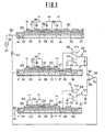
- Figs. 1 and 2 illustrate the preferred embodiment of a charge coupled device system (CCD system) of the present invention in terms of a CCD delay line employing a two-phase, -buried-channel device with two-level, n-channel gate electrodes.
- the CCD system has a P-type silicon substrate 10 common to a signal register (CCD delaying) 12, a first reference register 14 and a second reference register 16.
- the signal register 12 has a channel width a and a desired number of gates.
- the first reference register 14 has substantially the same channel width a as of the signal register 12 and a predetermined channel length l .
- the second reference register 16 has substantially the same channel length l as first reference register 14.
- the input end section 18 of the second reference register 16 has a channel width a/2, i. e . only half of that of the first reference register 14 and a predetermined channel length l 1 .
- the output end section 20 of the 'second reference register 16 has the same channel width as the other two registers 12, 14 and a predetermined channel length l 2 .
- the input and output end channels of register 16 are joined by a section of tapering width.
- the channels of registers 12, 14 and 16 are ribbons of N-type doped silicon sandwiched between the P-type 'silicon substrate 10 and an insulating layer 27 of silicon dioxide.
- CCD's can be of either surface- or buried- channel type and can be driven by any of a number of control signal phasing schemes. It should also be appreciated that other electrode structures, such as single-layer or triple- layer, may be employed, and metal and polysilicon electrodes may be employed.
- the signal register 12 has a source region 22 which comprises an N + diffusion in the P-type silicon substrate 10.
- the signal register 12 also has first and second input polysilicon gate electrodes 24 and 26 deposited on the insulating layer 27 and mutually insulated by an interleaved insulating layer 32 of silicon dioxide.
- the signal register 12 also has a plurality of first- level electrodes 28 and a plurality of second-level electrodes 30 all of polysilicon and mutually insulated by Si0 2 layers 32.
- the first and second input gate electrodes 24 and 26 extend over the channel of the first reference register 14 so that they also serve as input gate ; electrodes for the latter.
- the first- and second-level electrodes 28 and 30 extend over both the first and second reference registers 14 and 16 to serve in pairs as shift-staging electrodes for each.
- the first reference register 14 has a source region 34 which is similar to that in the signal register 12 and comprises an N + diffusion in P-type silicon substrate 10.
- the first reference register 14 also has a N + floating diffusion region 36 and another N + diffusion region used as a pre-charge drain region 38 following the floating diffusion region 36 but separated from the latter by a short section of a channel.
- the first reference register 14 also has an output gate 40 42, both of polysilicon deposited on the Si0 2 insulator 27.
- the output gate 40 and the pre-charge gate 42 also extend over the second reference register 16 so as to serve as output gate and the pre-charge gate for the latter.
- the second reference register 16 also has a source region 44 comprising an N + diffusion region in the P-type silicon substrate 10.
- the source region 44 is similar geometrically to the source regions of the signal register 12 and the first reference register 14.
- the second reference register 16 also has a N + floating diffusion region 46 which is similar to that with reference number 36 in the first reference reqister14.
- a pre-charge drain region 48 in the second reference register 16 correcponding to that with the reference number 38 in the first register 14 is similarly separated from the floating diffusion region 46 by a short section of a channel.
- First-level and second-level transfer electrodes 50 and 52 are also formed on the third register 16.
- the first- and second-level transfer electrodes 50 and 52 made of polysilicon, are located at positions corresponding to the first and second input gate electrodes 24 and 26 of the signal register 12 and the first reference register 14.
- the operating states of the two switches 54 and 70 control the charge on the floating diffusion regions 36 and 46, respectively.
- the pre-charge drain regions 38 and 48 serve to drain the charge floating diffusion regions 36 and 46, respectively at a timing in synchronism with operation of the switches 54 and 70. For instance, an electric charge or a potential in the floating diffusion regions 36 and 46 are reset to +V DD as constantly applied to the pre-charge drain region 38 and 48 when a resetting clock is applied to the pre-charge gate 42.
- the resetting clock to be applied to the pre-charge gate 42 is to be produced at a timing synchronized with the opening of the switches 54 and 70 with a given substantially short delay.
- the potential in the floating diffusion regions 36 and 46 is reset to +V DD .
- the floating diffusion region 36 is connected to the inverting input terminal 56 of a differential amplifier 58 via a source follower amplifier 60 and a switch 54.
- the source follower 60 comprises two source-drain-connected MOS FET's 62 and 64.
- the switch 54 is represented by a manual-throw switch symbol in the drawings, it may be and usually will be a MOS FET switch.
- the second floating diffusion region 46 is also connected to the positive or non-inverting input terminal 66 of the differential amplifier 58 via a source follower 68 and a switch 70.
- the source follower 68 comprises MOS FET 72 and 74.
- the symbolically illustrated switch 70 will in practice be a MOS FET.
- the switch ON-timing of the switches 54 and 70 are controlled by a sample/hold signal to pass the voltage corresponding to the transferred charge through the first and second registers 14 and 16.
- the sample/hold signal may provide a duty cycle for controlling the switch ON-timing in synchronism with the transfer of the charge through the registers 14 and 16. Therefore, the signalling timing would by synchronized with the signalling timing of the clocks ⁇ 1 and ⁇ 2 .
- the output terminal 76 of differential amplifier 58 is connected directly to the source region 34 of the first reference register 14 and to the source region 22 via a resistor 77.
- the source region 22 is also connected in parallel with resistor 77 to a signal source 78 via a capacitor 80.
- the resistor 77 is inserted to isolate the signal source 78 from the differential amplifier 58 and the first reference register 14.
- the source followers 60 and 80, switches 54 and 70, the differential amplifier 58, the resistor 77 and the capacitor 80 may be formed on the same chip as the registers 10, 14 and 16.
- a power source 82 is connected to the source region 44 of the second reference register 16.
- the power source 82 is rated so as to keep the electric charge in the source region 44 saturated, in other words, to keep its potential on full carrier charged level.
- the first-level electrodes 28 and 50 cooperate with the adjacent second-level electrodes 30 and 52 to drive electric charges from potential well to potential well along the buried channels.
- each electric charge packet is determined by the potential difference between adjacent potential wells which in turn is determined by the voltage levels of the two-phase clock signals (0 1 , ⁇ 2 ) coupled to a battery 84 as well as other operating signals described later. That is, electric charge packets migrate among the asymmetrical potential wells at the various gates and electrodes until they find the local potential minima or voltage maxima.
- Each electric charge thus transferred through the second reference register 16 and output through the floating diffusion region 46 is converted into a corresponding voltage by the source follower 68.
- the converted voltage is sample-held by the switch 70.
- the switch 70 thus supplies a voltage corresponding to the maximum charge rating of the second reference register 16 to the positive input terminal 66 of the differential amplifier 58. Since the source region 44 of the second reference register 16 is always saturated, the voltage applied to the positive input terminal 66 of the differential amplifier 58 constantly corresponds to the full rating of the second reference register 16.
- the input voltage at the negative input terminal 56 of the differential amplifier 58 is zero, since there is no electric charge transferred to the floating diffusion region 36 of the first reference register 14.
- the output voltage of the differential amplifier 58 corresponds to the maximum charge rating of the second reference register 16.
- the output voltage of the differential amplifier 58 serves as a feedback voltage for the first reference register 14.
- the feedback voltage from the differential amplifier 58 increases the "depth" of the potential well at the source region 34 of the first reference register 14 by an amount corresponding to the feedback voltage, which, in turn, corresponds to the full rated charge of the second reference register 16.
- the second reference register 16 Since the second reference register 16 has the first-level and second-level transfer electrodes 28 and 30 and the output gate electrode 40 in common to the first reference register 14, charge transfer is performed in the second reference register 16 at substantially the same timing as in the first reference register 14. As set forth above, the charge applied to the source region 44 of the second reference register 16 corresponds to its maximum charge rating. Therefore, when a charge corresponding to the depth of the potential well in the source region 34 of the first reference register 14 is transferred to the floating diffusion region 36, the charge corresponding to the maximum charge rating of the second reference register 16 is transferred to the floating diffusion region 46 of the second reference register 16. Source followers 60 and 68 operate concurrently to convert the charge in the floating diffusion regions 36 and 46 into voltages. The switches 54 and 70 also operate concurrently. As a result, a voltage corresponding to the maximum charge rating of the second reference register 16 is applied to the positive input terminal 66 of the differential amplifier 58 simultaneously with the voltage from the switch 54.
- the differential amplifier 58 outputs through its output terminal 76 a voltage corresponding to the difference between the input voltages.
- the output voltage of the differential amplifier 58 is fed back to the source region 34 of the first reference register 14.
- the feedback voltage from the differential amplifier 58 adjusts the depth of the potential well of the source region 34, specifically such that the difference between the input voltages of the differential amplifier 58 is reduced to zero. As a result, the charge transferred through the first reference register 14 is held as close as possible to the full charge transferred through the second reference register 16.
- this feedback control causes the charge transferred through the first reference register 14 to match the charge output of the second - reference register 16, i.e., the maximum charge rating of the second reference register 16.
- the width of the input end section 18 of the second reference register 16 is half that of the first reference register 14, and thus the maximum charge rating of the first reference register 14 is twice that of the second reference register 16. Since the charge transferred through the first reference register 14 is feedback controlled to correspond to the maximum handling charge of the second reference register, the first reference register 14 handles half (1/2) of its maximum charge rating. In other words, the first reference register 14 operates under a bias of 1/2 of its maximum charge rating.
- the first reference register 14 employs the first and second input gate electrodes 24 and 26 in common with the signal register 12. Also, as set forth above, the first reference register 14 has the same channel width a as the signal register 12 and the structure of the source region 34 matches that of the source region 22 of the signal register 12.
- the signal register 12 has substantially the same input structure as the first reference register.
- the bias condition of the signal register 12 will always be substantially equal to that of the first reference register 14.
- the bias on the signal register 12 substantially corresponds to 1/2 of the maximum charge rating of the first reference register 14.
- the signal register will operate at the center of its dynamic range, which is specially advantageous when the input from the signal source 78 is in the form of a sine-wave.
- the DC bias on the signal register 12 can be automatically controlled to the center (1/2) of its dynamic range. Therefore, according to the shown embodiment, it is no longer necessary to employ a conventional amplitude control for adjustment of the DC bias on the signal register. Furthermore, it is also unnecessary to manually adjust the DC bias on the signal register, as the DC bias can be automatically controlled.
- the first reference register 14 since the first reference register 14 has substantiall game input structure as the signal register 12 and has substantially same output structure as that of the second reference register 16, the input section of the first reference register 14 will be influenced by the same temperature variation as that subject to the input section of the signal register 12.
- the output section of the first register 14 will be subject to the influences of the same temperature variations as the output section of the second output register 16.
- the bias on the first reference register 14 can be maintained accurately t 1/2 its maximum charge rating.
- the DC input bias on the signal register 12 can be constantly maintained at 1/2 the maximum charge rating irrespective of temperature variations.
- the photo-mask pattern used during the exposure process in semi-conductor IC fabrication process should be designed to have an input channel of the proper width.
- the DC bias level can be set with very high accuracy simply by proper design of the photo-mask pattern. This production process also ensures good reproducability.
- the first-level transfer electrodes 28 and the second-level transfer electrodes 30 can conveniently be formed in common with all three registers 12, 14 and 16. Additionally, this allows the first and second input electrodes 24 and 26 of the signal register 12 and the first reference register 14 to be conveniently formed in common. Similarly, the output gate electrode 40 and the pre-charge gate 42 of the first and second reference register 14 and 16 can be formed in common.
- the invention is not limited to this specific level, but rather can be selected to be any arbitrary value. It is only necessary to select the width of the second reference register in relation to the width of the first reference register to obtain the desired level of DC input bias. For instance, if a DC input bias lying at 3/4 of the maximum charge rating or if a dynamic range is preferred, as shown in Fig. 5, then the width of the input end section 18 of the second reference register 16 should be 3a/4, where a is the channel width of the first reference register 14 and the signal register 12. In this case, the input bias will be clamped at the voltage level of 3/4 of the dynamic range of the signal register.
- the charge transferred through the first and second reference registers 14 and 16 are output to the source followers 60 and 68 through the floating diffusions regions 36 and 46 and then input to the input terminals 56 and 66 of the 'differential amplifier 58.
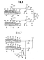
- thestructure shown in Fig. 6, for example, may be used instead.
- N + floating gates 100 and 102 made of polysilicon are formed on the P-type silicon substrate 10.
- the floating gates 100 and 102 are connected to the source followers 60 and 68, respectively.
- Reset switches 104 are connected to the floating gates 100 and 102 to control their potentials.
- the charges at the floating gates 100 and 102 are fed to the corresponding input terminals 56 and 66 of the differential amplifier in the form of voltages corresponding to the respective charges via the source followers 6 0 and 68.
- the output of the differential amplifier 58 is fed back to the first reference register 14 to control the bias thereof and accordingly the DC input bias on the signal register.
- F ig. 7 shows a further embodiment of the CCD system according to the present invention.
- the pre-charge drain regions 38 and 48 are connected to power source V DD via resistors 110 and 112.
- the input terminals 56 and 66 of the differential amplifier 58 are connected between the pre-charge drain gates 38 and 48 and the resistors 110 and 112, respectively.
- the differential amplifier compares the voltage drops respectively effected by the pre-charge drain regions 38 and 48.
- the output of the differential amplifier 58 is used as a feedback signal to feedback control the bias on the first reference register 14 to the desired fraction of its maximum charge rate. As a result, the DC input bias on the signal register 12 can be controlled automatically.
- the shown embodiments employ a diode cut-off system for inputting signals to the source regions 22, 34 and 44 of the signal register 12 and the first and second reference registers 14 and 16 by exerting a voltage on the source region
- other input systems such as a potential-balance system
- the connections to the differential amplifier should be adapted accordingly so that the charge transferred through the first reference register can be constantly and automatically controlled to 1/2 of its maximum charge rate.
- the present invention should be understood as to include all of the possible embodiments and modifications providing for the same or similar effects to those illustrated hereabove.
- the invention should not be understood as being specifically for application to a two-phase, buried-channel CCD device with two-level, n-channel gate electrodes but should be appreciated to include various types of CCD systems including surface-channel types as well as buried-channel types, and with any practically reasonable number of clock phases.
Landscapes
- Solid State Image Pick-Up Elements (AREA)
- Television Signal Processing For Recording (AREA)
- Processing Of Color Television Signals (AREA)
Applications Claiming Priority (2)
| Application Number | Priority Date | Filing Date | Title |
|---|---|---|---|
| JP58232586A JPH0721960B2 (ja) | 1983-12-09 | 1983-12-09 | テレビジョン信号の遅延装置 |
| JP232586/83 | 1983-12-09 |
Publications (3)
| Publication Number | Publication Date |
|---|---|
| EP0147697A2 true EP0147697A2 (de) | 1985-07-10 |
| EP0147697A3 EP0147697A3 (en) | 1987-04-15 |
| EP0147697B1 EP0147697B1 (de) | 1991-02-27 |
Family
ID=16941676
Family Applications (1)
| Application Number | Title | Priority Date | Filing Date |
|---|---|---|---|
| EP84114928A Expired EP0147697B1 (de) | 1983-12-09 | 1984-12-07 | Ladungsgekoppeltes Bauelement mit steuerbarer Gleichstrom-Eingangsspannung |
Country Status (4)
| Country | Link |
|---|---|
| EP (1) | EP0147697B1 (de) |
| JP (1) | JPH0721960B2 (de) |
| CA (1) | CA1234917A (de) |
| DE (1) | DE3484190D1 (de) |
Cited By (3)
| Publication number | Priority date | Publication date | Assignee | Title |
|---|---|---|---|---|
| FR2604820A1 (fr) * | 1986-10-01 | 1988-04-08 | Sony Corp | Dispositif a couplage de charge comportant un moyen particulier de detection de charge |
| EP0394017A3 (de) * | 1989-04-18 | 1991-06-12 | Sony Corporation | Ladungsschieberegister mit verbesserter Eingangsstruktur |
| US5210777A (en) * | 1989-04-17 | 1993-05-11 | Sony Corporation | Charge coupled device having switched inverting and non-inverting input signal paths, input biassing circuit and temperature compensation |
Family Cites Families (2)
| Publication number | Priority date | Publication date | Assignee | Title |
|---|---|---|---|---|
| US4139784A (en) * | 1977-08-02 | 1979-02-13 | Rca Corporation | CCD Input circuits |
| JPH041960A (ja) * | 1990-04-18 | 1992-01-07 | Matsushita Electric Ind Co Ltd | テープレコーダのブレーキ機構 |
-
1983
- 1983-12-09 JP JP58232586A patent/JPH0721960B2/ja not_active Expired - Lifetime
-
1984
- 1984-12-06 CA CA000469477A patent/CA1234917A/en not_active Expired
- 1984-12-07 DE DE8484114928T patent/DE3484190D1/de not_active Expired - Lifetime
- 1984-12-07 EP EP84114928A patent/EP0147697B1/de not_active Expired
Cited By (4)
| Publication number | Priority date | Publication date | Assignee | Title |
|---|---|---|---|---|
| FR2604820A1 (fr) * | 1986-10-01 | 1988-04-08 | Sony Corp | Dispositif a couplage de charge comportant un moyen particulier de detection de charge |
| US5210777A (en) * | 1989-04-17 | 1993-05-11 | Sony Corporation | Charge coupled device having switched inverting and non-inverting input signal paths, input biassing circuit and temperature compensation |
| EP0394017A3 (de) * | 1989-04-18 | 1991-06-12 | Sony Corporation | Ladungsschieberegister mit verbesserter Eingangsstruktur |
| US5086440A (en) * | 1989-04-18 | 1992-02-04 | Sony Corporation | Charge coupled device with enhanced input structure |
Also Published As
| Publication number | Publication date |
|---|---|
| EP0147697A3 (en) | 1987-04-15 |
| JPH0721960B2 (ja) | 1995-03-08 |
| JPS60124097A (ja) | 1985-07-02 |
| DE3484190D1 (de) | 1991-04-04 |
| CA1234917A (en) | 1988-04-05 |
| EP0147697B1 (de) | 1991-02-27 |
Similar Documents
| Publication | Publication Date | Title |
|---|---|---|
| US4139784A (en) | CCD Input circuits | |
| EP0324456B1 (de) | Ausgangsschaltung einer Ladungsschiebeanordnung | |
| EP0192142A1 (de) | Ladungsverschiebeanordnung | |
| US5029189A (en) | Input structure for charge coupled devices with controllable input bias | |
| US3784847A (en) | Dielectric strip isolation for jfet or mesfet depletion-mode bucket-brigade circuit | |
| US4627082A (en) | Semiconductor device for obtaining an accurate threshold voltage adjustment | |
| EP0147697A2 (de) | Ladungsgekoppeltes Bauelement mit steuerbarer Gleichstrom-Eingangsspannung | |
| EP0161023B1 (de) | Ladungsgekoppelte Halbleiteranordnung mit dynamischer Steuerung | |
| US4272693A (en) | Analysis circuit for a charge coupled device | |
| US4700085A (en) | Circuit for detecting signal charges transferred in a charge transfer device | |
| USRE31612E (en) | CCD Input circuits | |
| US5086440A (en) | Charge coupled device with enhanced input structure | |
| US4165537A (en) | Analog charge transfer apparatus | |
| EP0415852B1 (de) | Eingangsschaltung für CCD-Verzögerungsleitung | |
| US5177772A (en) | Charge coupled device with enhanced input structure | |
| US4374334A (en) | Signal comparator apparatus | |
| US5381177A (en) | CCD delay line capable of automatic adjustment of an input bias voltage to charge transfer regions | |
| US5294817A (en) | Output circuit for charged transfer device and having a high detection sensitivity | |
| US4350902A (en) | Input stage for a monolithically integrated charge transfer device which generates two complementary charge packets | |
| JP2569501B2 (ja) | 電荷結合装置 | |
| US4627084A (en) | Differentiation and integration utilizing charge-coupled devices | |
| US4412344A (en) | Integrated rectifier circuit | |
| JP2513190B2 (ja) | 電荷結合装置 | |
| KR950008677B1 (ko) | 반도체신호 전하 검출장치 | |
| US4524450A (en) | Automatic adjustment of the amplitudes of plural-phase CCD clocking voltages |
Legal Events
| Date | Code | Title | Description |
|---|---|---|---|
| PUAI | Public reference made under article 153(3) epc to a published international application that has entered the european phase |
Free format text: ORIGINAL CODE: 0009012 |
|
| 17P | Request for examination filed |
Effective date: 19841207 |
|
| AK | Designated contracting states |
Designated state(s): DE FR GB NL |
|
| PUAL | Search report despatched |
Free format text: ORIGINAL CODE: 0009013 |
|
| AK | Designated contracting states |
Kind code of ref document: A3 Designated state(s): DE FR GB NL |
|
| 17Q | First examination report despatched |
Effective date: 19890323 |
|
| GRAA | (expected) grant |
Free format text: ORIGINAL CODE: 0009210 |
|
| AK | Designated contracting states |
Kind code of ref document: B1 Designated state(s): DE FR GB NL |
|
| REF | Corresponds to: |
Ref document number: 3484190 Country of ref document: DE Date of ref document: 19910404 |
|
| ET | Fr: translation filed | ||
| PLBE | No opposition filed within time limit |
Free format text: ORIGINAL CODE: 0009261 |
|
| STAA | Information on the status of an ep patent application or granted ep patent |
Free format text: STATUS: NO OPPOSITION FILED WITHIN TIME LIMIT |
|
| 26N | No opposition filed | ||
| REG | Reference to a national code |
Ref country code: GB Ref legal event code: IF02 |
|
| PGFP | Annual fee paid to national office [announced via postgrant information from national office to epo] |
Ref country code: GB Payment date: 20031203 Year of fee payment: 20 |
|
| PGFP | Annual fee paid to national office [announced via postgrant information from national office to epo] |
Ref country code: NL Payment date: 20031205 Year of fee payment: 20 |
|
| PGFP | Annual fee paid to national office [announced via postgrant information from national office to epo] |
Ref country code: FR Payment date: 20031210 Year of fee payment: 20 |
|
| PGFP | Annual fee paid to national office [announced via postgrant information from national office to epo] |
Ref country code: DE Payment date: 20031218 Year of fee payment: 20 |
|
| PG25 | Lapsed in a contracting state [announced via postgrant information from national office to epo] |
Ref country code: GB Free format text: LAPSE BECAUSE OF EXPIRATION OF PROTECTION Effective date: 20041206 |
|
| PG25 | Lapsed in a contracting state [announced via postgrant information from national office to epo] |
Ref country code: NL Free format text: LAPSE BECAUSE OF EXPIRATION OF PROTECTION Effective date: 20041207 |
|
| REG | Reference to a national code |
Ref country code: GB Ref legal event code: PE20 |
|
| NLV7 | Nl: ceased due to reaching the maximum lifetime of a patent |
Effective date: 20041207 |