EP0146967A2 - Photoconductive target of image pickup tube and manufacturing method thereof - Google Patents
Photoconductive target of image pickup tube and manufacturing method thereof Download PDFInfo
- Publication number
- EP0146967A2 EP0146967A2 EP84116346A EP84116346A EP0146967A2 EP 0146967 A2 EP0146967 A2 EP 0146967A2 EP 84116346 A EP84116346 A EP 84116346A EP 84116346 A EP84116346 A EP 84116346A EP 0146967 A2 EP0146967 A2 EP 0146967A2
- Authority
- EP
- European Patent Office
- Prior art keywords
- layer
- photoconductive
- cadmium
- evaporated
- target
- Prior art date
- Legal status (The legal status is an assumption and is not a legal conclusion. Google has not performed a legal analysis and makes no representation as to the accuracy of the status listed.)
- Granted
Links
Images

Classifications
-
- H—ELECTRICITY
- H01—ELECTRIC ELEMENTS
- H01J—ELECTRIC DISCHARGE TUBES OR DISCHARGE LAMPS
- H01J29/00—Details of cathode-ray tubes or of electron-beam tubes of the types covered by group H01J31/00
- H01J29/02—Electrodes; Screens; Mounting, supporting, spacing or insulating thereof
- H01J29/10—Screens on or from which an image or pattern is formed, picked up, converted or stored
- H01J29/36—Photoelectric screens; Charge-storage screens
- H01J29/39—Charge-storage screens
- H01J29/45—Charge-storage screens exhibiting internal electric effects caused by electromagnetic radiation, e.g. photoconductive screen, photodielectric screen, photovoltaic screen
-
- H—ELECTRICITY
- H01—ELECTRIC ELEMENTS
- H01J—ELECTRIC DISCHARGE TUBES OR DISCHARGE LAMPS
- H01J9/00—Apparatus or processes specially adapted for the manufacture, installation, removal, maintenance of electric discharge tubes, discharge lamps, or parts thereof; Recovery of material from discharge tubes or lamps
- H01J9/20—Manufacture of screens on or from which an image or pattern is formed, picked up, converted or stored; Applying coatings to the vessel
- H01J9/233—Manufacture of photoelectric screens or charge-storage screens
Definitions
- the present invention relates to a photoconductive target of an image pickup tube and, more particularly to a target having a high photo-sensitivity even in an infrared range and a manufacturing method thereof.
- Image pickup tubes which utilize cadmium selenide (CdSe) as a material for a photoconductive layer of a target, e.g., " Chalnicon" (trade mark; available from TOSHIBA), are commercially available.
- the target of such an image pickup tube has a multilayer structure consisting of a CdSe layer and a high resistance layer of arsenic sulfide (As 2 S 3 ) or arsenic selenide (As 2 Se3 deposited thereon. Since the target has a quantum efficiency of about 1 in the visible light range and therefore has a high sensitivity, "Chalnicon" is very suitable for a monochrome or a color image pickup tube.
- An example of an image pickup tube target having a high sensitivity in the infrared region is disclosed in Japanese Patent Disclosure No. 57-208041.
- This target has an evaporated layer which consists of a mixture of CdSe and CdTe and has CdSe as its major component.
- this target does not have a satisfactory dark current characteristic and a sufficient photo-sensitivity in a long wavelength region.
- the photoconductive target of the image pickup tube comprises a transparent substrate, a transparent electro-conductive layer formed on the transparent substrate, a photoconductive layer containing Cd, Te and Se as its major components and formed on the conductive layer, ano a high resistance layer formed on the photoconductive layer.
- the molar ratios of Cd, Te and Se contained in the photoconductive layer satisfy a general formula CdTe 1-x Se x where x falls within the range between 0.3 and 0.5.
- the photoconductive layer described above can be essentially formed of a mixture of CdTe and CdSe, or can have a structure in which CdTe and CdSe are alternately deposited.
- the photoconductive layer can contain a crystal growth promotor such as CuC1 or CdC12'
- a method of manufacturing the photoconductive target of the image pickup tube according to the present invention comprises the steps of:
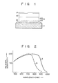
- a photoconductive target comprises a transparent substrate 11 such as a glass face plate, a transparent electro-conductive layer 12 such as a SnO 2 or In 2 0 3 film formed directly on the substrate 11 or through a transparent film such as a color filter, a photoconductive layer 15 of a mixture of CdTe and CdSe formed on the layer 12, a high resistance layer 16 comprising an evaporated layer of diarsenic triselenide (As 2 Se 3 ) or diarsenic trisulfide (As 2 S 3 ) and formed on the layer 15, and a high resistance layer 17 comprising an evaporated layer of diantimony trisulfide (Sb2S3) and formed on the layer 16.
- the photoconductive layer 15 comprises a first evaporated layer 13 and a second evaporated layer 14. Note that another high resistance layer of, e.g., Si0 2 , Ce0 2 or Al 2 O 3 can be formed between the transparent conductive layer 12 and the first evaporated layer 13.
- the first evaporated layer 13 has a thickness of 200 to 2,000 A
- the second evaporated layer 14 has a thickness larger than that of the layer 13, i.e., 0.3 to 1.8 ⁇ m.
- the first and second evaporated layers 13 and 14 are deposited in different deposition atmospheres, as will be described later.
- a total thickness of the first and second evaporated layers 13 and 14 is 0.5 to 2.0 ⁇ m.
- a thickness of the high resistance layer 16 is about 1.0 to 2.0 ⁇ m, e.g., 1.5 ⁇ m.
- a thickness of the high resistance layer 17 is about 500 to 1,500 A, e.g., 1,000 ⁇ .
- the transparent electro-conductive layer 12 is deposited on the transparent substrate 11 by a conventional method.
- the photoconductive layer 15 of CdTe and CdSe is deposited on the layer 12.
- the photoconductive layer 15 is deposited by evaporating CdTe and CdSe in an argon gas atmosphere at a pressure of 1.3 to 130 Pa and at a substrate temperature of 150 to 250°C. Evaporation of CdTe and CdSe is performed in the following manner.
- a CdTe powder and a CdSe powder are mixed at molar ratios which satisfy the above general formula and the resulting mixture is subjected to a heat treatment so as to form a solid solution.
- the solid solution is used as an evaporation source.
- CdTe and CdSe can be simultaneously evaporated using them as separate evaporation sources, or can be alternately deposited in a multilayer. In this case, molar ratios of Cd, Te and Se must satisfy the above formula.
- the first evaporated layer 13 is deposited to a thickness of about 1,000 ⁇ by the above deposition method.
- the second evaporated layer 14 is deposited to a thickness of about 9,000 A under the same condictions as described above except that the evaporation atmosphere is changed to an argon gas atmosphere containing oxygen.
- the target is then sintered in an inert gas, e.g., nitrogen gas, atmosphere containing Te vapor at a temperature of 550 to 650°C for about 20 minutes.
- an inert gas e.g., nitrogen gas, atmosphere containing Te vapor at a temperature of 550 to 650°C for about 20 minutes.
- the high resistance layer 16 of As 2 Se 3 is deposited on the sintered photoconductive layer 15 to a thickness of about 1.5 ⁇ m, and the high resistance layer 17 formed of Sb2S3 having a thickness of about 1,000 A is deposited thereon so as to obtain a photoconductive target of a multilayer structure.
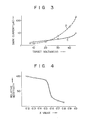
- Fig. 2 is a graph showing a comparison of the spectral sensitivities of the photoconductive target of the present invention and that of the prior art disclosed in Japanese Patent Disclosure No. 57-208C41.
- a curve A represents a spectral sensitivity of the target of the present invention in which the general formula CdTe 1-x Se x is satisfied when an x value is 0.4
- a curve B represents the spectral sensitivity of the target of the prior art when the x value is 0.7.
- a sufficient photo-sensitivity can be obtained in an infrared region up to a wavelength of about 900 nm, and is therefore an improvement with respect to the prior art.
- the difference in the photo-sensitivities of both the targets is attributable to a difference in the x values.
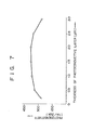
- Fig. 3 is a graph showing a change in dark current characteristics resulting from different manufacturing processes of the photoconductive layer of the targer.
- a curve C represents the dark current characteristics of the target formed by a process of the present invention in which the photoconductive layer is formed first in argon atmosphere and then in argon atmospheres containing oxygen.
- a curve D represents the dark current characteristics of the target in which the photoconductive layer is formed only in argon atmosphere containing oxygen..As is apparent from the graph in Fig. 3, the dark current characteristics of the target obtained by the process of the present invention are improved.
- oxygen gas influences a porosity of the utoconductive layer, resulting in a change in crystal growth occurring during a sintering operation.
- the present inventors examined various characteristics of the target when the x value in the formula CdTe 1-x Se x representing the composition of the photoconductive layer was varied. It was found that when the x value falls within the range between 0.3 and 0.5, satisfactory photo-sensitivity, dark current characteristics and after-image characteristics can be obtained. The results are described hereinafter.
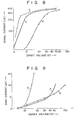
- Fig. 4 is a graph showing a change in the photo-sensitivity when the x value is varied.
- the photo-sensitivity abruptly decreases when the x value exceeds 0.5. This is because a crystal structure is changed in accordance with changes in the x values.
- the present inventors observed the crystal structure of the photoconductive layer upon varying the x value. When the x value was below 0.5, the crystal structure of the photoconductive layer became a zincblende type which has a uniform crystal orientation. On the contrary, when the x value exceeded 0.5, the crystal structure does not have a uniform crystal orientation.
- Fig. 5 is a graph showing a change in a dark current when the x value is changed. As is apparent from this graph, when the x value exceeds about 0.5, the dark current abruptly increases. On the other hand, even when the x value is less than 0.3, the dark current gradually increases. This is because the resistance of the photoconductive layer is decreased and electrons are injected from the transparent conductive layer when the x value is below 0.3. Note that these values are measured when the target voltage is 15 V.
- Fig. 6 is a graph showing a change in an after-image fading-out voltage when the x value is changed.
- the after-image fading-out voltage is a target voltage necessary for fading out the after-image.
- the x value is outside the range between 0.3 and 0.5, the after-image fading-out voltage increases. This can be caused by a poor crystal property and an injection of electrons from the transparent conductive layer.
- a preferable thickness of the photoconductive layer of the target according to the present invention will be describec hereinafter.
- Fig. 7 is a graph showing a change in the photo-sersitivity in a wavelength near 900 nm when a thickness of the photoconductive layer is varied.
- the thickness of the photoconcuctive layer is less than 0.5 ⁇ m, the photo-sensitivity is undesireably low.
- the thickness of the layer is too small, e.g., less than 0.5 ⁇ m, light in a long wavelength region is partially transmitted through the photoconductive layer and reaches the high resistance layer. Therefore, when light is excessively irradiated, the after-image characteristic is degraded considerably.
- the thickness of the photoconductive layer preferably falls within the range between 0.5 and 2.0 pm.
- Figs. 8 and 9 are graphs showing changes in signal and dark currents with respect to the target voltage.
- curves E, F and G respectively show the case when the thickness of the photoconductive layer is set at 0.3 ⁇ m, 1 ⁇ m and 3 ⁇ m.
- the thickness of the photoconductive layer is set at 0.3 ⁇ m, 1 ⁇ m and 3 ⁇ m.
- the thickness of the photoconductive layer is set at 0.3 ⁇ m, good kick-off characteristics of the sensitivity can be obtained, but the dark current characteristics are degraded.
- the thickness of the layer is 3 ⁇ m, the after-image fading-out voltage considerably increases and the sensitivity is degraded.
- the photoconductive target according to the present invention has good photo-sensitivity and dark current characteristics.
Abstract
Description
- The present invention relates to a photoconductive target of an image pickup tube and, more particularly to a target having a high photo-sensitivity even in an infrared range and a manufacturing method thereof.
- Image pickup tubes which utilize cadmium selenide (CdSe) as a material for a photoconductive layer of a target, e.g., "Chalnicon" (trade mark; available from TOSHIBA), are commercially available. The target of such an image pickup tube has a multilayer structure consisting of a CdSe layer and a high resistance layer of arsenic sulfide (As2S3) or arsenic selenide (As 2 Se3 deposited thereon. Since the target has a quantum efficiency of about 1 in the visible light range and therefore has a high sensitivity, "Chalnicon" is very suitable for a monochrome or a color image pickup tube. However, in "Chalnicon", the limit of spectral sensitivity of long wavelengths is close to 700 nm, and photo-sensitivity in the infrared region exceeding this limit is insufficient. When an image pickup operation is performed at low illuminance, e.g., for monitoring roads at night, the interior of tunnels or warehouses, an image pickup tube having a high sensitivity, not only in the visible light region but also in the infrared region, must be used. Therefore, a demand for such an image pickup tube has arisen.
- An example of an image pickup tube target having a high sensitivity in the infrared region is disclosed in Japanese Patent Disclosure No. 57-208041. This target has an evaporated layer which consists of a mixture of CdSe and CdTe and has CdSe as its major component. However, this target does not have a satisfactory dark current characteristic and a sufficient photo-sensitivity in a long wavelength region.
- It is an object of the present invention to provide a photoconductive target of an image pickup tube which has high photo-sensitivity even in a long wavelength region of 800 nm or more, and a good, dark current characteristic.
- It is another object of the present invention to provide a method of manufacturing the photoconductive target of the image pickup tube as described above.
- The photoconductive target of the image pickup tube, according to the present invention, comprises a transparent substrate, a transparent electro-conductive layer formed on the transparent substrate, a photoconductive layer containing Cd, Te and Se as its major components and formed on the conductive layer, ano a high resistance layer formed on the photoconductive layer. The molar ratios of Cd, Te and Se contained in the photoconductive layer satisfy a general formula CdTe1-xSex where x falls within the range between 0.3 and 0.5.
- The photoconductive layer described above can be essentially formed of a mixture of CdTe and CdSe, or can have a structure in which CdTe and CdSe are alternately deposited.
- The photoconductive layer can contain a crystal growth promotor such as CuC1 or CdC12'
- A method of manufacturing the photoconductive target of the image pickup tube according to the present invention comprises the steps of:
- forming a transparent electro-conductive layer on a transparent substrate;
- depositing a mixture containing Cd, Te and Se onto the conductive layer in an inert gas atmosphere so as to form a first evaporated layer containing Cd, Te and Se as major components, the molar ratios of Cd, Te and Se satisfying a general formula CdTe1-xSex (where x = 0.3 to 0.5);
- depositing the mixture on the first evaporated layer in an inert gas atmosphere containing oxygen so as to form a second evaporated layer having a thickness larger than that of said first evaporated layer and containing Cd, Te and Se as major components, the molar ratios of Cd, Te and Se satisfying said general formula;
- heat-treating the first and second evaporated layers in an inert gas atmosphere at a temperature of 550 to 650°C, thereby forming a photoconductive layer; and
- forming a high resistance layer on the photoconductive layer.
- This invention can be more fully understood from the following detailed description when taken in conjunction with the accompanying drawings, in which:
- Fig. 1 is a sectional view of a photoconductive target of an image pickup tube according to an embodiment of the present invention;
- Fig. 2 is a graph representing a spectral sensitivity of the photoconductive target;
- Fig. 3 is a graph showing τhe relationship between a target voltage and a dark current of the photoconductive target;
- Fig. 4 is a graph showing the relationship between an x value and a photo-sensitivity of the photoconductive target;
- Fig. 5 is a graph showing the relationship between the x value and the dark current of the photoconductive target;
- Fig. 6 is a graph showing the relationship .between the x value and a sticking-vanishing voltage of the photoconductive target;
- Fig. 7 is a graph showing the relationship between a thickness of the photoconductive target and the photo-sensitivity thereof;
- Fig. 8 is a graph showing the relationship between the target voltage and a signal current of the photoconductive target; and
- Fig. 9 is a graph showing the relationship between the target voltage and the dark current of the photoconductive target.
- An embodiment of the present invention will be described with reference to the accompanying drawings.
- As shown in Fig. 1, a photoconductive target according to the embodiment of the present invention comprises a
transparent substrate 11 such as a glass face plate, a transparent electro-conductive layer 12 such as a SnO2 or In203 film formed directly on thesubstrate 11 or through a transparent film such as a color filter, aphotoconductive layer 15 of a mixture of CdTe and CdSe formed on thelayer 12, ahigh resistance layer 16 comprising an evaporated layer of diarsenic triselenide (As2Se3) or diarsenic trisulfide (As2S3) and formed on thelayer 15, and ahigh resistance layer 17 comprising an evaporated layer of diantimony trisulfide (Sb2S3) and formed on thelayer 16. Thephotoconductive layer 15 comprises a firstevaporated layer 13 and a second evaporated layer 14. Note that another high resistance layer of, e.g., Si02, Ce02 or Aℓ2O3 can be formed between the transparentconductive layer 12 and the first evaporatedlayer 13. - The
photoconductive layer 15 contains Cd, Te and Se as major components and has a composition represented by a general formula CdTe1-xSex (x = 0.3 to 0.5). Therefore, in the general formula CdTe1-xSex, Te is 0.5 to 0.7 and Se is 0.3 to 0.5 when Cd is 1. The first evaporatedlayer 13 has a thickness of 200 to 2,000 A, and the second evaporated layer 14 has a thickness larger than that of thelayer 13, i.e., 0.3 to 1.8 µm. The first and second evaporatedlayers 13 and 14 are deposited in different deposition atmospheres, as will be described later. A total thickness of the first and second evaporatedlayers 13 and 14 is 0.5 to 2.0 µm. A thickness of thehigh resistance layer 16 is about 1.0 to 2.0 µm, e.g., 1.5 µm. A thickness of thehigh resistance layer 17 is about 500 to 1,500 A, e.g., 1,000 Å. - A preferred method of manufacturing the photoconductive target as described above will be described hereinafter.
- The transparent electro-
conductive layer 12 is deposited on thetransparent substrate 11 by a conventional method. Thephotoconductive layer 15 of CdTe and CdSe is deposited on thelayer 12. Thephotoconductive layer 15 is deposited by evaporating CdTe and CdSe in an argon gas atmosphere at a pressure of 1.3 to 130 Pa and at a substrate temperature of 150 to 250°C. Evaporation of CdTe and CdSe is performed in the following manner. A CdTe powder and a CdSe powder are mixed at molar ratios which satisfy the above general formula and the resulting mixture is subjected to a heat treatment so as to form a solid solution. The solid solution is used as an evaporation source. Alternatively, CdTe and CdSe can be simultaneously evaporated using them as separate evaporation sources, or can be alternately deposited in a multilayer. In this case, molar ratios of Cd, Te and Se must satisfy the above formula. - The first evaporated
layer 13 is deposited to a thickness of about 1,000 Å by the above deposition method. Subsequently, the second evaporated layer 14 is deposited to a thickness of about 9,000 A under the same condictions as described above except that the evaporation atmosphere is changed to an argon gas atmosphere containing oxygen. - The target is then sintered in an inert gas, e.g., nitrogen gas, atmosphere containing Te vapor at a temperature of 550 to 650°C for about 20 minutes. The
high resistance layer 16 of As2Se3 is deposited on the sinteredphotoconductive layer 15 to a thickness of about 1.5 µm, and thehigh resistance layer 17 formed of Sb2S3 having a thickness of about 1,000 A is deposited thereon so as to obtain a photoconductive target of a multilayer structure. - Characteristics of the photoconductive target of the image pickup tube according to the present invention will be described hereinafter.
- Fig. 2 is a graph showing a comparison of the spectral sensitivities of the photoconductive target of the present invention and that of the prior art disclosed in Japanese Patent Disclosure No. 57-208C41.
- In Fig. 2, a curve A represents a spectral sensitivity of the target of the present invention in which the general formula CdTe1-xSex is satisfied when an x value is 0.4, and a curve B represents the spectral sensitivity of the target of the prior art when the x value is 0.7. As is apparent from the graph in Fig. 2, with the target of the present invention, a sufficient photo-sensitivity can be obtained in an infrared region up to a wavelength of about 900 nm, and is therefore an improvement with respect to the prior art. The difference in the photo-sensitivities of both the targets is attributable to a difference in the x values.
- Fig. 3 is a graph showing a change in dark current characteristics resulting from different manufacturing processes of the photoconductive layer of the targer. In Fig. 3, a curve C represents the dark current characteristics of the target formed by a process of the present invention in which the photoconductive layer is formed first in argon atmosphere and then in argon atmospheres containing oxygen. A curve D represents the dark current characteristics of the target in which the photoconductive layer is formed only in argon atmosphere containing oxygen..As is apparent from the graph in Fig. 3, the dark current characteristics of the target obtained by the process of the present invention are improved. Although the reason is clearly analyzed, it is surmised that oxygen gas influences a porosity of the utoconductive layer, resulting in a change in crystal growth occurring during a sintering operation.
- The present inventors examined various characteristics of the target when the x value in the formula CdTe1-xSex representing the composition of the photoconductive layer was varied. It was found that when the x value falls within the range between 0.3 and 0.5, satisfactory photo-sensitivity, dark current characteristics and after-image characteristics can be obtained. The results are described hereinafter.
- Fig. 4 is a graph showing a change in the photo-sensitivity when the x value is varied. As is apparent from this graph, the photo-sensitivity abruptly decreases when the x value exceeds 0.5. This is because a crystal structure is changed in accordance with changes in the x values. The present inventors observed the crystal structure of the photoconductive layer upon varying the x value. When the x value was below 0.5, the crystal structure of the photoconductive layer became a zincblende type which has a uniform crystal orientation. On the contrary, when the x value exceeded 0.5, the crystal structure does not have a uniform crystal orientation.
- Fig. 5 is a graph showing a change in a dark current when the x value is changed. As is apparent from this graph, when the x value exceeds about 0.5, the dark current abruptly increases. On the other hand, even when the x value is less than 0.3, the dark current gradually increases. This is because the resistance of the photoconductive layer is decreased and electrons are injected from the transparent conductive layer when the x value is below 0.3. Note that these values are measured when the target voltage is 15 V.
- Fig. 6 is a graph showing a change in an after-image fading-out voltage when the x value is changed. Note that the after-image fading-out voltage is a target voltage necessary for fading out the after-image. As is apparent from the graph, when the x value is outside the range between 0.3 and 0.5, the after-image fading-out voltage increases. This can be caused by a poor crystal property and an injection of electrons from the transparent conductive layer.
- A preferable thickness of the photoconductive layer of the target according to the present invention will be describec hereinafter.
- Fig. 7 is a graph showing a change in the photo-sersitivity in a wavelength near 900 nm when a thickness of the photoconductive layer is varied. As can be seen from this graph, when the thickness of the photoconcuctive layer is less than 0.5 µm, the photo-sensitivity is undesireably low. When the thickness of the layer is too small, e.g., less than 0.5 µm, light in a long wavelength region is partially transmitted through the photoconductive layer and reaches the high resistance layer. Therefore, when light is excessively irradiated, the after-image characteristic is degraded considerably. On the other hand, when the thickness of the photoconductive layer exceeds 2 µm, the after-image fading-out voltage abruptly increases and undesirably exceeds a value at which the structure is damaged. For this reason, a margin of the target voltage is reduced. Therefore, the thickness of the photoconductive layer preferably falls within the range between 0.5 and 2.0 pm.
- Figs. 8 and 9 are graphs showing changes in signal and dark currents with respect to the target voltage. In Figs. 8 and 9, curves E, F and G respectively show the case when the thickness of the photoconductive layer is set at 0.3 µm, 1 µm and 3 µm. As is apparent from Figs. 8 and 9, when the thickness of the photoconductive layer is 0.3 µm, good kick-off characteristics of the sensitivity can be obtained, but the dark current characteristics are degraded. When the thickness of the layer is 3 µm, the after-image fading-out voltage considerably increases and the sensitivity is degraded.
- These results are measured using a standard light source at a color temperature of 2,850 K with an illuminance of 1 lux.
- As described above, the photoconductive target according to the present invention has good photo-sensitivity and dark current characteristics.
Claims (11)
Applications Claiming Priority (2)
| Application Number | Priority Date | Filing Date | Title |
|---|---|---|---|
| JP58245181A JPS60140636A (en) | 1983-12-28 | 1983-12-28 | Photoconductive target of image pick-up tube and its manufacture |
| JP245181/83 | 1983-12-28 |
Publications (3)
| Publication Number | Publication Date |
|---|---|
| EP0146967A2 true EP0146967A2 (en) | 1985-07-03 |
| EP0146967A3 EP0146967A3 (en) | 1986-08-06 |
| EP0146967B1 EP0146967B1 (en) | 1988-03-30 |
Family
ID=17129815
Family Applications (1)
| Application Number | Title | Priority Date | Filing Date |
|---|---|---|---|
| EP84116346A Expired EP0146967B1 (en) | 1983-12-28 | 1984-12-27 | Photoconductive target of image pickup tube and manufacturing method thereof |
Country Status (4)
| Country | Link |
|---|---|
| US (1) | US4614891A (en) |
| EP (1) | EP0146967B1 (en) |
| JP (1) | JPS60140636A (en) |
| DE (1) | DE3470250D1 (en) |
Families Citing this family (8)
| Publication number | Priority date | Publication date | Assignee | Title |
|---|---|---|---|---|
| JPH0762986B2 (en) * | 1987-01-14 | 1995-07-05 | 株式会社日立製作所 | Light receiving device |
| JP2001284628A (en) * | 2000-03-29 | 2001-10-12 | Shindengen Electric Mfg Co Ltd | X-ray detector |
| WO2014121187A2 (en) | 2013-02-01 | 2014-08-07 | First Solar, Inc. | Photovoltaic device including a p-n junction and method of manufacturing |
| US11876140B2 (en) | 2013-05-02 | 2024-01-16 | First Solar, Inc. | Photovoltaic devices and method of making |
| CN104183663B (en) | 2013-05-21 | 2017-04-12 | 第一太阳能马来西亚有限公司 | Photovoltaic device and manufacturing method thereof |
| US10062800B2 (en) | 2013-06-07 | 2018-08-28 | First Solar, Inc. | Photovoltaic devices and method of making |
| US9871154B2 (en) | 2013-06-21 | 2018-01-16 | First Solar, Inc. | Photovoltaic devices |
| US10529883B2 (en) | 2014-11-03 | 2020-01-07 | First Solar, Inc. | Photovoltaic devices and method of manufacturing |
Citations (3)
| Publication number | Priority date | Publication date | Assignee | Title |
|---|---|---|---|---|
| US3486059A (en) * | 1966-01-11 | 1969-12-23 | Tokyo Shibaura Electric Co | High sensitivity photoconductor for image pickup tube |
| JPS57208041A (en) * | 1981-06-16 | 1982-12-21 | Toshiba Corp | Photoconductive target and its manufacture |
| JPS58216341A (en) * | 1982-06-08 | 1983-12-16 | Toshiba Corp | Photoconductive target for camera tube |
Family Cites Families (8)
| Publication number | Priority date | Publication date | Assignee | Title |
|---|---|---|---|---|
| US28156A (en) * | 1860-05-08 | Wringing clothes | ||
| US3872344A (en) * | 1972-09-15 | 1975-03-18 | Tokyo Shibaura Electric Co | Image pickup tube |
| JPS5118155A (en) * | 1974-08-03 | 1976-02-13 | Matsushita Electric Ind Co Ltd | Datsusuikitono anzensochi |
| US3947717A (en) * | 1975-03-31 | 1976-03-30 | Rca Corporation | Photoconductor of cadmium selenide and aluminum oxide |
| JPS5814753B2 (en) * | 1976-01-19 | 1983-03-22 | 株式会社東芝 | photoconductive target |
| JPS5342610A (en) * | 1976-09-30 | 1978-04-18 | Fujitsu Ltd | Talkie transmission system on digital telephone exchange |
| JPS5826832B2 (en) * | 1978-01-20 | 1983-06-06 | 株式会社東芝 | Method for manufacturing photoconductive targets |
| JPS54122988A (en) * | 1978-03-17 | 1979-09-22 | Toshiba Corp | Manufacture for photo conductive target |
-
1983
- 1983-12-28 JP JP58245181A patent/JPS60140636A/en active Granted
-
1984
- 1984-12-26 US US06/686,401 patent/US4614891A/en not_active Expired - Fee Related
- 1984-12-27 EP EP84116346A patent/EP0146967B1/en not_active Expired
- 1984-12-27 DE DE8484116346T patent/DE3470250D1/en not_active Expired
Patent Citations (3)
| Publication number | Priority date | Publication date | Assignee | Title |
|---|---|---|---|---|
| US3486059A (en) * | 1966-01-11 | 1969-12-23 | Tokyo Shibaura Electric Co | High sensitivity photoconductor for image pickup tube |
| JPS57208041A (en) * | 1981-06-16 | 1982-12-21 | Toshiba Corp | Photoconductive target and its manufacture |
| JPS58216341A (en) * | 1982-06-08 | 1983-12-16 | Toshiba Corp | Photoconductive target for camera tube |
Non-Patent Citations (2)
| Title |
|---|
| PATENTS ABSTRACTS OF JAPAN, vol. 7, no. 62 (E-164) [1207], 15th March 1983; & JP-A-57 208 041 (TOKYO SHIBAURA DENKI K.K.) 21-12-1982 * |
| PATENTS ABSTRACTS OF JAPAN, vol. 8, no. 66 (E-234) [1503], 28th March 1984; & JP-A-58 216 341 (TOKYO SHIBAURA DENKI K.K.) 16-12-1983 * |
Also Published As
| Publication number | Publication date |
|---|---|
| DE3470250D1 (en) | 1988-05-05 |
| EP0146967B1 (en) | 1988-03-30 |
| JPS60140636A (en) | 1985-07-25 |
| JPH0554211B2 (en) | 1993-08-12 |
| EP0146967A3 (en) | 1986-08-06 |
| US4614891A (en) | 1986-09-30 |
Similar Documents
| Publication | Publication Date | Title |
|---|---|---|
| US4040985A (en) | Photoconductive films | |
| EP0146967B1 (en) | Photoconductive target of image pickup tube and manufacturing method thereof | |
| Thomsen et al. | High‐Sensitivity Photoconductor Layers | |
| US4675092A (en) | Method of producing thin film electroluminescent structures | |
| US4007473A (en) | Target structures for use in photoconductive image pickup tubes and method of manufacturing the same | |
| GB1475723A (en) | Photoconductive target of an image pickup tube and method for manufacturing the same | |
| EP0298745B1 (en) | Thin film electroluminescent device | |
| US4759951A (en) | Heat-treating Cd-containing photoelectric conversion film in the presence of a cadmium halide | |
| EP0047651B1 (en) | Method of producing image sensor | |
| US3486059A (en) | High sensitivity photoconductor for image pickup tube | |
| CA1086547A (en) | Photoconductor element with superimposed layers of ca te and zn te containing in | |
| Kraus et al. | Cd x Hg1− x Te Films by Cathodic Sputtering | |
| EP0162310B1 (en) | Photoconductive target of the image pickup tube | |
| US4406050A (en) | Method for fabricating lead halide sensitized infrared photodiodes | |
| US3816787A (en) | Photoconductor comprising cadmium selenide | |
| US4442446A (en) | Sensitized epitaxial infrared detector | |
| EP0140246B1 (en) | A thin film electroluminescent display device | |
| US4883562A (en) | Method of making a photosensor | |
| US3985918A (en) | Method for manufacturing a target for an image pickup tube | |
| Fujiwara et al. | The heterojunction ZnSe-(Zn1− xCdxTe) 1− y (In2Te3) y having high sensitivity in the visible light range and its applications | |
| US4866332A (en) | Target of image pickup tube | |
| JPS5826832B2 (en) | Method for manufacturing photoconductive targets | |
| US4445131A (en) | Photoconductive image pick-up tube target | |
| JPH0151016B2 (en) | ||
| JPS5816288B2 (en) | Kodo Denta Getsutono Seizouhouhou |
Legal Events
| Date | Code | Title | Description |
|---|---|---|---|
| PUAI | Public reference made under article 153(3) epc to a published international application that has entered the european phase |
Free format text: ORIGINAL CODE: 0009012 |
|
| 17P | Request for examination filed |
Effective date: 19841227 |
|
| AK | Designated contracting states |
Designated state(s): DE FR GB |
|
| PUAL | Search report despatched |
Free format text: ORIGINAL CODE: 0009013 |
|
| AK | Designated contracting states |
Kind code of ref document: A3 Designated state(s): DE FR GB |
|
| 17Q | First examination report despatched |
Effective date: 19870317 |
|
| GRAA | (expected) grant |
Free format text: ORIGINAL CODE: 0009210 |
|
| AK | Designated contracting states |
Kind code of ref document: B1 Designated state(s): DE FR GB |
|
| REF | Corresponds to: |
Ref document number: 3470250 Country of ref document: DE Date of ref document: 19880505 |
|
| ET | Fr: translation filed | ||
| PLBE | No opposition filed within time limit |
Free format text: ORIGINAL CODE: 0009261 |
|
| STAA | Information on the status of an ep patent application or granted ep patent |
Free format text: STATUS: NO OPPOSITION FILED WITHIN TIME LIMIT |
|
| 26N | No opposition filed | ||
| PGFP | Annual fee paid to national office [announced via postgrant information from national office to epo] |
Ref country code: FR Payment date: 19951212 Year of fee payment: 12 |
|
| PGFP | Annual fee paid to national office [announced via postgrant information from national office to epo] |
Ref country code: GB Payment date: 19951218 Year of fee payment: 12 |
|
| PGFP | Annual fee paid to national office [announced via postgrant information from national office to epo] |
Ref country code: DE Payment date: 19951222 Year of fee payment: 12 |
|
| PG25 | Lapsed in a contracting state [announced via postgrant information from national office to epo] |
Ref country code: GB Effective date: 19961227 |
|
| GBPC | Gb: european patent ceased through non-payment of renewal fee |
Effective date: 19961227 |
|
| PG25 | Lapsed in a contracting state [announced via postgrant information from national office to epo] |
Ref country code: FR Effective date: 19970829 |
|
| PG25 | Lapsed in a contracting state [announced via postgrant information from national office to epo] |
Ref country code: DE Effective date: 19970902 |
|
| REG | Reference to a national code |
Ref country code: FR Ref legal event code: ST |