EP0146760A2 - Verfahren zur Herstellung eines Substratkontakts für integrierte Schaltung mittels eines Markierungsschritts - Google Patents
Verfahren zur Herstellung eines Substratkontakts für integrierte Schaltung mittels eines Markierungsschritts Download PDFInfo
- Publication number
- EP0146760A2 EP0146760A2 EP84113732A EP84113732A EP0146760A2 EP 0146760 A2 EP0146760 A2 EP 0146760A2 EP 84113732 A EP84113732 A EP 84113732A EP 84113732 A EP84113732 A EP 84113732A EP 0146760 A2 EP0146760 A2 EP 0146760A2
- Authority
- EP
- European Patent Office
- Prior art keywords
- region
- substrate
- conductivity type
- forming
- reach
- Prior art date
- Legal status (The legal status is an assumption and is not a legal conclusion. Google has not performed a legal analysis and makes no representation as to the accuracy of the status listed.)
- Granted
Links
Images
Classifications
-
- H—ELECTRICITY
- H01—ELECTRIC ELEMENTS
- H01L—SEMICONDUCTOR DEVICES NOT COVERED BY CLASS H10
- H01L21/00—Processes or apparatus adapted for the manufacture or treatment of semiconductor or solid state devices or of parts thereof
- H01L21/02—Manufacture or treatment of semiconductor devices or of parts thereof
- H01L21/027—Making masks on semiconductor bodies for further photolithographic processing not provided for in group H01L21/18 or H01L21/34
- H01L21/033—Making masks on semiconductor bodies for further photolithographic processing not provided for in group H01L21/18 or H01L21/34 comprising inorganic layers
-
- H—ELECTRICITY
- H01—ELECTRIC ELEMENTS
- H01L—SEMICONDUCTOR DEVICES NOT COVERED BY CLASS H10
- H01L21/00—Processes or apparatus adapted for the manufacture or treatment of semiconductor or solid state devices or of parts thereof
- H01L21/70—Manufacture or treatment of devices consisting of a plurality of solid state components formed in or on a common substrate or of parts thereof; Manufacture of integrated circuit devices or of parts thereof
- H01L21/71—Manufacture of specific parts of devices defined in group H01L21/70
- H01L21/74—Making of localized buried regions, e.g. buried collector layers, internal connections substrate contacts
- H01L21/743—Making of internal connections, substrate contacts
-
- H—ELECTRICITY
- H01—ELECTRIC ELEMENTS
- H01L—SEMICONDUCTOR DEVICES NOT COVERED BY CLASS H10
- H01L21/00—Processes or apparatus adapted for the manufacture or treatment of semiconductor or solid state devices or of parts thereof
- H01L21/70—Manufacture or treatment of devices consisting of a plurality of solid state components formed in or on a common substrate or of parts thereof; Manufacture of integrated circuit devices or of parts thereof
- H01L21/71—Manufacture of specific parts of devices defined in group H01L21/70
- H01L21/76—Making of isolation regions between components
- H01L21/762—Dielectric regions, e.g. EPIC dielectric isolation, LOCOS; Trench refilling techniques, SOI technology, use of channel stoppers
- H01L21/76224—Dielectric regions, e.g. EPIC dielectric isolation, LOCOS; Trench refilling techniques, SOI technology, use of channel stoppers using trench refilling with dielectric materials
- H01L21/76237—Dielectric regions, e.g. EPIC dielectric isolation, LOCOS; Trench refilling techniques, SOI technology, use of channel stoppers using trench refilling with dielectric materials introducing impurities in trench side or bottom walls, e.g. for forming channel stoppers or alter isolation behavior
-
- Y—GENERAL TAGGING OF NEW TECHNOLOGICAL DEVELOPMENTS; GENERAL TAGGING OF CROSS-SECTIONAL TECHNOLOGIES SPANNING OVER SEVERAL SECTIONS OF THE IPC; TECHNICAL SUBJECTS COVERED BY FORMER USPC CROSS-REFERENCE ART COLLECTIONS [XRACs] AND DIGESTS
- Y10—TECHNICAL SUBJECTS COVERED BY FORMER USPC
- Y10S—TECHNICAL SUBJECTS COVERED BY FORMER USPC CROSS-REFERENCE ART COLLECTIONS [XRACs] AND DIGESTS
- Y10S148/00—Metal treatment
- Y10S148/083—Ion implantation, general
-
- Y—GENERAL TAGGING OF NEW TECHNOLOGICAL DEVELOPMENTS; GENERAL TAGGING OF CROSS-SECTIONAL TECHNOLOGIES SPANNING OVER SEVERAL SECTIONS OF THE IPC; TECHNICAL SUBJECTS COVERED BY FORMER USPC CROSS-REFERENCE ART COLLECTIONS [XRACs] AND DIGESTS
- Y10—TECHNICAL SUBJECTS COVERED BY FORMER USPC
- Y10S—TECHNICAL SUBJECTS COVERED BY FORMER USPC CROSS-REFERENCE ART COLLECTIONS [XRACs] AND DIGESTS
- Y10S148/00—Metal treatment
- Y10S148/143—Shadow masking
Definitions
- This invention relates to a one mask technique and the resulting structure for making a substrate contact from the top surface of an integrated circuit device.
- the technique is particularly useful for bipolar integrated circuit structures wherein buried collectors are normally formed in a maskless, blanket fashion and devices subsequently isolated through one of the deep-isolation techniques.
- the substrate biasing contact location In bipolar integrated circuits, a low-resistance path to bias the substrate is normally required. Further, in the case of certain types of chip packaging, the substrate biasing contact location must be situated at the top surface of the chip.
- the method to realize top substrate contact would involve employing one masking step to pattern the buried collectors and at least one more masking step to achieve a low-resistance access to the substrate.
- This invention provides top substrate contacting by using only one masking step to pattern the buried collectors and also simultaneously achieve a low-resistance access to the substrate.
- the technique of this invention has particular applicability to integrated circuits involving deep dielectric isolation.
- the technique is also directly applicable in the case of integrated circuits which involve conventional isolation methods, i.e., those incorporating exclusively PN junction isolation or partial PN junction isolation in conjunction with recessed oxide isolation.
- the application of this invention would normally be restricted to the cases where the doping of the buried collectors is moderate so that the collector-substrate capacitance would not be excessive.
- the invention as claimed is intended to provide a method for forming a low-resistance path from the top of a silicon chip to the buried substrate utilizing a minimum number of photolithographic masking operations.
- a thin ion implanted region of one conductivity type is formed over the entirety of a major surface of the semiconductor substrate. Then, utilizing lithography and etching techniques, a shallow etched region is formed to a depth below the region of the first conductivity type at the substrate surface in an area designated for substrate contacting. It is understood that, if necessary more than one substrate contact may exist. A region of a second conductivity type is then formed at the central portion of the etched region. The substrate is then heated to form a buried collector region of the first conductivity type and a portion of the reach-through region of the second conductivity type in the substrate.
- An epitaxial layer is next formed on the major surface of the substrate.
- a base region of the second conductivity type for the integrated circuit is then formed.
- emitter and collector reach-through regions are formed in the epitaxial layer followed by the step of providing electrical contacts to the emitter, base, collector and substrate reach-through regions. Deep dielectric isolation walls are formed at a suitable stage in the above processing in accordance with known prior art techniques. If the integrated circuits involve NPN devices, and possibly PNP devices of the "lateral" type, then first and second conductivities are of the N and P-type, respectively.
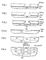
- FIGURES 1-6 are schematic cross-sectional elevation views showing the essence of the steps of forming a device in accordance with the present invention.
- this invention achieves a substrate contact at the top surface of the integrated circuit chip requiring only a single masking operation.
- the processing method begins with a silicon substrate 2 of one conductivity type.
- the embodiment shown in Figure 1 utilizes a P-substrate having formed thereon a thin silicon dioxide layer 3.
- an N-type layer 4 is formed beneath the oxide layer 3.
- a layer of photoresist 8 is coated having a thickness of approximately 1.5 microns. Utilizing a technique such as described in U.S. Patent 4,104,070, patterns are deliberately formed in the photoresist 8 having inverse mesa-like cross-sections as shown in Figure 1.
- the vertical walls in the patterned photoresist 8 taper inward from its top surface at an angle of approximately 45°-55° to form the edge slopes as illustrated.
- a selective etchant is used to etch the exposed portions of oxide 3. Either a gas or liquid etchant such as buffered hydrofluoric acid which does not attack the photoresist may be used. A selective etchant is used next to etch the newly exposed portions of silicon. Once again either a gas or liquid etchant such as pyrocatechol which selectively etches only silicon may be used. In this etching, the exposed silicon is etched to a depth slightly greater than that of the depth of the N implant layer 4. A typical etching depth is in ° the range of 2000 A. As a result, the structure shown in Figure 2 results.
- a thin layer of Si x N y is deposited over the wafer surface.
- This layer 10 is .deposited at a low temperature, such as approximately 245°C over the wafer surface.
- a P-type impurity 12 is deposited beneath the Si x N y layer as illustrated in Figure 3.
- the Si x N y layer is not necessary but preferred to serve as a screen layer during implantation of the P impurity 12.
- the inverse mesa-like structure of the photoresist serves as a mask during the P implant to situate the P implant approximately 1.2-1.5 ⁇ m away from the bottom peripheral portion of the inverse mesa. This typical distance, 1.2-1.5 ⁇ m is shown in Figure 3 as the distance "a".
- the distance "a” is determined by the thickness and the edge slope of the photoresist layer 8.
- Figure 4 illustrates the removal of the Si x N y layer 10 utilizing, for example, hot H 3 P0 4 acid. Then, the photoresist 8 is stripped off leaving the structure as illustrated in Figure 4. By heating, the N and P impurities are driven into the structure to obtain the device shown in Figure 5.
- the next step is the removal of the Si0 2 layer 3 and then forming an N- epi layer 14 in the structure. This is followed by formation of a N reach-through, P base and N emitter in a conventional fashion. Windows for metal contacts are opened in the conventional passivation layers at the top surface of the substrate. Deep dielectric isolation walls 18 are formed at a suitable stage in the above processing in accordance with known prior art techniques. The device fabrication is completed by obtaining interconnection metallization patterns following a conventional method.
- Figure 6 therefore illustrates the essential wafer cross-section of the substrate contacting region.
- the P region 16 is that region which is formed simultaneously with the P base and merges with the upward diffused P region 12 to provide a P substrate reach-through.
- the P region 22 in Figure 6 represents a channel stopper which may have been formed beneath the deep dielectric isolation regions 18 in accordance with the prior art. During processing, P regions 12 and 22 preferably merge to minimize substrate reach-through resistance.
- Figure 6 also illustrates the presence of a Si0 2 -Si 3 N 9 passivation layer which may have been formed on the top surface of the substrate. This is illustrated as layer 20 in Figure 6.
- the step of etching the silicon as shown in Figure 2 simultaneously serves two distinct and independent purposes. First, it removes the N implantation layer in the desired regions. Secondly, it provides a topographical step which aids later mask alignments.
- N 4 and P 12 doped regions are rather heavily doped for well-known reasons, the above processing method specifically prevents their merger at high concentration levels. It is known that if these heavily doped regions are allowed to merge, i.e., form a junction, at relatively high concentration levels, then that often leads to the formation of silicon defects during subsequent conventional processing.
- the present invention prevents merger of the rather heavily doped N 4 and P 12 regions at high concentration levels, first, by the deliberate realization of inverse mesa shapes in the photoresist 8 and, second, by exploiting the fact that photoresist can serve as a mask against ion implantation into silicon directly beneath it.
- the N 4 and P 12 regions are thus separated by distance "a" at the time of introduction of the P 12 dopant. At the end of all hot processing, it is therefore ensured that the junction of N 4 and P 12 regions is at very moderate or low concentration levels.
Applications Claiming Priority (2)
| Application Number | Priority Date | Filing Date | Title |
|---|---|---|---|
| US06/561,507 US4584763A (en) | 1983-12-15 | 1983-12-15 | One mask technique for substrate contacting in integrated circuits involving deep dielectric isolation |
| US561507 | 1983-12-15 |
Publications (3)
| Publication Number | Publication Date |
|---|---|
| EP0146760A2 true EP0146760A2 (de) | 1985-07-03 |
| EP0146760A3 EP0146760A3 (en) | 1989-03-08 |
| EP0146760B1 EP0146760B1 (de) | 1991-07-24 |
Family
ID=24242263
Family Applications (1)
| Application Number | Title | Priority Date | Filing Date |
|---|---|---|---|
| EP84113732A Expired EP0146760B1 (de) | 1983-12-15 | 1984-11-14 | Verfahren zur Herstellung eines Substratkontakts für integrierte Schaltung mittels eines Markierungsschritts |
Country Status (4)
| Country | Link |
|---|---|
| US (1) | US4584763A (de) |
| EP (1) | EP0146760B1 (de) |
| JP (1) | JPS60130134A (de) |
| DE (1) | DE3484846D1 (de) |
Cited By (1)
| Publication number | Priority date | Publication date | Assignee | Title |
|---|---|---|---|---|
| EP0216435A2 (de) * | 1985-09-25 | 1987-04-01 | Advanced Micro Devices, Inc. | Bipolare integrierte Schaltung mit Isolationsstruktur und Substratkontakt und Verfahren zur Herstellung |
Families Citing this family (4)
| Publication number | Priority date | Publication date | Assignee | Title |
|---|---|---|---|---|
| FR2562326B1 (fr) * | 1984-03-30 | 1987-01-23 | Bois Daniel | Procede de fabrication de zones d'isolation electrique des composants d'un circuit integre |
| US4700462A (en) * | 1986-10-08 | 1987-10-20 | Hughes Aircraft Company | Process for making a T-gated transistor |
| US4871689A (en) * | 1987-11-17 | 1989-10-03 | Motorola Inc. | Multilayer trench isolation process and structure |
| WO1993016494A1 (en) * | 1992-01-31 | 1993-08-19 | Analog Devices, Inc. | Complementary bipolar polysilicon emitter devices |
Citations (4)
| Publication number | Priority date | Publication date | Assignee | Title |
|---|---|---|---|---|
| US3909304A (en) * | 1974-05-03 | 1975-09-30 | Western Electric Co | Method of doping a semiconductor body |
| US4044452A (en) * | 1976-10-06 | 1977-08-30 | International Business Machines Corporation | Process for making field effect and bipolar transistors on the same semiconductor chip |
| US4261763A (en) * | 1979-10-01 | 1981-04-14 | Burroughs Corporation | Fabrication of integrated circuits employing only ion implantation for all dopant layers |
| EP0071665A1 (de) * | 1981-08-08 | 1983-02-16 | Deutsche ITT Industries GmbH | Verfahren zum Herstellen einer monolithisch integrierten Festkörperschaltung mit mindestens einem bipolaren Planartransistor |
Family Cites Families (9)
| Publication number | Priority date | Publication date | Assignee | Title |
|---|---|---|---|---|
| US3817750A (en) * | 1970-05-05 | 1974-06-18 | Licentia Gmbh | Method of producing a semiconductor device |
| DE2529054C2 (de) * | 1975-06-30 | 1982-04-29 | Ibm Deutschland Gmbh, 7000 Stuttgart | Verfahren zur Herstellung eines zur Vorlage negativen Resistbildes |
| GB1545208A (en) * | 1975-09-27 | 1979-05-02 | Plessey Co Ltd | Electrical solid state devices |
| US4196228A (en) * | 1978-06-10 | 1980-04-01 | Monolithic Memories, Inc. | Fabrication of high resistivity semiconductor resistors by ion implanatation |
| US4256514A (en) * | 1978-11-03 | 1981-03-17 | International Business Machines Corporation | Method for forming a narrow dimensioned region on a body |
| US4309812A (en) * | 1980-03-03 | 1982-01-12 | International Business Machines Corporation | Process for fabricating improved bipolar transistor utilizing selective etching |
| US4472873A (en) * | 1981-10-22 | 1984-09-25 | Fairchild Camera And Instrument Corporation | Method for forming submicron bipolar transistors without epitaxial growth and the resulting structure |
| JPS59920A (ja) * | 1982-06-23 | 1984-01-06 | Fujitsu Ltd | 半導体装置の製造方法 |
| US4498224A (en) * | 1982-12-23 | 1985-02-12 | Tokyo Shibaura Denki Kabushiki Kaisha | Method of manufacturing a MOSFET using accelerated ions to form an amorphous region |
-
1983
- 1983-12-15 US US06/561,507 patent/US4584763A/en not_active Expired - Fee Related
-
1984
- 1984-08-20 JP JP59171658A patent/JPS60130134A/ja active Granted
- 1984-11-14 EP EP84113732A patent/EP0146760B1/de not_active Expired
- 1984-11-14 DE DE8484113732T patent/DE3484846D1/de not_active Expired - Fee Related
Patent Citations (4)
| Publication number | Priority date | Publication date | Assignee | Title |
|---|---|---|---|---|
| US3909304A (en) * | 1974-05-03 | 1975-09-30 | Western Electric Co | Method of doping a semiconductor body |
| US4044452A (en) * | 1976-10-06 | 1977-08-30 | International Business Machines Corporation | Process for making field effect and bipolar transistors on the same semiconductor chip |
| US4261763A (en) * | 1979-10-01 | 1981-04-14 | Burroughs Corporation | Fabrication of integrated circuits employing only ion implantation for all dopant layers |
| EP0071665A1 (de) * | 1981-08-08 | 1983-02-16 | Deutsche ITT Industries GmbH | Verfahren zum Herstellen einer monolithisch integrierten Festkörperschaltung mit mindestens einem bipolaren Planartransistor |
Non-Patent Citations (3)
| Title |
|---|
| IBM TECHNICAL DISCLOSURE BULLETIN, vol. 21, no. 10, March 1979, page 4081, New York, US; M. BRISKA et al.: "Subisolation diffusion into selected areas adjoining highly n+ doped areas without the use of an oxide mask" * |
| IBM TECHNICAL DISCLOSURE BULLETIN, vol. 23, no. 1, June 1980, page 170, New York, US; B.M. KEMLAGE et al.: "Fabrication of substrate contacts" * |
| IBM TECHNICAL DISCLOSURE BULLETIN, vol. 23, no. 6, November 1980, pages 2243-2244, New York, US; E. ADLER: "Recessed oxide isolation with self-aligned field implant" * |
Cited By (2)
| Publication number | Priority date | Publication date | Assignee | Title |
|---|---|---|---|---|
| EP0216435A2 (de) * | 1985-09-25 | 1987-04-01 | Advanced Micro Devices, Inc. | Bipolare integrierte Schaltung mit Isolationsstruktur und Substratkontakt und Verfahren zur Herstellung |
| EP0216435A3 (en) * | 1985-09-25 | 1990-07-04 | Advanced Micro Devices, Inc. | Bipolar integrated circuit having an improved isolation and substrate connection, and method of preparing the same |
Also Published As
| Publication number | Publication date |
|---|---|
| EP0146760A3 (en) | 1989-03-08 |
| JPS60130134A (ja) | 1985-07-11 |
| JPS645463B2 (de) | 1989-01-30 |
| DE3484846D1 (de) | 1991-08-29 |
| US4584763A (en) | 1986-04-29 |
| EP0146760B1 (de) | 1991-07-24 |
Similar Documents
| Publication | Publication Date | Title |
|---|---|---|
| US5279978A (en) | Process for making BiCMOS device having an SOI substrate | |
| US5166767A (en) | Sidewall contact bipolar transistor with controlled lateral spread of selectively grown epitaxial layer | |
| EP0061729B1 (de) | Verfahren zur Herstellung von Strukturen mit integrierten Halbleiterkomponenten mit Mesa-Konfiguration und Struktur diesen Typs | |
| CA1120609A (en) | Method for forming a narrow dimensioned mask opening on a silicon body | |
| EP0139165B1 (de) | Verfahren zur Herstellung einer integrierten Schaltungsanordnung mit Isolierwannen | |
| EP0036082A1 (de) | Selbstjustierendes Verfahren zur Herstellung eines verbesserten hochqualitativen Bipolartransistors | |
| EP0036111A2 (de) | Verfahren zur Herstellung einer feinen, tiefen dielektrischen Isolation | |
| EP0083816B1 (de) | Halbleiteranordnung mit einem Verbindungsmuster | |
| US4641416A (en) | Method of making an integrated circuit structure with self-aligned oxidation to isolate extrinsic base from emitter | |
| US5434092A (en) | Method for fabricating a triple self-aligned bipolar junction transistor | |
| US4824797A (en) | Self-aligned channel stop | |
| US4887144A (en) | Topside substrate contact in a trenched semiconductor structure and method of fabrication | |
| US4997775A (en) | Method for forming a complementary bipolar transistor structure including a self-aligned vertical PNP transistor | |
| US4853342A (en) | Method of manufacturing semiconductor integrated circuit device having transistor | |
| EP0193116A2 (de) | Verfahren zum Herstellen eines Halbleiterbauelements mit einem Graben | |
| EP0421507B1 (de) | Verfahren zur Herstellung eines bipolaren Transistors | |
| US5144403A (en) | Bipolar transistor with trench-isolated emitter | |
| EP0146760B1 (de) | Verfahren zur Herstellung eines Substratkontakts für integrierte Schaltung mittels eines Markierungsschritts | |
| JPH0254934A (ja) | バイポーラトランジスタの製造方法 | |
| US5147809A (en) | Method of producing a bipolar transistor with a laterally graded emitter (LGE) employing a refill method of polycrystalline silicon | |
| US6617646B2 (en) | Reduced substrate capacitance high performance SOI process | |
| EP0066280A2 (de) | Verfahren zur Herstellung einer Halbleitervorrichtung | |
| US5571731A (en) | Procedure for the manufacture of bipolar transistors without epitaxy and with fully implanted base and collector regions which are self-positioning relative to each other | |
| US3998674A (en) | Method for forming recessed regions of thermally oxidized silicon and structures thereof utilizing anisotropic etching | |
| US5747374A (en) | Methods of fabricating bipolar transistors having separately formed intrinsic base and link-up regions |
Legal Events
| Date | Code | Title | Description |
|---|---|---|---|
| PUAI | Public reference made under article 153(3) epc to a published international application that has entered the european phase |
Free format text: ORIGINAL CODE: 0009012 |
|
| 17P | Request for examination filed |
Effective date: 19841214 |
|
| AK | Designated contracting states |
Designated state(s): DE FR GB |
|
| PUAL | Search report despatched |
Free format text: ORIGINAL CODE: 0009013 |
|
| AK | Designated contracting states |
Kind code of ref document: A3 Designated state(s): DE FR GB |
|
| 17Q | First examination report despatched |
Effective date: 19901002 |
|
| GRAA | (expected) grant |
Free format text: ORIGINAL CODE: 0009210 |
|
| AK | Designated contracting states |
Kind code of ref document: B1 Designated state(s): DE FR GB |
|
| REF | Corresponds to: |
Ref document number: 3484846 Country of ref document: DE Date of ref document: 19910829 |
|
| ET | Fr: translation filed | ||
| PLBE | No opposition filed within time limit |
Free format text: ORIGINAL CODE: 0009261 |
|
| STAA | Information on the status of an ep patent application or granted ep patent |
Free format text: STATUS: NO OPPOSITION FILED WITHIN TIME LIMIT |
|
| 26N | No opposition filed | ||
| PGFP | Annual fee paid to national office [announced via postgrant information from national office to epo] |
Ref country code: GB Payment date: 19951024 Year of fee payment: 12 |
|
| PGFP | Annual fee paid to national office [announced via postgrant information from national office to epo] |
Ref country code: FR Payment date: 19951107 Year of fee payment: 12 |
|
| PGFP | Annual fee paid to national office [announced via postgrant information from national office to epo] |
Ref country code: DE Payment date: 19951123 Year of fee payment: 12 |
|
| PG25 | Lapsed in a contracting state [announced via postgrant information from national office to epo] |
Ref country code: GB Effective date: 19961114 |
|
| GBPC | Gb: european patent ceased through non-payment of renewal fee |
Effective date: 19961114 |
|
| PG25 | Lapsed in a contracting state [announced via postgrant information from national office to epo] |
Ref country code: FR Effective date: 19970731 |
|
| PG25 | Lapsed in a contracting state [announced via postgrant information from national office to epo] |
Ref country code: DE Effective date: 19970801 |
|
| REG | Reference to a national code |
Ref country code: FR Ref legal event code: ST |