EP0146002A2 - Vorrichtung zur Herstellung eines Einkristalls und Steuerung der Herstellung - Google Patents
Vorrichtung zur Herstellung eines Einkristalls und Steuerung der Herstellung Download PDFInfo
- Publication number
- EP0146002A2 EP0146002A2 EP84114131A EP84114131A EP0146002A2 EP 0146002 A2 EP0146002 A2 EP 0146002A2 EP 84114131 A EP84114131 A EP 84114131A EP 84114131 A EP84114131 A EP 84114131A EP 0146002 A2 EP0146002 A2 EP 0146002A2
- Authority
- EP
- European Patent Office
- Prior art keywords
- single crystal
- container
- ray
- hot zone
- shaft
- Prior art date
- Legal status (The legal status is an assumption and is not a legal conclusion. Google has not performed a legal analysis and makes no representation as to the accuracy of the status listed.)
- Granted
Links
- 239000013078 crystal Substances 0.000 title claims abstract description 55
- 238000004519 manufacturing process Methods 0.000 title claims description 7
- 238000012544 monitoring process Methods 0.000 title description 4
- 239000000463 material Substances 0.000 claims abstract description 16
- 238000000034 method Methods 0.000 claims abstract description 12
- 238000002594 fluoroscopy Methods 0.000 claims abstract description 8
- 239000003566 sealing material Substances 0.000 claims abstract description 8
- 238000002834 transmittance Methods 0.000 claims abstract description 6
- 238000010521 absorption reaction Methods 0.000 claims abstract description 5
- 238000010438 heat treatment Methods 0.000 claims abstract description 5
- 230000000737 periodic effect Effects 0.000 claims abstract description 5
- PZNSFCLAULLKQX-UHFFFAOYSA-N Boron nitride Chemical compound N#B PZNSFCLAULLKQX-UHFFFAOYSA-N 0.000 claims description 6
- OKTJSMMVPCPJKN-UHFFFAOYSA-N Carbon Chemical compound [C] OKTJSMMVPCPJKN-UHFFFAOYSA-N 0.000 claims description 4
- 239000007788 liquid Substances 0.000 claims description 4
- 239000010453 quartz Substances 0.000 claims description 4
- VYPSYNLAJGMNEJ-UHFFFAOYSA-N silicon dioxide Inorganic materials O=[Si]=O VYPSYNLAJGMNEJ-UHFFFAOYSA-N 0.000 claims description 4
- 229910052582 BN Inorganic materials 0.000 claims description 3
- PMHQVHHXPFUNSP-UHFFFAOYSA-M copper(1+);methylsulfanylmethane;bromide Chemical compound Br[Cu].CSC PMHQVHHXPFUNSP-UHFFFAOYSA-M 0.000 claims description 3
- 229910002804 graphite Inorganic materials 0.000 claims description 3
- 239000010439 graphite Substances 0.000 claims description 3
- 239000002994 raw material Substances 0.000 description 7
- 229910001218 Gallium arsenide Inorganic materials 0.000 description 6
- 239000000203 mixture Substances 0.000 description 5
- 239000012535 impurity Substances 0.000 description 3
- 229910052799 carbon Inorganic materials 0.000 description 2
- 150000001875 compounds Chemical class 0.000 description 2
- 238000010276 construction Methods 0.000 description 2
- 239000012611 container material Substances 0.000 description 2
- 238000007796 conventional method Methods 0.000 description 2
- 238000001004 secondary ion mass spectrometry Methods 0.000 description 2
- 229910005540 GaP Inorganic materials 0.000 description 1
- 229910000673 Indium arsenide Inorganic materials 0.000 description 1
- 239000013543 active substance Substances 0.000 description 1
- 229910052782 aluminium Inorganic materials 0.000 description 1
- 230000007547 defect Effects 0.000 description 1
- 238000001514 detection method Methods 0.000 description 1
- 230000000694 effects Effects 0.000 description 1
- RPQDHPTXJYYUPQ-UHFFFAOYSA-N indium arsenide Chemical compound [In]#[As] RPQDHPTXJYYUPQ-UHFFFAOYSA-N 0.000 description 1
- 238000005259 measurement Methods 0.000 description 1
- 238000012986 modification Methods 0.000 description 1
- 230000004048 modification Effects 0.000 description 1
- 238000007789 sealing Methods 0.000 description 1
- 230000035945 sensitivity Effects 0.000 description 1
- 239000007787 solid Substances 0.000 description 1
- 229910001220 stainless steel Inorganic materials 0.000 description 1
- 239000010935 stainless steel Substances 0.000 description 1
- 239000000758 substrate Substances 0.000 description 1
- 230000008016 vaporization Effects 0.000 description 1
- 238000009736 wetting Methods 0.000 description 1
Images
Classifications
-
- C—CHEMISTRY; METALLURGY
- C30—CRYSTAL GROWTH
- C30B—SINGLE-CRYSTAL GROWTH; UNIDIRECTIONAL SOLIDIFICATION OF EUTECTIC MATERIAL OR UNIDIRECTIONAL DEMIXING OF EUTECTOID MATERIAL; REFINING BY ZONE-MELTING OF MATERIAL; PRODUCTION OF A HOMOGENEOUS POLYCRYSTALLINE MATERIAL WITH DEFINED STRUCTURE; SINGLE CRYSTALS OR HOMOGENEOUS POLYCRYSTALLINE MATERIAL WITH DEFINED STRUCTURE; AFTER-TREATMENT OF SINGLE CRYSTALS OR A HOMOGENEOUS POLYCRYSTALLINE MATERIAL WITH DEFINED STRUCTURE; APPARATUS THEREFOR
- C30B15/00—Single-crystal growth by pulling from a melt, e.g. Czochralski method
- C30B15/10—Crucibles or containers for supporting the melt
-
- C—CHEMISTRY; METALLURGY
- C30—CRYSTAL GROWTH
- C30B—SINGLE-CRYSTAL GROWTH; UNIDIRECTIONAL SOLIDIFICATION OF EUTECTIC MATERIAL OR UNIDIRECTIONAL DEMIXING OF EUTECTOID MATERIAL; REFINING BY ZONE-MELTING OF MATERIAL; PRODUCTION OF A HOMOGENEOUS POLYCRYSTALLINE MATERIAL WITH DEFINED STRUCTURE; SINGLE CRYSTALS OR HOMOGENEOUS POLYCRYSTALLINE MATERIAL WITH DEFINED STRUCTURE; AFTER-TREATMENT OF SINGLE CRYSTALS OR A HOMOGENEOUS POLYCRYSTALLINE MATERIAL WITH DEFINED STRUCTURE; APPARATUS THEREFOR
- C30B15/00—Single-crystal growth by pulling from a melt, e.g. Czochralski method
- C30B15/20—Controlling or regulating
- C30B15/22—Stabilisation or shape controlling of the molten zone near the pulled crystal; Controlling the section of the crystal
- C30B15/26—Stabilisation or shape controlling of the molten zone near the pulled crystal; Controlling the section of the crystal using television detectors; using photo or X-ray detectors
-
- Y—GENERAL TAGGING OF NEW TECHNOLOGICAL DEVELOPMENTS; GENERAL TAGGING OF CROSS-SECTIONAL TECHNOLOGIES SPANNING OVER SEVERAL SECTIONS OF THE IPC; TECHNICAL SUBJECTS COVERED BY FORMER USPC CROSS-REFERENCE ART COLLECTIONS [XRACs] AND DIGESTS
- Y10—TECHNICAL SUBJECTS COVERED BY FORMER USPC
- Y10S—TECHNICAL SUBJECTS COVERED BY FORMER USPC CROSS-REFERENCE ART COLLECTIONS [XRACs] AND DIGESTS
- Y10S117/00—Single-crystal, oriented-crystal, and epitaxy growth processes; non-coating apparatus therefor
- Y10S117/90—Apparatus characterized by composition or treatment thereof, e.g. surface finish, surface coating
-
- Y—GENERAL TAGGING OF NEW TECHNOLOGICAL DEVELOPMENTS; GENERAL TAGGING OF CROSS-SECTIONAL TECHNOLOGIES SPANNING OVER SEVERAL SECTIONS OF THE IPC; TECHNICAL SUBJECTS COVERED BY FORMER USPC CROSS-REFERENCE ART COLLECTIONS [XRACs] AND DIGESTS
- Y10—TECHNICAL SUBJECTS COVERED BY FORMER USPC
- Y10T—TECHNICAL SUBJECTS COVERED BY FORMER US CLASSIFICATION
- Y10T117/00—Single-crystal, oriented-crystal, and epitaxy growth processes; non-coating apparatus therefor
- Y10T117/10—Apparatus
- Y10T117/1004—Apparatus with means for measuring, testing, or sensing
- Y10T117/1012—Apparatus with means for measuring, testing, or sensing with a window or port for visual observation or examination
-
- Y—GENERAL TAGGING OF NEW TECHNOLOGICAL DEVELOPMENTS; GENERAL TAGGING OF CROSS-SECTIONAL TECHNOLOGIES SPANNING OVER SEVERAL SECTIONS OF THE IPC; TECHNICAL SUBJECTS COVERED BY FORMER USPC CROSS-REFERENCE ART COLLECTIONS [XRACs] AND DIGESTS
- Y10—TECHNICAL SUBJECTS COVERED BY FORMER USPC
- Y10T—TECHNICAL SUBJECTS COVERED BY FORMER US CLASSIFICATION
- Y10T117/00—Single-crystal, oriented-crystal, and epitaxy growth processes; non-coating apparatus therefor
- Y10T117/10—Apparatus
- Y10T117/1024—Apparatus for crystallization from liquid or supercritical state
- Y10T117/1032—Seed pulling
- Y10T117/106—Seed pulling including sealing means details
-
- Y—GENERAL TAGGING OF NEW TECHNOLOGICAL DEVELOPMENTS; GENERAL TAGGING OF CROSS-SECTIONAL TECHNOLOGIES SPANNING OVER SEVERAL SECTIONS OF THE IPC; TECHNICAL SUBJECTS COVERED BY FORMER USPC CROSS-REFERENCE ART COLLECTIONS [XRACs] AND DIGESTS
- Y10—TECHNICAL SUBJECTS COVERED BY FORMER USPC
- Y10T—TECHNICAL SUBJECTS COVERED BY FORMER US CLASSIFICATION
- Y10T117/00—Single-crystal, oriented-crystal, and epitaxy growth processes; non-coating apparatus therefor
- Y10T117/10—Apparatus
- Y10T117/1024—Apparatus for crystallization from liquid or supercritical state
- Y10T117/1032—Seed pulling
- Y10T117/1064—Seed pulling including a fully-sealed or vacuum-maintained crystallization chamber [e.g., ampoule]
Definitions
- the present invention relates to an apparatus for production of a single crystal and to monitoring the production. It is applicable to an apparatus for producing a single crystal of a compound consisting of elements of the III-V groups of the periodic table having high vapor pressure (hereinafter referred to as "volatile elements”) by a Czochralski method (hereinafter referred to as "CZ method").
- a hot wall method in which a liquid sealing material such as molten B 2 0 3 is used as a sealing material for sealing the apparatus.
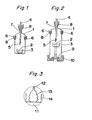
- a single crystal is pulled up in a container 1 having a structure shown in Fig. 1 which is filled with vapor of volatile component elements of the single crystal (eg. As).
- the container 1 is provided with a crucible 3 containing a molten raw material 2 and a pulling shaft 4 which pulls up the single crystal with rotation.
- a seed crystal 5 is attached to the lower end of the shaft 4.
- the container is divided into upper and lower portions at a certain part of a side wall, and liquid sealing materials 8 seal an opening 6 of the container and a gap 7 between the pulling shaft 4 and the container 1.
- the seed crystal is dipped in a surface of the molten raw material in the crucible 3 and, after wetting, pulls up the single crystal with rotation of the seed crystal 5.
- the container 1 used in this method is made of quartz, in case of the production of, for example, a GaAs single crystal, the raw material reacts with quarts as follows: and GaAs is contaminated with Si. Therefore, it is difficult to produce, for example, a single crystal suitable for the production of an undoped semi-insulating substrate by the above conventional method.
- PBN pyrolytic boron nitride
- the vapor of the component elements filling the container is supplied by vaporizing solid elements which are beforehand charged in the container in excess amounts, and the vapor pressure is not controlled during pulling up the single crystal. Therefore, a composition of the single crystal cannot be controlled, so that it is difficult to produce a high quality single crystal containing less impurities and having less inherent and crystal defects.
- One object of the invention is to provide an apparatus for producing a single crystal which is not contaminated with an electrically active substances immigrated from a container material of the apparatus.
- Another object of the invention is to provide an apparatus for producing a single crystal by which vapor pressure of volatile component elements is controlled so as to adjust a composition of a molten raw material.
- Further object of the invention is to provide an apparatus for producing a single crystal by which growth of the pulled single crystal can be monitored by X-ray fluoroscopy.
- an apparatus for producing a single crystal according to the CZ method which comprises
- Examples of the single crystal to be produced by means of the apparatus of the invention are those made of compounds of volatile component elements such as those of the III-V groups of the periodic table (eg. GaAs, GaP, InAs, InP, etc.).
- Fig. 2 shows an embodiment of the apparatus of the invention.
- Fig 2 shows an embodiment of the apparatus of the invention.
- the same numerals indicate the same or corresponding parts in Fig. 1.
- the illustrated apparatus of the invention has generally a similar construction to that of Fig. 1 which is used in the hot wall method. However, the apparatus of the invention may have a different construction.
- the container 1 there are positioned reservoirs 9 for supplying the volatile component elements such as As.
- a temperature of the portion of the container where the reservoirs are positioned is controlled by a reservoir heating means 10 independently from the temperature of the portion where the single crystal is pulled up, thereby controlling the vapor pressure of the component elements in the container 1 to prevent fluctuation of the composition of the molten raw material from the stoichiometric composition.
- At least a part of the container 1 which contacts the vapor of the component elements is made of a material which is isoelectronic with one of the component elements of the single crystal.
- a material which is isoelectronic with one of the component elements of the single crystal examples include boron nitride (hereinafter referred to as "BN”), PBN and aluminum nitride (hereinafter referred to as "A1N").
- Said part of the container may be made of the material itself, or of graphite or quartz coated with the material. Thereby, the molten raw material is not contaminated with electrically active impurities contained in the container material.
- Quality and thickness of the whole hot zone including the container 1, an outer chamber, a susceptor, crucible 3, etc are selected so that the X-ray mass absorption coefficient of the hot zone is not larger than 5 cm 2 /g.
- the hot zone is made so as to have such thickness that the hot zone is made so that X-ray transmittance through the whole hot zone is 10 -6 or more so as to monitor the single crystal being pulled up in the opaque container by X-ray fluoroscopy.
- the X-ray mass absorption coefficient is larger than 5 cm 2 /g, it is difficult to see the shape of the single crystal by X-ray fluoroscopy.
- the X-ray transmittance is less than 10- 6 , contrast of the fluoroscopic image is deteriorated and sufficient detection sensitivity of the X-ray detector is not achieved.
- X-ray fluoroscopy is carried out by radiating near the crucible by means of an X-ray generator and detecting X-ray transmitted through the apparatus by an X-ray detector.
- the apparatus had an outer chamber having an outer diameter of 280 mm made of stainless steel (SUS 304) having a thickness of 4 mm, and the container 1 made of BN-coated graphite having an outer diameter of 150 mm and a wall thickness of 6 mm in the outer chamber.
- the liquid sealing material 8 molten B 2 0 3 was used.
- the crucible 3 was made of PBN and the means for heating the crucible was a carbon heater having a thickness of 8 mm.
- GaAs having a stoichiometric composition was charged and heated at 1,238°C.
- the single crystal in the apparatus was monitored by a fluoroscopic apparatus (Voltage of X-ray tube 105 kV, 2 mA) through a monitoring image as shown in Fig. 3, which shows the molten raw material 11, the seed crystal 12, the single crystal 13 and the crucible wall 14 made of PBN.
- the total X-ray transmittance of the apparatus was 1.2 x 10 6.
- the shaft 4 was pulled up at a pulling rate of 6 mm/min. with a rotation rate of 2 rpm to obtain 1.1 kg of the single crystal of about 2" in diameter and 90 mm in length.
- the thus produced single crystal was analyzed by SIMS (Secondary Ion Mass Spectroscopy) to find that the number of each the impurities (eg. Si, C, 0, Al, Mg, Ca, Cr, Fe, etc.) was less than 1 x 10 cm , and had good semi-insulating property having specific resistivity of about 10 8 ohm.cm.
- impurities eg. Si, C, 0, Al, Mg, Ca, Cr, Fe, etc.
- EPD etch pit density
- Hall mobility of the single crystal was as high as 4,500 cm 2 /V.sec.
- a single crystal of GaAs produced by the conventional method was a conductive one containing about 6 x 10 16 cm -3 of S i and having specific resistivity of about 10 2 ohm.cm.
Landscapes
- Chemical & Material Sciences (AREA)
- Engineering & Computer Science (AREA)
- Crystallography & Structural Chemistry (AREA)
- Materials Engineering (AREA)
- Metallurgy (AREA)
- Organic Chemistry (AREA)
- Crystals, And After-Treatments Of Crystals (AREA)
- Liquid Deposition Of Substances Of Which Semiconductor Devices Are Composed (AREA)
Applications Claiming Priority (2)
| Application Number | Priority Date | Filing Date | Title |
|---|---|---|---|
| JP219744/83 | 1983-11-22 | ||
| JP58219744A JPS60112695A (ja) | 1983-11-22 | 1983-11-22 | 化合物単結晶の引上方法 |
Publications (3)
| Publication Number | Publication Date |
|---|---|
| EP0146002A2 true EP0146002A2 (de) | 1985-06-26 |
| EP0146002A3 EP0146002A3 (en) | 1985-12-27 |
| EP0146002B1 EP0146002B1 (de) | 1988-06-15 |
Family
ID=16740305
Family Applications (1)
| Application Number | Title | Priority Date | Filing Date |
|---|---|---|---|
| EP84114131A Expired EP0146002B1 (de) | 1983-11-22 | 1984-11-22 | Vorrichtung zur Herstellung eines Einkristalls und Steuerung der Herstellung |
Country Status (5)
| Country | Link |
|---|---|
| US (1) | US4596700A (de) |
| EP (1) | EP0146002B1 (de) |
| JP (1) | JPS60112695A (de) |
| CA (1) | CA1238839A (de) |
| DE (1) | DE3472117D1 (de) |
Cited By (2)
| Publication number | Priority date | Publication date | Assignee | Title |
|---|---|---|---|---|
| EP0166500A1 (de) * | 1984-04-23 | 1986-01-02 | Kabushiki Kaisha Toshiba | Vorrichtung zur Herstellung eines Einkristalls aus einer Halbleiterverbindung nach dem Schutzschmelz-Czochralski-Verfahren (LEC) |
| EP0174060A1 (de) * | 1984-06-08 | 1986-03-12 | Sumitomo Electric Industries Limited | Verfahren zur Züchtung von Einkristallen |
Families Citing this family (5)
| Publication number | Priority date | Publication date | Assignee | Title |
|---|---|---|---|---|
| DE68917054T2 (de) * | 1988-08-19 | 1995-01-05 | Mitsubishi Materials Corp | Verfahren zur Einkristallzüchtung von zersetzbaren Halbleiter-Verbindungen. |
| EP0355746B1 (de) * | 1988-08-19 | 1994-07-27 | Mitsubishi Materials Corporation | Verfahren zur Einkristallzüchtung von zersetzbaren Halbleiter-Verbindungen |
| US5158750A (en) * | 1990-06-06 | 1992-10-27 | Praxair S.T. Technology, Inc. | Boron nitride crucible |
| US7604240B2 (en) * | 2002-09-16 | 2009-10-20 | Hewlett-Packard Development Company, L.P. | Capillary seal for a burn chamber |
| JP4565877B2 (ja) * | 2004-04-16 | 2010-10-20 | 日立プラズマディスプレイ株式会社 | プラズマディスプレイ装置 |
Family Cites Families (11)
| Publication number | Priority date | Publication date | Assignee | Title |
|---|---|---|---|---|
| CA729096A (en) * | 1966-03-01 | Radio Corporation Of America | Method of growing crystals | |
| FR1379178A (fr) * | 1962-12-10 | 1964-11-20 | Rca Corp | Procédé de préparation de cristaux |
| NL6512921A (de) * | 1965-10-06 | 1967-04-07 | ||
| FR1568042A (de) * | 1968-01-18 | 1969-05-23 | ||
| NL6917398A (de) * | 1969-03-18 | 1970-09-22 | ||
| US3857679A (en) * | 1973-02-05 | 1974-12-31 | Univ Southern California | Crystal grower |
| JPS508144U (de) * | 1973-05-23 | 1975-01-28 | ||
| JPS57170891A (en) * | 1981-04-15 | 1982-10-21 | Toshiba Corp | Manufacture of single crystal |
| JPS5914440B2 (ja) * | 1981-09-18 | 1984-04-04 | 住友電気工業株式会社 | CaAs単結晶への硼素のド−ピング方法 |
| EP0138292B1 (de) * | 1983-08-06 | 1987-10-14 | Sumitomo Electric Industries Limited | Vorrichtung zur Züchtung von Einkristallen |
| DE3472577D1 (en) * | 1983-08-31 | 1988-08-11 | Japan Res Dev Corp | Apparatus for growing single crystals of dissociative compounds |
-
1983
- 1983-11-22 JP JP58219744A patent/JPS60112695A/ja active Granted
-
1984
- 1984-11-13 US US06/671,080 patent/US4596700A/en not_active Expired - Lifetime
- 1984-11-21 CA CA000468322A patent/CA1238839A/en not_active Expired
- 1984-11-22 EP EP84114131A patent/EP0146002B1/de not_active Expired
- 1984-11-22 DE DE8484114131T patent/DE3472117D1/de not_active Expired
Cited By (3)
| Publication number | Priority date | Publication date | Assignee | Title |
|---|---|---|---|---|
| EP0166500A1 (de) * | 1984-04-23 | 1986-01-02 | Kabushiki Kaisha Toshiba | Vorrichtung zur Herstellung eines Einkristalls aus einer Halbleiterverbindung nach dem Schutzschmelz-Czochralski-Verfahren (LEC) |
| US4668481A (en) * | 1984-04-23 | 1987-05-26 | Kabushiki Kaisha Toshiba | Apparatus for manufacturing a compound-semiconductor single crystal by the liquid encapsulated czochralski (LEC) process |
| EP0174060A1 (de) * | 1984-06-08 | 1986-03-12 | Sumitomo Electric Industries Limited | Verfahren zur Züchtung von Einkristallen |
Also Published As
| Publication number | Publication date |
|---|---|
| EP0146002B1 (de) | 1988-06-15 |
| CA1238839A (en) | 1988-07-05 |
| DE3472117D1 (en) | 1988-07-21 |
| EP0146002A3 (en) | 1985-12-27 |
| JPS60112695A (ja) | 1985-06-19 |
| JPH0567599B2 (de) | 1993-09-27 |
| US4596700A (en) | 1986-06-24 |
Similar Documents
| Publication | Publication Date | Title |
|---|---|---|
| DE69201292T2 (de) | Vorrichtung zur Einkristallziehung. | |
| EP0509312A2 (de) | Czochralsky-Verfahren unter Verwendung eines Bauelementes zum Abschirmen der Strahlung der Rohmaterial-Schmelzlösung und Vorrichtung hierfür | |
| US4134785A (en) | Real-time analysis and control of melt-chemistry in crystal growing operations | |
| US5139750A (en) | Silicon single crystal manufacturing apparatus | |
| EP0139157B1 (de) | Vorrichtung zur Züchtung von einkristallinen zersetzbaren Verbindungen | |
| KR940009938B1 (ko) | 단결정의 인상(引上)방법 | |
| EP0146002B1 (de) | Vorrichtung zur Herstellung eines Einkristalls und Steuerung der Herstellung | |
| Frosch et al. | The preparation and floating zone processing of gallium phosphide | |
| EP0392210B1 (de) | Verfahren zur Züchtung eines Einkristalls | |
| EP0162467B1 (de) | Vorrichtung zur Züchtung von Einkristallen aus zersetzbaren Verbindungen | |
| EP0138292B1 (de) | Vorrichtung zur Züchtung von Einkristallen | |
| US5427056A (en) | Apparatus and method for producing single crystal | |
| US5488923A (en) | Method for producing single crystal | |
| US6984263B2 (en) | Shallow melt apparatus for semicontinuous czochralski crystal growth | |
| EP0210439B1 (de) | Verfahren zur Züchtung von Einkristallen einer zersetzbaren Halbleiterverbindung | |
| EP0166500B1 (de) | Vorrichtung zur Herstellung eines Einkristalls aus einer Halbleiterverbindung nach dem Schutzschmelz-Czochralski-Verfahren (LEC) | |
| EP1498515A1 (de) | Vorrichtung zum ziehen von einkristallen | |
| Cröll et al. | Floating-zone growth of GaAs | |
| EP0355833B1 (de) | Verfahren zur Herstellung eines Einkristalls aus einer Halbleiter-Verbindung | |
| JPH0365593A (ja) | 単結晶成長装置 | |
| JP2719673B2 (ja) | 単結晶成長方法 | |
| Otani et al. | Preparation of LaB6 single crystals by the floating zone method | |
| EP0100453A1 (de) | Verfahren zur Herstellung von einkristallinen GaAs durch Ziehen aus einer GaAs-Schmelze | |
| JP2755452B2 (ja) | シリコン単結晶の引上げ装置 | |
| Müller et al. | Sources of silicon contamination in LEC-grown InP crystals |
Legal Events
| Date | Code | Title | Description |
|---|---|---|---|
| PUAI | Public reference made under article 153(3) epc to a published international application that has entered the european phase |
Free format text: ORIGINAL CODE: 0009012 |
|
| AK | Designated contracting states |
Designated state(s): DE FR GB |
|
| PUAL | Search report despatched |
Free format text: ORIGINAL CODE: 0009013 |
|
| AK | Designated contracting states |
Designated state(s): DE FR GB |
|
| 17P | Request for examination filed |
Effective date: 19860122 |
|
| 17Q | First examination report despatched |
Effective date: 19861204 |
|
| GRAA | (expected) grant |
Free format text: ORIGINAL CODE: 0009210 |
|
| AK | Designated contracting states |
Kind code of ref document: B1 Designated state(s): DE FR GB |
|
| REF | Corresponds to: |
Ref document number: 3472117 Country of ref document: DE Date of ref document: 19880721 |
|
| ET | Fr: translation filed | ||
| PLBE | No opposition filed within time limit |
Free format text: ORIGINAL CODE: 0009261 |
|
| STAA | Information on the status of an ep patent application or granted ep patent |
Free format text: STATUS: NO OPPOSITION FILED WITHIN TIME LIMIT |
|
| 26N | No opposition filed | ||
| PGFP | Annual fee paid to national office [announced via postgrant information from national office to epo] |
Ref country code: FR Payment date: 19991109 Year of fee payment: 16 |
|
| PGFP | Annual fee paid to national office [announced via postgrant information from national office to epo] |
Ref country code: GB Payment date: 19991117 Year of fee payment: 16 |
|
| PGFP | Annual fee paid to national office [announced via postgrant information from national office to epo] |
Ref country code: DE Payment date: 19991119 Year of fee payment: 16 |
|
| PG25 | Lapsed in a contracting state [announced via postgrant information from national office to epo] |
Ref country code: GB Free format text: LAPSE BECAUSE OF NON-PAYMENT OF DUE FEES Effective date: 20001122 |
|
| GBPC | Gb: european patent ceased through non-payment of renewal fee |
Effective date: 20001122 |
|
| PG25 | Lapsed in a contracting state [announced via postgrant information from national office to epo] |
Ref country code: FR Free format text: LAPSE BECAUSE OF NON-PAYMENT OF DUE FEES Effective date: 20010731 |
|
| PG25 | Lapsed in a contracting state [announced via postgrant information from national office to epo] |
Ref country code: DE Free format text: LAPSE BECAUSE OF NON-PAYMENT OF DUE FEES Effective date: 20010801 |
|
| REG | Reference to a national code |
Ref country code: FR Ref legal event code: ST |